EP0949724A2 - Connecteur électrique - Google Patents
Connecteur électrique Download PDFInfo
- Publication number
- EP0949724A2 EP0949724A2 EP99302747A EP99302747A EP0949724A2 EP 0949724 A2 EP0949724 A2 EP 0949724A2 EP 99302747 A EP99302747 A EP 99302747A EP 99302747 A EP99302747 A EP 99302747A EP 0949724 A2 EP0949724 A2 EP 0949724A2
- Authority
- EP
- European Patent Office
- Prior art keywords
- circuit board
- sections
- housing
- electrical connector
- contact
- Prior art date
- Legal status (The legal status is an assumption and is not a legal conclusion. Google has not performed a legal analysis and makes no representation as to the accuracy of the status listed.)
- Withdrawn
Links
Images

Classifications
-
- H—ELECTRICITY
- H01—ELECTRIC ELEMENTS
- H01R—ELECTRICALLY-CONDUCTIVE CONNECTIONS; STRUCTURAL ASSOCIATIONS OF A PLURALITY OF MUTUALLY-INSULATED ELECTRICAL CONNECTING ELEMENTS; COUPLING DEVICES; CURRENT COLLECTORS
- H01R12/00—Structural associations of a plurality of mutually-insulated electrical connecting elements, specially adapted for printed circuits, e.g. printed circuit boards [PCB], flat or ribbon cables, or like generally planar structures, e.g. terminal strips, terminal blocks; Coupling devices specially adapted for printed circuits, flat or ribbon cables, or like generally planar structures; Terminals specially adapted for contact with, or insertion into, printed circuits, flat or ribbon cables, or like generally planar structures
- H01R12/70—Coupling devices
- H01R12/71—Coupling devices for rigid printing circuits or like structures
- H01R12/712—Coupling devices for rigid printing circuits or like structures co-operating with the surface of the printed circuit or with a coupling device exclusively provided on the surface of the printed circuit
- H01R12/714—Coupling devices for rigid printing circuits or like structures co-operating with the surface of the printed circuit or with a coupling device exclusively provided on the surface of the printed circuit with contacts abutting directly the printed circuit; Button contacts therefore provided on the printed circuit
Definitions
- the present invention relates to an electrical connector which has electrical contacts that electrically connect a first circuit board such as card-mounting flexible printed circuits (FPC's) or integrated circuits, or a printed circuit board, and a second circuit board such as a printed circuit board, which is disposed substantially parallel to the first circuit board.
- FPC's card-mounting flexible printed circuits
- a second circuit board such as a printed circuit board
- electrical connector 100 shown in Figures 4A and 4B is known as an electrical card connector, which electrically connects electronic memory cards on which integrated circuits are mounted and printed circuit boards, which are disposed substantially parallel to the electronic memory cards as disclosed in Japanese Patent Application No. 63-155392.
- Electrical card connector 100 is equipped with an insulating housing 110, which has a plurality of openings 111 arranged in two rows, and a plurality of electrical contacts 120, which are fastened to housing 110 in two rows. Electrical contacts 120 electrically connect an electronic memory card (not shown) and a printed circuit board (not shown) that are disposed substantially parallel to each other.
- the respective contacts 120 are formed by stamping and forming a metal plate.
- Each contact 120 is equipped with a fastening section 121 fastened to the housing 110, a cantilever contact section 122, which extends into and across the corresponding opening 111 of the housing 110 from the fastening section 121, and which has an arcuate contact member 123 that electrically engages with a flat surface of a conductive pad on an undersurface of the electronic memory card, and a tine section 124, which extends to the outside of the housing 110 from the fastening section 121 and is electrically connected to the printed circuit board by soldering.
- Posts 112 are provided on housing 110 to position the electrical card connector 100 on the printed circuit board.
- Connector 200 shown in Figures 5A and 5B is known as a surface-mount electrical connector which electrically connects IC chips with printed circuit boards that are disposed substantially parallel to the IC chips as disclosed in Japanese Patent Application No. 6-85342.
- Surface-mount electrical connector 200 is equipped with an insulating housing 210, and a plurality of electrical contacts 220 which are secured to housing 210 in a single row, and which electrically connect an IC chip (not shown) and a printed circuit board (not shown) that are disposed substantially parallel to each other.
- the respective contacts 220 are formed by the stamping of a metal plate.
- Each contact 220 is equipped with a base section 221 which has a press-fitting projection 222 that is press-fit into the housing 210 from beneath, a resilient contact section 223 which extends into the housing 210 from the base section 221, and which has an arcuate contact member 224 that engages with a conductive pad on the undersurface of the IC chip, and a tine section 225 which extends to the outside of the housing 210 from the base section 221, and which is connected to the printed circuit board by soldering.
- a post 211 which is used to position the surface-mount electrical connector 200 on the printed circuit board.
- the contact members 123 of the contact sections 122 of the contacts 120 are arranged so that the contact members 123 engage the conductive pads on the undersurface of the electronic memory card with arcuate surfaces; accordingly, the electrical engagement is smoothly accomplished, and the height of the connector 100 in the vertical direction is lowered.
- the free length of each contact section 122 from the fixed end of the fastening section 121 of the contact 120 with the housing 110 to the contact member 123 is long, and since the contact section 122 flexes in the direction of thickness, sufficient contact pressure may not be achieved when the electronic memory card engages the contact member 123.
- the contact members 224 of the contact sections 223 of the contacts 220 engage the undersurface of the IC chip with a shear surface, and the contact sections 223 flex in the direction perpendicular to the direction of thickness; accordingly, a sufficiently large contact pressure can be obtained when the IC chip engages the contact members 224.
- the width of the stamped arcuate surface of each contact 220 extends in the vertical direction, there are limits to how far the vertical height of the connector 200 can be lowered.
- the object of the present invention is to provide an electrical connector which electrically connects circuit boards that are disposed substantially parallel to each other, and which also makes it possible to lower the height of the connector as a whole, and to increase the contact pressure on the circuit boards.
- the electrical connector of the present invention is equipped with an insulating housing, and electrical contacts which have fastening sections that are fastened to the housing, and which electrically connect a first circuit board and a second circuit board that are disposed substantially parallel to each other, the contacts have cantilever contact sections which extend from the fastening sections, and which resiliently engage an undersurface of the first circuit board with arcuate surfaces stamped and formed from a metal plate, and the cantilever contact sections have supporting-point members which are bent from the fastening sections and engage the surface of the second circuit board, and which act as supporting points when flexed by the first circuit board during engagement therewith.
- the supporting-point members are movable on the second circuit board.
- An electrical connector for interconnecting conductive pads on a first circuit board with conductive pads on a second circuit board comprises a dielectric housing, electrical contacts having fastening sections secured in the housing, tine sections for electrical engagement with the conductive pads on the second circuit board, and cantilever contact sections extending from the fastening sections for electrical engagement with the conductive pads on the first circuit board wherein the cantilever contact sections include supporting-point members for engaging the second circuit board and acting as supporting points when the cantilever contact sections are flexed by engagement with the first circuit board.
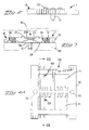
- Figures 1A and 1B show the electrical connector of the present invention
- Figure 1A is a top plan view
- Figure 1B is a front view thereof.
- Figure 2 is a left-side view of the electrical connector shown in Figure 1.
- Figure 3 is a cross-sectional view taken along line 3-3 in Figure 1.
- the first and second circuit boards that are connected to each other by the electrical connector are indicated by broken lines.
- Figures 4A and 4B show a conventional electrical card connector; Figure 4A is a top plan view, and Figure 4B is cross-sectional view taken along line 4B-4B in Figure 4A.
- Figures 5A and 5B show a conventional surface-mount connector; Figure 5A is a top plan view, and Figure 5B is a cross-sectional view taken along line 5B-5B in Figure 5A; however, in Figure 5B, the electrical contacts are not shown in cross-section.
- electrical connector 1 is equipped with an insulating housing 10, and a plurality of electrical contacts 20 which are fastened to housing 10 in two rows, and which electrically connect a first circuit board 30 and second circuit board 40 that are disposed substantially parallel to each other.
- the first circuit board 30 is an FPC (Flexible Printed Circuit)
- the second circuit board 40 is a printed circuit board; however, these circuit boards may also be other types of circuit boards, such as cards mounting integrated circuits thereon.
- the housing 10 is formed substantially into the shape of a rectangular parallelepiped which extends in the direction of length, forming of the housing being accomplished by molding from an insulating resin material.
- Partition walls 10a which delineate the openings 11, are provided in order to insulate the contacts 20 in the direction of the contact row.
- cut-outs 12 which are used to ascertain visually or by means of an automatic inspection device whether or not tine sections 25 of the plurality of contacts 20 (described later) are properly soldered to the conductive pads of the second circuit board 40, are located in both side walls of the housing 10 with respect to the direction perpendicular to the direction of length.
- each contact 20 of the respective rows is arranged at a uniform pitch along the direction of length of the housing 10, and pairs of mutually facing contacts 20 of different rows are disposed inside the respective openings 11 of the housing 10.
- the respective electrical contacts 20 are formed by stamping and forming a metal plate; each contact is equipped with a fastening section 21, which is fastened to the housing 10 by insert molding, a cantilever contact section 22, which extends into the opening 11 of the housing 10 from the fastening section 21, and a tine section 25, which extends to the outside of the housing 10 from the fastening section 21 and which is fastened by soldering to a conductive pad on the second circuit board 40.
- the cantilever contact section 22 has a supporting-point member 24, which is bent from the fastening section 21 and engages a surface of the second circuit board 40 and which acts as a supporting point when the cantilever contact section is flexed by the first circuit board 30. Furthermore, the cantilever contact section 22 extends upward at an inclination toward the inside of the corresponding opening 11 from the supporting-point member 24, and it is bent so that it is parallel to the second circuit board 40.
- a contact member 23, which electrically engages a conductive pad formed on an undersurface of the first circuit board 30 is a continuation of a parallel part 23a of the cantilever contact section 22 that is parallel to the second circuit board 40.
- Parallel section 23a is provided in order to prevent buckling of the cantilever contact section 22 when the conductive pad on the first circuit board 30 engages the contact member 23.
- the contact member 23 electrically engages the conductive pad of the first circuit board 30 with an arcuate surface
- the supporting-point member 24 engages the second circuit board 40 with a smooth surface; furthermore, the tine section 25 is connected by soldering of a smooth surface to the conductive pad on the second circuit board 40.
- the supporting-point member 24 is not fastened to the surface of the second circuit board 40, and it can move slightly with respect to the second circuit board 40 in the direction of length of the housing 10 and in the direction perpendicular to the direction of length of the housing 10.
- the cantilever contact sections 22 of pairs of mutually facing contacts 20 of different rows extend toward each other, and they are positioned inside the respective openings 11.
- the pitch between the cantilever contact sections 22 of the pairs of contacts 20 is smaller than the pitch between the contacts 20 of the respective rows.
- the tine sections 25 of pairs of mutually facing contacts 20 of different rows are connected by soldering to respective conductive pads on the second circuit board 40, and the contact members 23 engage respective conductive pads on the undersurface of the first circuit board 30. Accordingly, the respective conductive pads of the first circuit board 30 make a two-point contact, so that the reliability of electrical engagement is increased compared to the case of a single-point engagement.
- the first circuit board 30 When the first circuit board 30 is placed on the electrical connector 1 from above and the conductive pads on the undersurface of the first circuit board 30 are caused to electrically engage the respective contact members 23 of the contacts 20 (as shown in Figure 3) after the respective tine sections 25 of the contacts 20 have been electrically connected by soldering to conductive pads on the second circuit board 40, the respective conductive pads of the first and second circuit boards 30, 40 are electrically connected to each other via the respective pairs of contacts. In this case, the cantilever contact sections 22 of the respective contacts 20 flex downward with the supporting-point members 24 as supporting points.
- Each cantilever contact section 22 flexes not at the end where the contact 20 is fastened to the housing 10, but rather at the supporting-point member 24 as a supporting point; accordingly, the contact pressure with respect to the first circuit board 30 is sufficiently large. Furthermore, since the contact members 23 of the contacts 20 engage the conductive pads of the first circuit board 30 with arcuate surfaces, the overall height of the electrical connector 1 can be lowered.
- the supporting-point members 24 are not fastened to the surface of the second circuit board 40, but they are instead movable with respect thereto, the bending stress of the contacts 20 at the supporting-point members 24 when the first circuit board 30 engages the contact members 23 is small compared to that in a case where the supporting-point members 24 are fixed, so that there is little possibility of deformation of the contacts 20 due to bending.
- the contacts have cantilever contact sections which extend upward within the housing from fastening sections, and which resiliently engage the undersurface of the first circuit board with arcuate surfaces stamped and formed from a metal plate. Furthermore, the cantilever contact sections are bent from the fastening sections so that they engage the second surface board, and have supporting-point members which act as supporting points when the contact members are flexed by the first circuit board. Accordingly, when the first circuit board engages the cantilever contact sections, the cantilever contact sections of the respective contacts flex downward with the supporting-point members as supporting points, so that the contact pressure with respect to the first circuit board is sufficiently large. Furthermore, since the cantilever contact sections engage the first circuit board with arcuate surfaces stamped from a metal plate, the height of the electrical connector as a whole can be lowered.
- the supporting-point members are movable on the surface of the second circuit board. Accordingly, the bending stress of the contacts at the supporting-point members when the first circuit board engages the cantilever contact sections is small compared to that in a case where the supporting-point members are fixed, so that there is little possibility of deformation of the contacts due to bending.
Applications Claiming Priority (2)
| Application Number | Priority Date | Filing Date | Title |
|---|---|---|---|
| JP10096373A JPH11297431A (ja) | 1998-04-08 | 1998-04-08 | 電気コネクタ |
| JP9637398 | 1998-04-08 |
Publications (2)
| Publication Number | Publication Date |
|---|---|
| EP0949724A2 true EP0949724A2 (fr) | 1999-10-13 |
| EP0949724A3 EP0949724A3 (fr) | 2000-02-23 |
Family
ID=14163175
Family Applications (1)
| Application Number | Title | Priority Date | Filing Date |
|---|---|---|---|
| EP99302747A Withdrawn EP0949724A3 (fr) | 1998-04-08 | 1999-04-08 | Connecteur électrique |
Country Status (2)
| Country | Link |
|---|---|
| EP (1) | EP0949724A3 (fr) |
| JP (1) | JPH11297431A (fr) |
Cited By (3)
| Publication number | Priority date | Publication date | Assignee | Title |
|---|---|---|---|---|
| WO2003026073A1 (fr) * | 2001-09-13 | 2003-03-27 | J.S.T. Mfg. Co., Ltd. | Connecteur electrique |
| DE10308586B4 (de) * | 2002-02-27 | 2009-04-23 | Japan Aviation Electronics Industry, Ltd. | Verbinder zur Verbindung eines Paares parallel angeordneter Schaltplatinen |
| US10194552B1 (en) | 2018-01-18 | 2019-01-29 | Visteon Global Technologies, Inc. | Die cast enclosure with integral spring contact |
Citations (3)
| Publication number | Priority date | Publication date | Assignee | Title |
|---|---|---|---|---|
| EP0568971A1 (fr) * | 1992-05-08 | 1993-11-10 | Molex Incorporated | Connecteur électrique avec des moyens contre les surcontraintes |
| US5466161A (en) * | 1993-10-01 | 1995-11-14 | Bourns, Inc. | Compliant stacking connector for printed circuit boards |
| EP0706240A1 (fr) * | 1994-04-13 | 1996-04-10 | Molex Incorporated | Connecteurs électriques entre deux plaquettes à circuits imprimés |
-
1998
- 1998-04-08 JP JP10096373A patent/JPH11297431A/ja active Pending
-
1999
- 1999-04-08 EP EP99302747A patent/EP0949724A3/fr not_active Withdrawn
Patent Citations (3)
| Publication number | Priority date | Publication date | Assignee | Title |
|---|---|---|---|---|
| EP0568971A1 (fr) * | 1992-05-08 | 1993-11-10 | Molex Incorporated | Connecteur électrique avec des moyens contre les surcontraintes |
| US5466161A (en) * | 1993-10-01 | 1995-11-14 | Bourns, Inc. | Compliant stacking connector for printed circuit boards |
| EP0706240A1 (fr) * | 1994-04-13 | 1996-04-10 | Molex Incorporated | Connecteurs électriques entre deux plaquettes à circuits imprimés |
Cited By (6)
| Publication number | Priority date | Publication date | Assignee | Title |
|---|---|---|---|---|
| WO2003026073A1 (fr) * | 2001-09-13 | 2003-03-27 | J.S.T. Mfg. Co., Ltd. | Connecteur electrique |
| EP1427062A1 (fr) * | 2001-09-13 | 2004-06-09 | J.S.T. Mfg. Co., Ltd. | Connecteur electrique |
| US6939176B2 (en) | 2001-09-13 | 2005-09-06 | J.S.T. Mfg. Co., Ltd. | Electrical connector |
| EP1427062A4 (fr) * | 2001-09-13 | 2006-06-07 | J S T Mfg Co Ltd | Connecteur electrique |
| DE10308586B4 (de) * | 2002-02-27 | 2009-04-23 | Japan Aviation Electronics Industry, Ltd. | Verbinder zur Verbindung eines Paares parallel angeordneter Schaltplatinen |
| US10194552B1 (en) | 2018-01-18 | 2019-01-29 | Visteon Global Technologies, Inc. | Die cast enclosure with integral spring contact |
Also Published As
| Publication number | Publication date |
|---|---|
| JPH11297431A (ja) | 1999-10-29 |
| EP0949724A3 (fr) | 2000-02-23 |
Similar Documents
| Publication | Publication Date | Title |
|---|---|---|
| US6386889B1 (en) | Board-to-board electrical connectors | |
| EP1401251B1 (fr) | LGA-Contact à douille | |
| US7553202B2 (en) | Electrical terminal | |
| US5131852A (en) | Electrical socket | |
| EP0852081A1 (fr) | Connecteur electrique et procede pour le fabriquer | |
| JPH0631088U (ja) | エッジコネクタ及びそれに使用する接触子 | |
| EP0567006B1 (fr) | Connecteur coopérant avec la bordure du circuit imprimé ou des dispositifs similaires | |
| KR100669296B1 (ko) | 가압 접촉부를 갖는 전기 커넥터 | |
| EP0883855B1 (fr) | Dispositif servant a connecter electriquement une carte a puce a une plaquette a circuits imprimes | |
| US7094062B2 (en) | Land grid array connector | |
| US5453700A (en) | Test clip contact arrangement | |
| US20050245106A1 (en) | Land grid array-pin grid array connector | |
| US6234809B1 (en) | Card connector | |
| EP1159772B1 (fr) | Connecteur monte sur carte | |
| US6884088B2 (en) | Ball grid array type IC socket | |
| EP0949724A2 (fr) | Connecteur électrique | |
| US6471535B1 (en) | Electrical socket | |
| EP0863585A1 (fr) | Connecteur électrique pour circuits imprimés | |
| EP0531114A1 (fr) | Contact femelle et connecteur pour recevoir des contact femelles | |
| JP3687886B2 (ja) | 基板実装コネクタ | |
| JPH0348635B2 (fr) | ||
| JP3701738B2 (ja) | 電気コネクタ | |
| JPH0215585A (ja) | Icソケット | |
| JP3428901B2 (ja) | 電気コネクタ | |
| JPH0211730Y2 (fr) |
Legal Events
| Date | Code | Title | Description |
|---|---|---|---|
| PUAI | Public reference made under article 153(3) epc to a published international application that has entered the european phase |
Free format text: ORIGINAL CODE: 0009012 |
|
| AK | Designated contracting states |
Kind code of ref document: A2 Designated state(s): DE FR GB |
|
| AX | Request for extension of the european patent |
Free format text: AL;LT;LV;MK;RO;SI |
|
| PUAL | Search report despatched |
Free format text: ORIGINAL CODE: 0009013 |
|
| AK | Designated contracting states |
Kind code of ref document: A3 Designated state(s): AT BE CH CY DE DK ES FI FR GB GR IE IT LI LU MC NL PT SE |
|
| AX | Request for extension of the european patent |
Free format text: AL;LT;LV;MK;RO;SI |
|
| RIC1 | Information provided on ipc code assigned before grant |
Free format text: 7H 01R 23/72 A, 7H 01R 9/09 B, 7H 01R 23/68 B |
|
| AKX | Designation fees paid | ||
| 17P | Request for examination filed |
Effective date: 20000818 |
|
| RBV | Designated contracting states (corrected) |
Designated state(s): DE FR GB |
|
| 17Q | First examination report despatched |
Effective date: 20010308 |
|
| STAA | Information on the status of an ep patent application or granted ep patent |
Free format text: STATUS: THE APPLICATION IS DEEMED TO BE WITHDRAWN |
|
| 18D | Application deemed to be withdrawn |
Effective date: 20010719 |