EP0948043A2 - Method with improved controllability of a buried layer - Google Patents
Method with improved controllability of a buried layer Download PDFInfo
- Publication number
- EP0948043A2 EP0948043A2 EP99104721A EP99104721A EP0948043A2 EP 0948043 A2 EP0948043 A2 EP 0948043A2 EP 99104721 A EP99104721 A EP 99104721A EP 99104721 A EP99104721 A EP 99104721A EP 0948043 A2 EP0948043 A2 EP 0948043A2
- Authority
- EP
- European Patent Office
- Prior art keywords
- trench
- buried
- layer
- buried layer
- liner
- Prior art date
- Legal status (The legal status is an assumption and is not a legal conclusion. Google has not performed a legal analysis and makes no representation as to the accuracy of the status listed.)
- Granted
Links
- 238000000034 method Methods 0.000 title claims description 15
- 239000000463 material Substances 0.000 claims description 20
- 239000000758 substrate Substances 0.000 claims description 16
- 239000004065 semiconductor Substances 0.000 claims description 11
- 238000000151 deposition Methods 0.000 claims description 2
- 239000003990 capacitor Substances 0.000 description 15
- 229910052710 silicon Inorganic materials 0.000 description 8
- XUIMIQQOPSSXEZ-UHFFFAOYSA-N Silicon Chemical compound [Si] XUIMIQQOPSSXEZ-UHFFFAOYSA-N 0.000 description 7
- 239000002019 doping agent Substances 0.000 description 7
- 238000002955 isolation Methods 0.000 description 7
- 239000010703 silicon Substances 0.000 description 7
- 238000004519 manufacturing process Methods 0.000 description 5
- 150000004767 nitrides Chemical class 0.000 description 5
- 238000009792 diffusion process Methods 0.000 description 4
- 230000003647 oxidation Effects 0.000 description 4
- 238000007254 oxidation reaction Methods 0.000 description 4
- 238000007796 conventional method Methods 0.000 description 3
- 238000004518 low pressure chemical vapour deposition Methods 0.000 description 3
- 230000015654 memory Effects 0.000 description 3
- 230000015572 biosynthetic process Effects 0.000 description 2
- 238000005229 chemical vapour deposition Methods 0.000 description 2
- 150000001875 compounds Chemical class 0.000 description 2
- 238000005530 etching Methods 0.000 description 2
- 238000000623 plasma-assisted chemical vapour deposition Methods 0.000 description 2
- 229910021420 polycrystalline silicon Inorganic materials 0.000 description 2
- 229920005591 polysilicon Polymers 0.000 description 2
- 239000000126 substance Substances 0.000 description 2
- OKTJSMMVPCPJKN-UHFFFAOYSA-N Carbon Chemical compound [C] OKTJSMMVPCPJKN-UHFFFAOYSA-N 0.000 description 1
- 229910019044 CoSix Inorganic materials 0.000 description 1
- ZOKXTWBITQBERF-UHFFFAOYSA-N Molybdenum Chemical compound [Mo] ZOKXTWBITQBERF-UHFFFAOYSA-N 0.000 description 1
- 229910018540 Si C Inorganic materials 0.000 description 1
- 229910052581 Si3N4 Inorganic materials 0.000 description 1
- RTAQQCXQSZGOHL-UHFFFAOYSA-N Titanium Chemical compound [Ti] RTAQQCXQSZGOHL-UHFFFAOYSA-N 0.000 description 1
- 230000003213 activating effect Effects 0.000 description 1
- 230000002411 adverse Effects 0.000 description 1
- 229910021417 amorphous silicon Inorganic materials 0.000 description 1
- 238000003491 array Methods 0.000 description 1
- 229910052785 arsenic Inorganic materials 0.000 description 1
- RQNWIZPPADIBDY-UHFFFAOYSA-N arsenic atom Chemical compound [As] RQNWIZPPADIBDY-UHFFFAOYSA-N 0.000 description 1
- 229910052799 carbon Inorganic materials 0.000 description 1
- 230000001413 cellular effect Effects 0.000 description 1
- 239000010941 cobalt Substances 0.000 description 1
- 229910017052 cobalt Inorganic materials 0.000 description 1
- GUTLYIVDDKVIGB-UHFFFAOYSA-N cobalt atom Chemical compound [Co] GUTLYIVDDKVIGB-UHFFFAOYSA-N 0.000 description 1
- 230000008021 deposition Effects 0.000 description 1
- 239000003989 dielectric material Substances 0.000 description 1
- 230000006870 function Effects 0.000 description 1
- 229910052732 germanium Inorganic materials 0.000 description 1
- GNPVGFCGXDBREM-UHFFFAOYSA-N germanium atom Chemical compound [Ge] GNPVGFCGXDBREM-UHFFFAOYSA-N 0.000 description 1
- BHEPBYXIRTUNPN-UHFFFAOYSA-N hydridophosphorus(.) (triplet) Chemical compound [PH] BHEPBYXIRTUNPN-UHFFFAOYSA-N 0.000 description 1
- 238000002513 implantation Methods 0.000 description 1
- 239000012212 insulator Substances 0.000 description 1
- 230000010354 integration Effects 0.000 description 1
- 150000002500 ions Chemical class 0.000 description 1
- 238000001459 lithography Methods 0.000 description 1
- 229910052750 molybdenum Inorganic materials 0.000 description 1
- 239000011733 molybdenum Substances 0.000 description 1
- -1 molybdenum (MoSix) Chemical compound 0.000 description 1
- 230000003071 parasitic effect Effects 0.000 description 1
- 238000000059 patterning Methods 0.000 description 1
- 229910021332 silicide Inorganic materials 0.000 description 1
- FVBUAEGBCNSCDD-UHFFFAOYSA-N silicide(4-) Chemical compound [Si-4] FVBUAEGBCNSCDD-UHFFFAOYSA-N 0.000 description 1
- 229910010271 silicon carbide Inorganic materials 0.000 description 1
- HQVNEWCFYHHQES-UHFFFAOYSA-N silicon nitride Chemical compound N12[Si]34N5[Si]62N3[Si]51N64 HQVNEWCFYHHQES-UHFFFAOYSA-N 0.000 description 1
- 230000003068 static effect Effects 0.000 description 1
- 238000003860 storage Methods 0.000 description 1
- 230000001360 synchronised effect Effects 0.000 description 1
- 229910052715 tantalum Inorganic materials 0.000 description 1
- GUVRBAGPIYLISA-UHFFFAOYSA-N tantalum atom Chemical compound [Ta] GUVRBAGPIYLISA-UHFFFAOYSA-N 0.000 description 1
- 239000010936 titanium Substances 0.000 description 1
- 229910052719 titanium Inorganic materials 0.000 description 1
- WFKWXMTUELFFGS-UHFFFAOYSA-N tungsten Chemical compound [W] WFKWXMTUELFFGS-UHFFFAOYSA-N 0.000 description 1
- 229910052721 tungsten Inorganic materials 0.000 description 1
- 239000010937 tungsten Substances 0.000 description 1
Images


Classifications
-
- H—ELECTRICITY
- H10—SEMICONDUCTOR DEVICES; ELECTRIC SOLID-STATE DEVICES NOT OTHERWISE PROVIDED FOR
- H10B—ELECTRONIC MEMORY DEVICES
- H10B12/00—Dynamic random access memory [DRAM] devices
- H10B12/01—Manufacture or treatment
- H10B12/02—Manufacture or treatment for one transistor one-capacitor [1T-1C] memory cells
- H10B12/03—Making the capacitor or connections thereto
- H10B12/038—Making the capacitor or connections thereto the capacitor being in a trench in the substrate
- H10B12/0385—Making a connection between the transistor and the capacitor, e.g. buried strap
-
- H—ELECTRICITY
- H10—SEMICONDUCTOR DEVICES; ELECTRIC SOLID-STATE DEVICES NOT OTHERWISE PROVIDED FOR
- H10B—ELECTRONIC MEMORY DEVICES
- H10B12/00—Dynamic random access memory [DRAM] devices
Definitions
- the invention generally relates to integrated circuits (ICs) and, in particular, to controlling the spatial location of a buried layer in ICs.
- ICs integrated circuits
- insulating, semiconducting, and conducting layers are deposited and patterned on a substrate to form device structures, such as transistors, capacitors, or resistors. These device structures are then interconnected to achieve a desired electrical function, creating an IC.
- the production and patterning of the various device layers are achieved using conventional fabrication techniques such as, for example, oxidation, implantation, deposition, epitaxial growth of silicon, lithography and etching. Such techniques are described in S.M. Sze, " VLSI Technology ", 2nd ed., New York, McGraw-Hill, 1988, which is herein incorporated by reference for all purposes.
- a buried strap used to couple a transistor to a capacitor to form a dynamic random access memory (DRAM) cell.
- DRAM dynamic random access memory
- Conventional techniques for forming buried straps includes at least three etch processes. The first etch recesses the polycrystalline (poly) fill and collar that lines the upper portion of the trench capacitor. The second etch further recesses the collar below the poly fill to define the bottom of the buried layer. Poly is deposited to fill the trench and a third etch is performed to recess the poly to define the top of the buried layer. Such techniques produce large variations in buried strap height, for example, of about +/-50 nm. To ensure that the buried strap is at least of the minimum buried strap thickness, the buried strap is at least minimum thickness +
- the buried strap thickness depends on design requirements. Typically, the thickness is about 100 nm, which would mean that the minimum thickness is 150 nm with a variation in buried strap thickness from 100-200 nm. Such a large variation in buried strap thickness across the IC is undesirable as device performance is adversely impacted. Additionally, such a large variation requires a thicker buried strap, adding process difficulties. For example, its is desirable to have the shallow trench isolation (STI) depth as shallow as possible. However, a thicker buried strap results in the bottom of the buried strap being deeper beneath the substrate surface, requiring a deeper STI.
- STI shallow trench isolation
- the invention relates to improved buried layer formation.
- the buried layer serves as a buried strap in a trench capacitor.
- a trench capacitor is provided in a substrate having a dielectric collar lining the upper portion of trench, separating the substrate and semiconducting material, such as doped poly, in the trench.
- the semiconducting material is recessed, effectively defining the top of the buried strap.
- the collar is recessed below the top surface of the semiconducting material to form a recess region that surrounds the semiconducting material.
- the bottom surface of the recess region defines the bottom of the buried strap.
- a liner material is deposited to fill the recessed region.
- the liner comprises silicon. Excess material from the liner is removed, leaving the recessed region filled to the top surface of the buried strap.
- the present invention relates to improved spatial control of a buried layer.
- the invention will be described in the context of DRAM cell.
- the invention is significantly broader and extends to the fabrication of ICs in general.
- the ICs include, for example, include various types memory circuits such as DRAMs, synchronous DRAMs (SDRAMs), static RAMs (SRAMs), or read only memories (ROMs).
- the ICs may include logic devices such as a programmable logic arrays (PLAs), application specific ICs (ASICs), merged DRAM-logic ICs (embedded DRAMs), or any other circuit devices.
- PDAs programmable logic arrays
- ASICs application specific ICs
- merged DRAM-logic ICs embedded DRAMs
- ICs are fabricated on a substrate, such as a silicon wafer, in parallel. After processing, the wafer is diced in order to separate the ICs into a plurality of individual chips. The chips are then packaged into final products for use in, for example, consumer products such as computer systems, cellular phones, personal digital assistants (PDAs), and other electronic products.
- a substrate such as a silicon wafer
- PDAs personal digital assistants
- a trench capacitor DRAM cell is shown.
- DRAM cell is described in, for example, Nesbit et al., A 0.6 ⁇ m 2 256Mb Trench DRAM Cell With Self-Aligned Buried Strap (BEST) , IEDM 93-627, which is herein incorporated by reference for all purposes.
- the DRAM cell includes a trench capacitor 160 formed in a substrate l0l.
- the trench is filled with, typically, polysilicon (poly) 161 that is heavily doped with n-dopants.
- the poly serves as an electrode of the capacitor, is referred to as a "storage node.”
- a buried plate 165 doped with n-type dopants surrounds the lower portion of the trench.
- the buried plate serves as the second electrode of the capacitor.
- Lining the inner sidewalls in the upper portion of the trench is a collar l68 for reducing vertical parasitic leakage around the deep trench is provided. Typically, the collar is about 1 nm deep.
- a node dielectric 163 separates the two plates of the capacitor.
- a buried well 170 comprising n-type dopants is provided to connect the buried plates of the DRAM cells in the array. Above the buried well is a p-well 173. The p-well serves to reduce vertical leakage.
- the DRAM cell also comprises a transistor ll0.
- the transistor includes a gate 112 and diffusion regions 113 and 114 comprising n-type dopants.
- the diffusion regions are referred to as the source and drain. The designation of source and drain depends on the operation of the transistor. Connection of the transistor to the capacitor is achieved via a diffusion region 125, referred to as the "node diffusion.”
- the gate also referred to as the "wordline,” typically comprises poly 366 and nitride 368 layers.
- layer 357 is a polycide layer which comprises silicide, such as molybdenum (MoSi x ), tantalum (TiSi x ), tungsten (WSi x ), titanium (TiSi x ), or cobalt (CoSi x ), over a layer of poly to reduce wordline resistance.
- silicide such as molybdenum (MoSi x ), tantalum (TiSi x ), tungsten (WSi x ), titanium (TiSi x ), or cobalt (CoSi x ), over a layer of poly to reduce wordline resistance.
- the polycide layer comprises Wsi x over poly.
- a nitride liner 369 covers the gate stack and substrate. The nitride layer 368 and nitride liner serves as an etch or polish stop layer for subsequent processing.
- a shallow trench isolation (STI) 180 is provided to isolate the DRAM cell from other cells or devices.
- a wordline 120 is formed over the trench and isolated therefrom by the STI.
- Wordline 120 is referred to as the "passing wordline.”
- Such configuration is referred to as a folded bitline architecture.
- Other configurations such as open or open-folded bitline architectures or cell designs are also useful.
- An interlevel dielectric layer 189 is formed over the wordlines.
- a conductive layer, representing a bitline, is formed over the interlevel dielectric layer.
- a bitline contact opening 186 is provided in the interlevel dielectric layer to contact the source 113 to the bitline 190.
- a plurality of such cells is configured to form an array of a memory IC.
- the array of cells is interconnected by wordlines and bitlines. Access to a cell is achieved by activating the cell's corresponding wordline and bitline.
- the IC includes a substrate comprising, for example, silicon. Other semiconductor substrates, such as silicon on insulator or epitaxial are also useful.
- Substrate 200 has a pad stack 211 formed thereon.
- the pad stack comprises various layers that serve to facilitate processing of the IC.
- the pad stack comprises a pad oxide layer 212 formed by, for example, thermal oxidation.
- Above the pad oxide is a pad etch stop layer 211.
- the pad etch stop layer comprises material from which other device layers can be etched or polish selective thereto, thereby facilitating processing of the IC.
- the etch stop comprises a material that the poly or dielectric collar can be removed selective thereto.
- the pad stop layer comprises silicon nitride formed using conventional techniques, including, for example, chemical vapor deposition (CVD) process such as low pressure chemical vapor deposition (LPCVD) or plasma enhanced chemical vapor deposition (PECVD). Other types of etch stop layers are also useful.
- CVD chemical vapor deposition
- LPCVD low pressure chemical vapor deposition
- PECVD plasma enhanced chemical vapor deposition
- Other types of etch stop layers are also useful.
- the pad stack may include an additional layer or layers, such as a hard mask layer (not shown) used for etching the deep trench 205. Typically, the hard mask layer is removed after the formation of the trench.
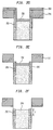
- the substrate includes a partially completed trench capacitor. For purposes of discussion, only the top portion of the trench capacitor is shown. The lower portion may be similar to the trench capacitor shown in FIG. 1.
- a collar 110 is provided in the upper portion of the trench capacitor, lining the trench sidewalls.
- the collar comprises, for example, dielectric material such as oxide formed from tetraethyloxosilane (TEOS).
- TEOS tetraethyloxosilane
- a nitride layer may be provided over the oxide collar to improve collar isolation characteristics.
- Poly 220 typically is used to fill the trench.
- the poly is doped with dopants. In one embodiment, the poly is doped with n-type dopants such as phosphorous (P) or arsenic (As). Alternatively, p-type dopants may be used for p-type array cells.
- the surface of the substrate is polished selective to the pad stop layer.
- the polish which for example comprises a chemical mechanical polish, polishes the poly at a faster rate than the material of the pad layer.
- the CMP removes the excess poly material from the surface without effectively removing the pad stop layer, producing a planar surface 227.
- an etch is performed to form a buried layer.
- the etch for example, comprises a reactive ion etch (RIE) selective to the pad stop and collar.
- RIE reactive ion etch
- the etch forms a recessed region 240 below surface 208 of the substrate.
- the etch recesses the poly in the trench to define a top surface 250 of the buried layer.
- subsequent processing may result in small amounts of materials being removed to further recess the trench, this removal of additional material is negligible.
- the etch effectively defines about the top surface of the buried layer.
- the depth of top of the surface buried strap depends on design requirements, such as isolation from a device layer located above the trench.
- the passing wordline is located above the trench.
- the distance between the top of the buried strap and the device layer should be large enough that the isolation material provides isolation between the two.
- the depth of the top surface of the buried strap is about 50 nm. The recess depth, or course, may vary and be optimized for specific applications to achieve the desired electrical characteristics.
- the dielectric collar above surface 250 is removed. Removal of the collar is achieved by, for example, an isotropic etch such as a wet of chemical dry etch. The etch is selective to the pad stop and poly.
- an over etch is performed to recess the collar below surface 250 to define the bottom of the buried layer. As a result, a recessed region 255 is provided below surface 250 that surrounds the trench.
- the over etch recesses the collar to a depth of about 50-100 nm below surface 250 to provide a buried strap layer thickness of about 50-100 nm.
- the depth of the over etch can vary depending on design requirements, such as resistance.
- a liner 260 is deposited to cover the surface of the pad stop layer, trench sidewalls, and surface 250.
- the liner comprises, in one embodiment, undoped silicon such as poly silicon or amorphous silicon. Germanium (Ge), carbon (C) or compounds including Ge-Si or Si-C compounds may also be used to form the liner.
- the liner is formed by conventional techniques such as, for example, LPCVD.
- the liner is sufficiently thick to fill the recessed region 255.
- the liner thickness depends on the thickness of the collar.
- the liner is at least half the thickness of the collar. Typically, the collar thickness is about 30 nm.
- a 20-40 nm thick liner is sufficient to fill the recessed region 25.
- the liner 260 comprises silicon deposited by selective epitaxial techniques. Such techniques are well known and are described in, for example, S.M. Sze, " VLSI Technology ", 2nd ed., New York, McGraw-Hill, 1988, which is herein incorporated by reference for all purposes. Selective epitaxial techniques advantageously deposit the liner on the trench sidewalls 20 and surface 250, filling recessed region 255.
- the excess material from the liner is removed, leaving liner material filling region 255. Removal of the excess liner material is achieved using, for example, an isotropic etch such as a wet etch or CDE. As a result, a buried layer 270 having thickness T is created.
- the epi layer is sufficiently thin such that the excess material lining trench sidewalls 20 and surface 250 are consumed by an thermal oxidation process, leaving recessed region filled with epi.
- the epi should be about 20-40 nm thick. This advantageously eliminates the etch used to remove the excess liner material.
- the oxidation process can either be a separate process or integrated as part of subsequent thermal processes during the fabrication of the IC.
- Processing continues to complete the IC. For example, defining the active region, forming a isolation in the non-active region, forming a transistor in the active region, and other processing to produce a DRAM cell as shown in FIG. 1. Interconnects may then be form, creating an IC which is packaged and used in electronic products.
Landscapes
- Engineering & Computer Science (AREA)
- Manufacturing & Machinery (AREA)
- Semiconductor Memories (AREA)
- Bipolar Transistors (AREA)
- Semiconductor Integrated Circuits (AREA)
Abstract
Description
Claims (1)
- A method for forming a buried layer comprising:providing a trench filled with semiconductor material in a substrate, the trench having a dielectric collar lining sidewalls of an upper portion of the trench, separating the semiconductor material from the trench sidewalls in the upper portion of the trench;recessing the semiconductor material below a surface of the substrate, the recess defines a top surface of the buried layer;recessing the collar below the top surface of the buried layer to create a recessed region surrounding the top surface of the semiconductor material, wherein a bottom surface of the recessed region defines a lower surface of the buried layer;depositing a liner to fill the recessed region; andremoving excess material from the liner the lines the sidewalls of the trench and top surface of the semiconductor material to leave the recessed region filled with the liner.
Applications Claiming Priority (2)
| Application Number | Priority Date | Filing Date | Title |
|---|---|---|---|
| US52683 | 1998-03-31 | ||
| US09/052,683 US6080618A (en) | 1998-03-31 | 1998-03-31 | Controllability of a buried device layer |
Publications (3)
| Publication Number | Publication Date |
|---|---|
| EP0948043A2 true EP0948043A2 (en) | 1999-10-06 |
| EP0948043A3 EP0948043A3 (en) | 2000-02-09 |
| EP0948043B1 EP0948043B1 (en) | 2003-08-13 |
Family
ID=21979225
Family Applications (1)
| Application Number | Title | Priority Date | Filing Date |
|---|---|---|---|
| EP99104721A Expired - Lifetime EP0948043B1 (en) | 1998-03-31 | 1999-03-10 | Method with improved controllability of a buried layer |
Country Status (7)
| Country | Link |
|---|---|
| US (1) | US6080618A (en) |
| EP (1) | EP0948043B1 (en) |
| JP (1) | JPH11312794A (en) |
| KR (1) | KR19990078429A (en) |
| CN (1) | CN1238899C (en) |
| DE (1) | DE69910293T2 (en) |
| TW (1) | TW404046B (en) |
Cited By (1)
| Publication number | Priority date | Publication date | Assignee | Title |
|---|---|---|---|---|
| WO2001075967A1 (en) * | 2000-03-30 | 2001-10-11 | Lam Research Corporation | In situ and ex situ etching process for sti with oxide collar application |
Families Citing this family (23)
| Publication number | Priority date | Publication date | Assignee | Title |
|---|---|---|---|---|
| US6074909A (en) * | 1998-07-31 | 2000-06-13 | Siemens Aktiengesellschaft | Apparatus and method for forming controlled deep trench top isolation layers |
| US6180480B1 (en) * | 1998-09-28 | 2001-01-30 | International Business Machines Corporation | Germanium or silicon-germanium deep trench fill by melt-flow process |
| GB9915589D0 (en) * | 1999-07-02 | 1999-09-01 | Smithkline Beecham Plc | Novel compounds |
| US6573137B1 (en) * | 2000-06-23 | 2003-06-03 | International Business Machines Corporation | Single sided buried strap |
| US6809368B2 (en) * | 2001-04-11 | 2004-10-26 | International Business Machines Corporation | TTO nitride liner for improved collar protection and TTO reliability |
| US6528367B1 (en) | 2001-11-30 | 2003-03-04 | Promos Technologies, Inc. | Self-aligned active array along the length direction to form un-biased buried strap formation for sub-150 NM BEST DRAM devices |
| US6759335B2 (en) | 2001-12-12 | 2004-07-06 | Promos Technologies, Inc. | Buried strap formation method for sub-150 nm best DRAM devices |
| KR100493025B1 (en) * | 2002-08-07 | 2005-06-07 | 삼성전자주식회사 | Method for manufacturing semiconductor memory device |
| FR2845522A1 (en) * | 2002-10-03 | 2004-04-09 | St Microelectronics Sa | INTEGRATED HIGHLY CONDUCTIVE LAYER CIRCUIT |
| KR100954416B1 (en) * | 2002-11-12 | 2010-04-26 | 매그나칩 반도체 유한회사 | Method for forming of capacitor the trench type |
| US7238588B2 (en) * | 2003-01-14 | 2007-07-03 | Advanced Micro Devices, Inc. | Silicon buffered shallow trench isolation |
| US6962857B1 (en) | 2003-02-05 | 2005-11-08 | Advanced Micro Devices, Inc. | Shallow trench isolation process using oxide deposition and anneal |
| US6673696B1 (en) * | 2003-01-14 | 2004-01-06 | Advanced Micro Devices, Inc. | Post trench fill oxidation process for strained silicon processes |
| US7422961B2 (en) * | 2003-03-14 | 2008-09-09 | Advanced Micro Devices, Inc. | Method of forming isolation regions for integrated circuits |
| US7648886B2 (en) * | 2003-01-14 | 2010-01-19 | Globalfoundries Inc. | Shallow trench isolation process |
| JP4483179B2 (en) * | 2003-03-03 | 2010-06-16 | 株式会社デンソー | Manufacturing method of semiconductor device |
| US6921709B1 (en) | 2003-07-15 | 2005-07-26 | Advanced Micro Devices, Inc. | Front side seal to prevent germanium outgassing |
| US7033885B2 (en) * | 2003-09-29 | 2006-04-25 | Nanya Technology Corporation | Deep trench structure manufacturing process |
| US7462549B2 (en) * | 2004-01-12 | 2008-12-09 | Advanced Micro Devices, Inc. | Shallow trench isolation process and structure with minimized strained silicon consumption |
| US7034352B2 (en) * | 2004-02-11 | 2006-04-25 | Infineon Technologies Ag | DRAM with very shallow trench isolation |
| US20060166433A1 (en) * | 2005-01-26 | 2006-07-27 | Min-Soo Kim | Recessed collar etch for buried strap window formation without poly2 |
| DE102005039667A1 (en) * | 2005-08-22 | 2007-03-01 | Infineon Technologies Ag | Producing a low aspect ratio structure and buried strap for a trench DRAM forms and fills trench in semiconductor substrate with initial and sacrificial layers and selectively removes especially at sidewalls |
| DE102007035832B4 (en) * | 2007-07-31 | 2012-03-29 | Globalfoundries Dresden Module One Limited Liability Company & Co. Kg | Method for producing an SOI semiconductor device and semiconductor device with trench capacitor |
Citations (3)
| Publication number | Priority date | Publication date | Assignee | Title |
|---|---|---|---|---|
| EP0794576A2 (en) * | 1996-03-04 | 1997-09-10 | Siemens Aktiengesellschaft | DRAM trench capacitor with insulating collar |
| EP0814507A1 (en) * | 1996-06-21 | 1997-12-29 | Siemens Aktiengesellschaft | Trench capacitor DRAM cell and method of making the same |
| EP0884785A2 (en) * | 1997-06-11 | 1998-12-16 | Siemens Aktiengesellschaft | Trench capacitor dram cell with vertical transistor |
Family Cites Families (2)
| Publication number | Priority date | Publication date | Assignee | Title |
|---|---|---|---|---|
| US5389559A (en) * | 1993-12-02 | 1995-02-14 | International Business Machines Corporation | Method of forming integrated interconnect for very high density DRAMs |
| US5395786A (en) * | 1994-06-30 | 1995-03-07 | International Business Machines Corporation | Method of making a DRAM cell with trench capacitor |
-
1998
- 1998-03-31 US US09/052,683 patent/US6080618A/en not_active Expired - Fee Related
-
1999
- 1999-03-09 TW TW088103608A patent/TW404046B/en active
- 1999-03-10 EP EP99104721A patent/EP0948043B1/en not_active Expired - Lifetime
- 1999-03-10 DE DE69910293T patent/DE69910293T2/en not_active Expired - Fee Related
- 1999-03-29 JP JP11086314A patent/JPH11312794A/en not_active Withdrawn
- 1999-03-31 CN CNB991046188A patent/CN1238899C/en not_active Expired - Fee Related
- 1999-03-31 KR KR1019990011139A patent/KR19990078429A/en not_active Application Discontinuation
Patent Citations (3)
| Publication number | Priority date | Publication date | Assignee | Title |
|---|---|---|---|---|
| EP0794576A2 (en) * | 1996-03-04 | 1997-09-10 | Siemens Aktiengesellschaft | DRAM trench capacitor with insulating collar |
| EP0814507A1 (en) * | 1996-06-21 | 1997-12-29 | Siemens Aktiengesellschaft | Trench capacitor DRAM cell and method of making the same |
| EP0884785A2 (en) * | 1997-06-11 | 1998-12-16 | Siemens Aktiengesellschaft | Trench capacitor dram cell with vertical transistor |
Cited By (2)
| Publication number | Priority date | Publication date | Assignee | Title |
|---|---|---|---|---|
| WO2001075967A1 (en) * | 2000-03-30 | 2001-10-11 | Lam Research Corporation | In situ and ex situ etching process for sti with oxide collar application |
| US6649996B2 (en) | 2000-03-30 | 2003-11-18 | Lam Research Corporation | In situ and ex situ hardmask process for STI with oxide collar application |
Also Published As
| Publication number | Publication date |
|---|---|
| DE69910293D1 (en) | 2003-09-18 |
| CN1248797A (en) | 2000-03-29 |
| TW404046B (en) | 2000-09-01 |
| DE69910293T2 (en) | 2004-06-09 |
| US6080618A (en) | 2000-06-27 |
| EP0948043A3 (en) | 2000-02-09 |
| KR19990078429A (en) | 1999-10-25 |
| CN1238899C (en) | 2006-01-25 |
| JPH11312794A (en) | 1999-11-09 |
| EP0948043B1 (en) | 2003-08-13 |
Similar Documents
| Publication | Publication Date | Title |
|---|---|---|
| EP0948043B1 (en) | Method with improved controllability of a buried layer | |
| US6163045A (en) | Reduced parasitic leakage in semiconductor devices | |
| US6018174A (en) | Bottle-shaped trench capacitor with epi buried layer | |
| US5945704A (en) | Trench capacitor with epi buried layer | |
| EP1199745B1 (en) | Method of forming vertical transistor trench capacitor DRAM with SOI logic devices | |
| US5065273A (en) | High capacity DRAM trench capacitor and methods of fabricating same | |
| US6806137B2 (en) | Trench buried bit line memory devices and methods thereof | |
| US6426253B1 (en) | Method of forming a vertically oriented device in an integrated circuit | |
| US6008513A (en) | Dynamic random access memory (DRAM) cells with minimum active cell areas using sidewall-space bit lines | |
| US20050285175A1 (en) | Vertical SOI Device | |
| US6309924B1 (en) | Method of forming self-limiting polysilicon LOCOS for DRAM cell | |
| US7157329B2 (en) | Trench capacitor with buried strap | |
| US5867420A (en) | Reducing oxidation stress in the fabrication of devices | |
| US6265741B1 (en) | Trench capacitor with epi buried layer | |
| JPH11330403A (en) | Manufacture of trench capacitor | |
| US6124206A (en) | Reduced pad erosion | |
| EP0884785B1 (en) | Trench capacitor dram cell with vertical transistor | |
| US6812091B1 (en) | Trench capacitor memory cell | |
| US20020167045A1 (en) | Increase in deep trench capacitance by a central ground electrode | |
| EP0905783B1 (en) | Vertical transistor implemented in a memory cell comprising a trench capacitor | |
| US20020130346A1 (en) | Structure and process for buried bitline and single sided buried conductor formation |
Legal Events
| Date | Code | Title | Description |
|---|---|---|---|
| PUAI | Public reference made under article 153(3) epc to a published international application that has entered the european phase |
Free format text: ORIGINAL CODE: 0009012 |
|
| AK | Designated contracting states |
Kind code of ref document: A2 Designated state(s): DE FR GB IE IT NL |
|
| AX | Request for extension of the european patent |
Free format text: AL;LT;LV;MK;RO;SI |
|
| PUAL | Search report despatched |
Free format text: ORIGINAL CODE: 0009013 |
|
| AK | Designated contracting states |
Kind code of ref document: A3 Designated state(s): AT BE CH CY DE DK ES FI FR GB GR IE IT LI LU MC NL PT SE |
|
| AX | Request for extension of the european patent |
Free format text: AL;LT;LV;MK;RO;SI |
|
| RIC1 | Information provided on ipc code assigned before grant |
Free format text: 7H 01L 21/8242 A, 7H 01L 21/74 B |
|
| 17P | Request for examination filed |
Effective date: 20000330 |
|
| AKX | Designation fees paid |
Free format text: DE FR GB IE IT NL |
|
| 17Q | First examination report despatched |
Effective date: 20001016 |
|
| GRAH | Despatch of communication of intention to grant a patent |
Free format text: ORIGINAL CODE: EPIDOS IGRA |
|
| GRAH | Despatch of communication of intention to grant a patent |
Free format text: ORIGINAL CODE: EPIDOS IGRA |
|
| GRAA | (expected) grant |
Free format text: ORIGINAL CODE: 0009210 |
|
| RAP1 | Party data changed (applicant data changed or rights of an application transferred) |
Owner name: INFINEON TECHNOLOGIES AG |
|
| AK | Designated contracting states |
Designated state(s): DE FR GB IE IT NL |
|
| REG | Reference to a national code |
Ref country code: GB Ref legal event code: FG4D |
|
| REG | Reference to a national code |
Ref country code: IE Ref legal event code: FG4D |
|
| REF | Corresponds to: |
Ref document number: 69910293 Country of ref document: DE Date of ref document: 20030918 Kind code of ref document: P |
|
| ET | Fr: translation filed | ||
| PLBE | No opposition filed within time limit |
Free format text: ORIGINAL CODE: 0009261 |
|
| STAA | Information on the status of an ep patent application or granted ep patent |
Free format text: STATUS: NO OPPOSITION FILED WITHIN TIME LIMIT |
|
| 26N | No opposition filed |
Effective date: 20040514 |
|
| REG | Reference to a national code |
Ref country code: HK Ref legal event code: WD Ref document number: 1019961 Country of ref document: HK |
|
| REG | Reference to a national code |
Ref country code: GB Ref legal event code: 713A Free format text: APPLICATION FOR INVENTOR TO BE MENTIONED UNDER SECTION 13(1) |
|
| PGFP | Annual fee paid to national office [announced via postgrant information from national office to epo] |
Ref country code: NL Payment date: 20060314 Year of fee payment: 8 |
|
| REG | Reference to a national code |
Ref country code: GB Ref legal event code: 713F |
|
| REG | Reference to a national code |
Ref country code: FR Ref legal event code: RM |
|
| PGFP | Annual fee paid to national office [announced via postgrant information from national office to epo] |
Ref country code: GB Payment date: 20070322 Year of fee payment: 9 |
|
| NLV4 | Nl: lapsed or anulled due to non-payment of the annual fee |
Effective date: 20071001 |
|
| PG25 | Lapsed in a contracting state [announced via postgrant information from national office to epo] |
Ref country code: NL Free format text: LAPSE BECAUSE OF NON-PAYMENT OF DUE FEES Effective date: 20071001 |
|
| PGFP | Annual fee paid to national office [announced via postgrant information from national office to epo] |
Ref country code: IT Payment date: 20080326 Year of fee payment: 10 Ref country code: IE Payment date: 20080321 Year of fee payment: 10 |
|
| PGFP | Annual fee paid to national office [announced via postgrant information from national office to epo] |
Ref country code: FR Payment date: 20080314 Year of fee payment: 10 Ref country code: DE Payment date: 20080510 Year of fee payment: 10 |
|
| GBPC | Gb: european patent ceased through non-payment of renewal fee |
Effective date: 20080310 |
|
| PG25 | Lapsed in a contracting state [announced via postgrant information from national office to epo] |
Ref country code: GB Free format text: LAPSE BECAUSE OF NON-PAYMENT OF DUE FEES Effective date: 20080310 |
|
| REG | Reference to a national code |
Ref country code: FR Ref legal event code: ST Effective date: 20091130 |
|
| REG | Reference to a national code |
Ref country code: IE Ref legal event code: MM4A |
|
| PG25 | Lapsed in a contracting state [announced via postgrant information from national office to epo] |
Ref country code: IE Free format text: LAPSE BECAUSE OF NON-PAYMENT OF DUE FEES Effective date: 20090310 Ref country code: DE Free format text: LAPSE BECAUSE OF NON-PAYMENT OF DUE FEES Effective date: 20091001 |
|
| PG25 | Lapsed in a contracting state [announced via postgrant information from national office to epo] |
Ref country code: FR Free format text: LAPSE BECAUSE OF NON-PAYMENT OF DUE FEES Effective date: 20091123 |
|
| PG25 | Lapsed in a contracting state [announced via postgrant information from national office to epo] |
Ref country code: IT Free format text: LAPSE BECAUSE OF NON-PAYMENT OF DUE FEES Effective date: 20090310 |