EP0942465A2 - Self aligned buried plate - Google Patents
Self aligned buried plate Download PDFInfo
- Publication number
- EP0942465A2 EP0942465A2 EP99103856A EP99103856A EP0942465A2 EP 0942465 A2 EP0942465 A2 EP 0942465A2 EP 99103856 A EP99103856 A EP 99103856A EP 99103856 A EP99103856 A EP 99103856A EP 0942465 A2 EP0942465 A2 EP 0942465A2
- Authority
- EP
- European Patent Office
- Prior art keywords
- trench
- layer
- polysilicon layer
- silicon substrate
- etching
- Prior art date
- Legal status (The legal status is an assumption and is not a legal conclusion. Google has not performed a legal analysis and makes no representation as to the accuracy of the status listed.)
- Withdrawn
Links
- 238000000034 method Methods 0.000 claims abstract description 163
- 229910021420 polycrystalline silicon Inorganic materials 0.000 claims abstract description 133
- 229920005591 polysilicon Polymers 0.000 claims abstract description 133
- 150000004767 nitrides Chemical class 0.000 claims abstract description 92
- XUIMIQQOPSSXEZ-UHFFFAOYSA-N Silicon Chemical compound [Si] XUIMIQQOPSSXEZ-UHFFFAOYSA-N 0.000 claims abstract description 89
- 229910052710 silicon Inorganic materials 0.000 claims abstract description 89
- 239000010703 silicon Substances 0.000 claims abstract description 89
- 238000005530 etching Methods 0.000 claims abstract description 62
- 239000000758 substrate Substances 0.000 claims abstract description 51
- 239000000463 material Substances 0.000 claims description 87
- 239000003990 capacitor Substances 0.000 claims description 58
- 229910052785 arsenic Inorganic materials 0.000 claims description 53
- RQNWIZPPADIBDY-UHFFFAOYSA-N arsenic atom Chemical compound [As] RQNWIZPPADIBDY-UHFFFAOYSA-N 0.000 claims description 53
- 238000005229 chemical vapour deposition Methods 0.000 claims description 7
- 238000004518 low pressure chemical vapour deposition Methods 0.000 claims description 7
- 238000001312 dry etching Methods 0.000 claims description 3
- 239000010410 layer Substances 0.000 description 246
- 235000012431 wafers Nutrition 0.000 description 101
- BOTDANWDWHJENH-UHFFFAOYSA-N Tetraethyl orthosilicate Chemical compound CCO[Si](OCC)(OCC)OCC BOTDANWDWHJENH-UHFFFAOYSA-N 0.000 description 25
- 238000000059 patterning Methods 0.000 description 21
- 230000003647 oxidation Effects 0.000 description 13
- 238000007254 oxidation reaction Methods 0.000 description 13
- 230000001681 protective effect Effects 0.000 description 12
- 239000005388 borosilicate glass Substances 0.000 description 9
- 238000004519 manufacturing process Methods 0.000 description 8
- 238000000137 annealing Methods 0.000 description 7
- 238000000151 deposition Methods 0.000 description 6
- 230000008021 deposition Effects 0.000 description 5
- 239000002019 doping agent Substances 0.000 description 5
- 230000015654 memory Effects 0.000 description 5
- XKRFYHLGVUSROY-UHFFFAOYSA-N Argon Chemical compound [Ar] XKRFYHLGVUSROY-UHFFFAOYSA-N 0.000 description 4
- 239000004065 semiconductor Substances 0.000 description 4
- 239000011248 coating agent Substances 0.000 description 3
- 238000000576 coating method Methods 0.000 description 3
- 229920002120 photoresistant polymer Polymers 0.000 description 3
- 238000001039 wet etching Methods 0.000 description 3
- 229910052786 argon Inorganic materials 0.000 description 2
- 238000007796 conventional method Methods 0.000 description 2
- 230000007547 defect Effects 0.000 description 2
- 230000002950 deficient Effects 0.000 description 2
- PEDCQBHIVMGVHV-UHFFFAOYSA-N glycerol Substances OCC(O)CO PEDCQBHIVMGVHV-UHFFFAOYSA-N 0.000 description 2
- 230000005055 memory storage Effects 0.000 description 2
- 230000001590 oxidative effect Effects 0.000 description 2
- 239000000047 product Substances 0.000 description 2
- 239000011241 protective layer Substances 0.000 description 2
- 238000009279 wet oxidation reaction Methods 0.000 description 2
- XPDWGBQVDMORPB-UHFFFAOYSA-N Fluoroform Chemical compound FC(F)F XPDWGBQVDMORPB-UHFFFAOYSA-N 0.000 description 1
- OAICVXFJPJFONN-UHFFFAOYSA-N Phosphorus Chemical compound [P] OAICVXFJPJFONN-UHFFFAOYSA-N 0.000 description 1
- 230000001413 cellular effect Effects 0.000 description 1
- 238000005137 deposition process Methods 0.000 description 1
- 238000005516 engineering process Methods 0.000 description 1
- 239000012467 final product Substances 0.000 description 1
- 239000011521 glass Substances 0.000 description 1
- BHEPBYXIRTUNPN-UHFFFAOYSA-N hydridophosphorus(.) (triplet) Chemical compound [PH] BHEPBYXIRTUNPN-UHFFFAOYSA-N 0.000 description 1
- 238000009740 moulding (composite fabrication) Methods 0.000 description 1
- UPSOBXZLFLJAKK-UHFFFAOYSA-N ozone;tetraethyl silicate Chemical compound [O-][O+]=O.CCO[Si](OCC)(OCC)OCC UPSOBXZLFLJAKK-UHFFFAOYSA-N 0.000 description 1
- 229910052698 phosphorus Inorganic materials 0.000 description 1
- 239000011574 phosphorus Substances 0.000 description 1
- 238000001020 plasma etching Methods 0.000 description 1
- 239000000376 reactant Substances 0.000 description 1
- 230000001360 synchronised effect Effects 0.000 description 1
- 239000012808 vapor phase Substances 0.000 description 1
Images


Classifications
-
- H—ELECTRICITY
- H01—ELECTRIC ELEMENTS
- H01L—SEMICONDUCTOR DEVICES NOT COVERED BY CLASS H10
- H01L21/00—Processes or apparatus adapted for the manufacture or treatment of semiconductor or solid state devices or of parts thereof
- H01L21/70—Manufacture or treatment of devices consisting of a plurality of solid state components formed in or on a common substrate or of parts thereof; Manufacture of integrated circuit devices or of parts thereof
-
- H—ELECTRICITY
- H01—ELECTRIC ELEMENTS
- H01L—SEMICONDUCTOR DEVICES NOT COVERED BY CLASS H10
- H01L29/00—Semiconductor devices adapted for rectifying, amplifying, oscillating or switching, or capacitors or resistors with at least one potential-jump barrier or surface barrier, e.g. PN junction depletion layer or carrier concentration layer; Details of semiconductor bodies or of electrodes thereof ; Multistep manufacturing processes therefor
- H01L29/66—Types of semiconductor device ; Multistep manufacturing processes therefor
- H01L29/66007—Multistep manufacturing processes
- H01L29/66075—Multistep manufacturing processes of devices having semiconductor bodies comprising group 14 or group 13/15 materials
- H01L29/66083—Multistep manufacturing processes of devices having semiconductor bodies comprising group 14 or group 13/15 materials the devices being controllable only by variation of the electric current supplied or the electric potential applied, to one or more of the electrodes carrying the current to be rectified, amplified, oscillated or switched, e.g. two-terminal devices
- H01L29/66181—Conductor-insulator-semiconductor capacitors, e.g. trench capacitors
-
- H—ELECTRICITY
- H01—ELECTRIC ELEMENTS
- H01L—SEMICONDUCTOR DEVICES NOT COVERED BY CLASS H10
- H01L29/00—Semiconductor devices adapted for rectifying, amplifying, oscillating or switching, or capacitors or resistors with at least one potential-jump barrier or surface barrier, e.g. PN junction depletion layer or carrier concentration layer; Details of semiconductor bodies or of electrodes thereof ; Multistep manufacturing processes therefor
- H01L29/66—Types of semiconductor device ; Multistep manufacturing processes therefor
- H01L29/86—Types of semiconductor device ; Multistep manufacturing processes therefor controllable only by variation of the electric current supplied, or only the electric potential applied, to one or more of the electrodes carrying the current to be rectified, amplified, oscillated or switched
- H01L29/92—Capacitors with potential-jump barrier or surface barrier
- H01L29/94—Metal-insulator-semiconductors, e.g. MOS
- H01L29/945—Trench capacitors
-
- H—ELECTRICITY
- H10—SEMICONDUCTOR DEVICES; ELECTRIC SOLID-STATE DEVICES NOT OTHERWISE PROVIDED FOR
- H10B—ELECTRONIC MEMORY DEVICES
- H10B12/00—Dynamic random access memory [DRAM] devices
- H10B12/01—Manufacture or treatment
- H10B12/02—Manufacture or treatment for one transistor one-capacitor [1T-1C] memory cells
- H10B12/03—Making the capacitor or connections thereto
- H10B12/038—Making the capacitor or connections thereto the capacitor being in a trench in the substrate
- H10B12/0387—Making the trench
-
- H—ELECTRICITY
- H10—SEMICONDUCTOR DEVICES; ELECTRIC SOLID-STATE DEVICES NOT OTHERWISE PROVIDED FOR
- H10B—ELECTRONIC MEMORY DEVICES
- H10B12/00—Dynamic random access memory [DRAM] devices
- H10B12/30—DRAM devices comprising one-transistor - one-capacitor [1T-1C] memory cells
- H10B12/37—DRAM devices comprising one-transistor - one-capacitor [1T-1C] memory cells the capacitor being at least partially in a trench in the substrate
Definitions
- the present invention relates generally to the manufacture of integrated circuits (ICs). More specifically, the invention relates to a method of manufacturing self aligned buried plates within a deep trench formed into a silicon substrate.
- Buried plate structures formed within deep trenches that are etched into a silicon substrate are commonly used in the integrated circuit industry. These buried plate structures may be used to, for example, form integrated circuit components such as trench capacitors that may be used as memory storage nodes in devices such as DRAMs.
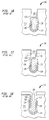
- the conventional vertical patterning processes used to produce these buried plates are relatively complex and, as described in more detail below, are not self-aligning. In order to more clearly illustrate these problems, a prior art process for producing a trench capacitor on a silicon wafer will be described with reference to Figures 1-19.
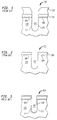
- a silicon wafer 100 is provided having a deep trench 102 etched into wafer 100.
- Wafer 100 typically has a thin pad oxide layer 104 and a pad nitride layer 106 formed on a top surface 108 of a silicon substrate 110.
- pad oxide layer 104 acts as a stress relieving layer for preventing pad nitride layer 106 from separating from silicon substrate 110 during subsequent high temperature process steps.
- Pad nitride layer 106 which is typically about 200 angstroms thick, acts as a protective layer for top surface 108 of substrate 110 during subsequent process steps such as oxidation steps.
- trench 102 is formed into wafer 100 using a deep trench etching process.
- a Borosilicate glass (BSG) hard mask layer 112 is applied over pad nitride layer 106.
- BSG hard mask 112 is then patterned with a resist material (not shown) and etched using a conventional hard mask etching process such as a dry etch process using an CF 4 /CF 3 /Argon etchant.
- a conventional hard mask etching process such as a dry etch process using an CF 4 /CF 3 /Argon etchant.
- One or more etching process opens BSG hard mask layer 112 (as well as pad nitride layer 106 and pad oxide layer 104) in the areas above where deep trench 102 is to be etched.
- the resist material (not shown) used to pattern hard mask 112 is then removed using well known resist removing processes.
- Deep trench 102 is then etched using an appropriate etching process such as a dry etch using an HBr/NH 3 /O 2 etchant.
- the deep trench is etched to a level of about 8 microns below top surface 108 of silicon substrate 110 forming trench sidewalls 114 and 116.
- BSG hard mask layer 112 is removed using any conventional hard mask removal process such as, for example, a vapor phase etching process using HF vapor. At this point the process steps used to form a buried plate structure within the deep trench begins.
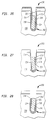
- the first step in actually forming a conventional buried plate structure involves depositing an arsenic doped silicon tetrethylorthosilicate glass (ASG TEOS) layer 118 over pad nitride layer 106 and over the surfaces of trench 102.
- ASG TEOS layer 116 is used to provide the arsenic doping for certain regions of silicon substrate 100 during subsequent annealing steps.
- This layer may be applied using a conventional chemical vapor deposition (CVD) technique and is typically applied at a thickness of, for example, about 40-60 nm.
- CVD chemical vapor deposition
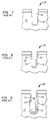
- ASG TEOS layer 116 is etched from the top surface of the pad nitride layer and from certain uppermost portions of trench sidewalls 114, and 116 of trench, 102. This etching process is accomplished using the process steps illustrated in Figures 4-7.
- a resist material 120 is first applied to wafer 100. This resist material fills trench 102 and coats the top surface of wafer 100 with a layer of resist material.
- resist material 120 is recessed or etched back to a desired level within trench 102, in this case, to a level in the range of about 5.5 to 6.5 microns above the bottom of trench 102. This etching back of the resist exposes portions of the ASG TEOS layer at the uppermost portions of the sidewalls 114 and 116 of trench 102.
- This step is accomplished using a conventional photoresist etching process. As described in more detail hereinafter, this is the step that determines the level of the first vertical patterning step for this process.
- ASG TEOS layer 118 is etched away from the top of wafer 100 and from the exposed portions of sidewalls 114 and 116.
- a wet etching process using, for example, a BHF etchant is typically used to etch, and slightly over etch, the ASG TEOS layer.
- ASG TEOS layer 118 may be slightly recessed below the level of the remaining resist as shown in Figure 6.
- this etching process is finished by removing the remaining portions of resist material 120 using a conventional photoresist removal process. Once the resist is removed, only portions of ASG TEOS layer 118 remain with these portions covering the bottom portions of trench 102.
- the ASG TEOS layer is annealed as illustrated in Figures 8-10. This annealing process produces an arsenic doped region within silicon substrate 110 surrounding the bottom portions of trench 102. This arsenic doped region forms the buried plate structure. In the specific case of a trench capacitor that is being described, this arsenic doped region forms one of the plates of the capacitor.
- Cap TEOS layer 122 is deposited over wafer 100 coating trench 102 as illustrated in Figure 8.
- Cap TEOS layer 122 is an undoped TEOS or ozone TEOS layer that prevents the arsenic doped TEOS 118 from doping the upper portions of trench sidewalls 114 and 116 and/or to prevent the arsenic dopant from escaping from the trench during the dopant drive anneal step.
- Cap TEOS layer 122 is applied using a conventional CVD technique and is typically applied at a thickness of, for example, about 400 Angstroms.
- wafer 100 is annealed. During the annealing step, the temperature is elevated for an specific length of time. In this specific case, the temperature is raised to about 1050 degrees F for a period of about 30 minutes. This high temperature moves the arsenic from ASG TEOS layer 118 into the surrounding region of silicon substrate 110 thereby forming a buried plate structure 124 within a region of silicon substrate 110 surrounding the bottom portion of trench 102. This process is illustrated in Figure 9. After the annealing step, the remaining portions of ASG TEOS layer 118 and cap TEOS layer 122 are removed. This is accomplished using a conventional process such as, for example a wet etching process using, for example, a BHF etchant.
- a conventional process such as, for example a wet etching process using, for example, a BHF etchant.
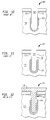
- a nitride layer is formed on the trench walls adjacent to buried plate structure 124 using the process steps illustrated in Figures 11-15.
- This nitride layer acts as a dielectric for the trench capacitor.
- This process of forming the capacitor dielectric is the second vertical patterning step of the overall process of forming the trench capacitor. As will be described in more detail hereinafter, this second vertical patterning step must be strictly controlled so that the top of the nitride layer is at the proper level relative to buried plate structure 124. Because two separate vertical patterning steps are used to locate the top of the nitride layer relative to the top of buried plate structure 124, these layers are not self-aligned.
- nitride layer 126 is deposited over wafer 100 coating trench sidewalls 114 and 116.
- Nitride layer 126 is formed using a conventional low pressure chemical vapor deposition process and is about, for example, 7 nm thick.
- nitride layer 126 may be reoxidized at this stage using a wet oxidation process. This reoxidizing step reduces any defects in nitride layer 126 by filling any holes with oxide and improves the dielectric properties of nitride layer 126.
- an arsenic doped polysilicon material 128 is applied over wafer 100 so that it fills trench 102 as illustrated in Figure 12.
- Arsenic doped polysilicon material 128 is typically formed using a layering process in which a layer of undoped polysilicon is laid down, then a layer of arsenic, and then another layer of undoped polysilicon in order to form overall layer 128. These alternating layers, which are not shown in the Figures, are mixed in subsequent high temperature oxide forming steps.
- a conventional planarization step such as chemical-mechanical polish (CMP) is performed which removes polysilicon material 128 from the top surface of wafer 100.
- CMP chemical-mechanical polish
- polysilicon material 128 is recessed or etched to a desired level within trench 102.
- Polysilicon material 128 is typically etched using a conventional dry etch process such as a reactive ion etching process using SF 6 as the reactant. As described briefly above, this etching step is very important because it determines the vertical alignment of the nitride layer relative to the previously formed buried plate structure 124. Therefore, it is critical that this etch process removes the polysilicon material 128 down to a level just slightly below the level of the top of buried plate structure 124 as illustrated in Figure 14. For example, in this case, the polysilicon material is etched down to a level of about 100 nm below the uppermost portion of the buried plate structure 124. If these two vertically positioned layers are not properly aligned, the trench capacitor may not be able to hold its charge properly resulting in a defective memory cell.
- nitride layer 126 and any exposed reoxidized nitride are etched away from the top surface of wafer 100 and from the uppermost portions of trench sidewalls 114 and 116 as illustrated in Figure 15.
- This step uses a conventional nitride etching process such as, for example, a wet etch process using, for example, an HF-glycerol etchant.
- This nitride etching step exposes silicon substrate 100 at the uppermost portions of trench sidewalls 114 and 116 and completes the process of forming the nitride dielectric layer for the trench capacitor.
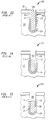
- the next process involved in forming the trench capacitor is the process of forming a protective oxide layer on the exposed uppermost portions of trench sidewalls 114 and 116.
- the protective oxide layer is a two layer structure formed using the steps shown in Figures 16-18.
- the protective oxide layer is used to cover the exposed silicon substrate 100 at the uppermost portions of trench sidewalls 114 and 116, cover the exposed edge of nitride layer 126, and isolate the buried plate structure 124 from the arsenic doped polysilicon 128 which is already in trench 102 as well as additional arsenic doped polysilicon material that will be added in a subsequent process step.
- the high temperature steps associated with forming the protective oxide layer are used to mix the arsenic doped polysilicon material 128.
- the first step in forming the protective oxide layer involves performing a collar oxide forming step. This is done using a conventional collar oxidation process such as a dry oxidation process to form a thin collar oxide layer 130. Collar oxide layer 130 is formed on the exposed uppermost trench sidewalls 114 and 116. However, since the top surface of polysilicon material 128 is also exposed during the collar oxidizing step, collar oxide layer 130 is also formed over the top of polysilicon material 128 as illustrated in Figure 16. In this case, collar oxide layer 130 is formed to be about 8 nm thick on trench sidewalls 114 and 116. Also, since the collar oxidation step is a high temperature step, this step begins to mix the arsenic and polysilicon making up arsenic doped polysilicon material 128.
- collar oxide deposition layer 132 of collar oxide is deposited over wafer 100 such that it coats the unfilled portions of trench 102 as illustrated in Figure 17.
- collar oxide deposition layer 132 is deposited at a thickness ranging from about 30 nm to about 45 nm. The thickness varies depending on the location on wafer 100 because of the varying contours of the wafer. For example, collar oxide deposition layer 132 may be about 45 nm thick on the top surface of wafer 100 and about 30 nm thick on trench sidewalls 114 and 116.
- Collar oxide deposition layer 132 is applied using a conventional collar oxide deposition process such as a plasma enhanced TEOS process.
- this step includes a 20 minute anneal at a temperature of about 1000 degrees F.
- This anneal step typically slightly thins collar oxide layer 132.
- this high temperature anneal step further mixes the arsenic and the polysilicon that makes up arsenic doped polysilicon material 128.
- the final step in forming the protective oxide layer is illustrated in Figure 18.
- This step involves etching away the collar oxide layers from the top of polysilicon material 128 and the top of wafer 100.
- a conventional oxide etching process such as a dry etch process using a CHF 3 /He/O 2 etchant is used to etch the collar oxide layers.
- This etching step is important because it is critical to make sure that substantially all of the collar oxide layers 130 and 132 are removed from the top of polysilicon material 128 within trench 102. If all of the collar oxide material is not removed, it may cause electrical resistance between the arsenic doped polysilicon material 128 in the bottom of trench 102 and the arsenic doped polysilicon material that is placed over the top of material 128 as described immediately below. This electrical resistance may interfere with the proper functioning of the trench capacitor.
- the final step in forming the trench capacitor is the step of applying another layer of arsenic doped polysilicon material 134 such that it fills the remaining unfilled portions of trench 102 as illustrated in Figure 19.
- Arsenic doped polysilicon layer 134 may be applied in the same multi-layer manner as described above for arsenic doped polysilicon material 128. If this is the case, the arsenic and the polysilicon would be mixed in subsequent process steps that will not be described herein.
- the first vertical patterning step is illustrated best in Figure 5. This step determines the height within the trench at which the top of the buried plate structure 124 will be located.
- the second vertical patterning step is best illustrated in Figure 14. This is the step which determines the height within the trench at which the top of nitride dielectric layer 126 will be located. This step also determines the height within the trench at which the bottom edge of the protective oxide layers 130 and 132 will be vertically located. Because the vertical location of the top of the buried plate structure 124 and the vertical location of the top of the nitride layer 126 are determined in two separate process steps, this overall process is not self-aligning.
- these two vertical patterning steps must be very closely controlled to insure that theses two layers are properly aligned. This is a difficult process and results in a high cost for producing trench capacitors using this approach. If these vertical layers are not properly aligned, the capacitor may not be able to properly hold its charge resulting in a defective capacitor.
- the above described process is a complex process including a large number of individual process steps. This large number of steps in itself makes the process expensive and time consuming.
- the above described process includes multiple high temperature anneal steps. These steps consumes more of the available temperature budget, are time consuming and therefore reduce the throughput of the manufacturing process making the process more costly.
- the collar oxide step is important because it is critical to make sure that substantially all of the collar oxide layers 130 and 132 are removed from the top of polysilicon material 128 within trench 102. If all of the collar oxide material is not removed, it may cause electrical resistance problems between the arsenic doped polysilicon material 128 in the bottom of trench 102 and the arsenic doped polysilicon material 134 that is placed over the top of material 128. This electrical resistance may interfere with the proper functioning of the trench capacitor.
- the top surface of polysilicon material 128 on which the oxide layers are formed should be as level or flat as possible. If there is a substantial concave or V shape to this top surface, the thickness of the collar oxide layers may vary dramatically making it difficult to properly etch all of the collar oxide material from the top surface of polysilicon material 128.
- deep trench 102 may be formed with slightly tapered trench sidewalls. That is, trench 102 is wider at the top of the trench and narrower at the bottom of the trench. This helps ensure that the etching process used to etch back polysilicon material 128 results in a flat and level top surface for the remaining polysilicon material 128.
- the use of a tapered trench with a narrower bottom than top causes the capacitance of the trench capacitor formed using the above described process to be less than the capacitance that would be possible if trenches having vertical sidewalls were used.
- a method of forming a buried plate in a silicon substrate having a deep trench etched into the silicon substrate is herein disclosed.
- the trench has sidewalls defining the depth of the trench.
- the method includes the step of forming a highly doped polysilicon layer within the trench.
- a nitride layer is then formed within the trench over the polysilicon layer.
- both the polysilicon layer and the nitride layer are etched from a certain uppermost portion of the sidewalls of the trench thereby exposing the silicon substrate at the uppermost portions of the sidewalls.
- a collar oxide layer is formed over the exposed silicon substrate at the uppermost portions of the sidewalls thereby protecting any edges of the polysilicon layer exposed by the etching step.
- the method further includes the step of forming a thin thermal oxide layer within the trench prior to forming the highly doped polysilicon layer.
- the thin thermal oxide layer is approximately about 15 angstroms thick.
- the highly doped polysilicon layer is doped with arsenic.
- the concentration of the arsenic in the polysilicon layer is greater than about 5E 19 /cm 3
- the polysilicon layer is approximately about 300 angstroms thick
- the polysilicon layer is formed using a chemical vapor deposition process.
- the nitride layer is approximately about 6 nm thick and the nitride layer is formed using a low pressure chemical vapor deposition process.
- the step of etching the polysilicon layer and the nitride layer includes several steps. Before etching the polysilicon layer and the nitride layer, the trench is filled with a resist material. The resist material is then recessed to a certain level within the trench. The nitride layer and the polysilicon layer are then etched with the thermal oxide layer acting as an etch stop. The thermal oxide layer is then etched to expose the silicon substrate at the uppermost portions of the sidewalls of the trench. And finally, any remaining resist material is removed from the trench. In one version of this embodiment, the trench is formed approximately about 8 microns deep within the silicon substrate and the resist material is recessed to a level of approximately about 5.5 to 6.5 microns above the bottom of the trench.
- the method is used to form a trench capacitor in a silicon substrate for use in a DRAM device.
- the portions of the polysilicon layer that remain after the etching step are used to form a buried plate forming part of the trench capacitor.
- the portions of the nitride layer that remain after the etching step are used to form a dielectric layer for the trench capacitor.
- the trench is filed with doped polysilicon after the step of forming the collar oxide. Portions of the doped polysilicon fill act as a second plate for the trench capacitor.
- An invention is herein described for providing methods for manufacturing a trench capacitor within a deep trench formed into a semiconductor wafer, such as a silicon wafer.
- the trench capacitor is used in integrated circuits (ICs) including memory ICs such as random access memories (RAMs), dynamic random access memories (DRAMs), synchronous DRAMs (SDRAMs), merged DRAM-logic circuits (embedded DRAMs), or other circuits.
- ICs integrated circuits
- RAMs random access memories
- DRAMs dynamic random access memories
- SDRAMs synchronous DRAMs
- merged DRAM-logic circuits embedded DRAMs
- ICs are formed on the wafer in parallel. After processing is finish, the wafer is diced to separate the integrated circuits to individual chips. The chips are then packaged, resulting in a final product that is used in, for example, consumer products such as computer systems, cellular phones, personal digital assistants (PDAs), and other electronic products.
- PDAs personal digital assistants
- the invention utilizes fewer vertical patterning steps which makes the process self-aligning thereby eliminating the problems associated with controlling the vertical alignment of various layers of the trench capacitor formed during different vertical patterning steps.
- the present invention will be described using the example of a trench capacitor formed into a deep trench within a silicon wafer.
- the trench capacitor is used as a memory storage node of a DRAM device.
- this example shows specific elements positioned at specific dimensional locations, it should be understood that the present invention is not limited to this specific configuration. Instead, the present invention would equally apply to any device which includes the use of a buried plate structure formed within a deep trench using the inventive method regardless of the specific configuration of the various features or regardless of the various elements formed onto the wafer after the buried plate structure is formed within the deep trench.
- a semiconductor wafer 200 is provided having a deep trench 202 etched into wafer 200.
- Wafer 200 for example, comprises silicon.
- Other types of semiconductor wafers are also useful.
- wafer 200 typically has a thin pad oxide layer 204 and a pad nitride layer 206 formed on a top surface 208 of a silicon substrate 210.
- pad oxide layer 204 acts as a stress relieving layer for preventing pad nitride layer 206 from separating from silicon substrate 210 during subsequent high temperature process steps.
- Pad nitride layer 206 which is typically about 200 angstroms thick, acts as a protective layer for top surface 208 of substrate 210 during subsequent process steps such as oxidation steps.
- trench 202 is formed into wafer 200 using a deep trench etching process.
- a hard mask layer 212 is applied over pad nitride layer 206.
- the hard mask layer for example, comprises BSG.
- Other materials, such as TEOS are also useful to form the hard mask layer.
- BSG hard mask 212 is then patterned with a resist material (not shown) and etched using a conventional hard mask etching process such as a dry etch process using an CF 4 /CF 3 /Argon etchant. This etching process opens BSG hard mask layer 208 in the areas above where deep trench 202 is to be etched.
- Deep trench 202 is then etched using an appropriate etching process such as a dry etch using an HBr/NH 3 /O 2 etchant. In this case, the deep trench is etched to a level of about 8 microns below top surface 208 of silicon substrate 210 forming trench sidewalls 214 and 216.
- trench 202 has been described above as being about 8 microns deep, it should be understood that this is not a requirement of the invention. Instead, trench 202 may be any appropriate depth depending on the requirements of the specific application in which the trench capacitor being formed is to be used. In view of the following detailed description of the specific example disclosed herein, those skilled in the art will appreciate the wide variety of specific dimensions the various elements of a buried plate structure may take on and still remain within the scope of the invention.
- BSG hard mask layer 212 is removed using any conventional hard mask removal process as described above in the background. At this point, the process steps used to form the novel buried plate structure of the present invention within the deep trench begin.
- the process involved first forming, etching, and annealing the buried plate of the trench capacitor as shown in Figures 1-10. Once the buried plate structure is formed, a nitride layer is formed and etched to provide a dielectric layer for the trench capacitor as shown in Figures 11-15. As described above, the process of forming the buried plate and the nitride dielectric layer involved two separate vertical patterning steps illustrated in Figures 5 and 14. In accordance with the invention, only one vertical patterning step is used. In order to accomplish this, the layers that will be used to form the buried plate and the nitride dielectric layer of the trench capacitor are vertically patterned using the same etching step. Therefore, in accordance with the invention, and as will be described in more detail hereinafter, the junction between the top edges of the buried plate and the nitride layer are self-aligned with the bottom edge of the collar oxide layer.
- the process of applying both the layers that are used to form the buried plate and the nitride dielectric layer of the trench capacitor are applied to wafer 200 prior to any vertical patterning step.
- Figures 22-24 illustrate these steps of applying the various layers.
- oxide layer 218 protects trench sidewalls 214 and 216 during subsequent process steps and acts as an etch stop in a subsequent etching step.
- oxide layer 218 is formed to be about 10 angstroms to about 20 angstroms thick and is preferably about 15 angstroms thick. Although this specific thickness is given for this example, it should be understood that the invention is not limited thereto. Also, it should be understood that any other conventional oxidation processes other than dry thermal oxidation may be used to form oxide layer 218.
- a high concentration n-type doped polysilicon layer 220 is next applied onto wafer 200.
- the n-type doped polysilicon layer comprises arsenic. Phosphorus dopants are also useful.
- polysilicon layer 220 is conformally deposited over wafer 200 so that it forms a layer of generally uniform thickness on trench sidewalls 214 and 216 as well as on the top surface of wafer 200.
- polysilicon layer 220 is applied at a thickness of about 300 angstroms using a conventional chemical vapor deposition technique well known to those skilled in the art, e.g., low pressure chemical vapor deposition (LPCVD).
- LPCVD low pressure chemical vapor deposition
- polysilicon layer 220 is used to provide the buried plate element of the trench capacitor being formed within trench 202.
- polysilicon layer 220 is a high concentration arsenic doped polysilicon material.
- concentration of arsenic within the polysilicon is greater than about 5E 19 /cm 3 .
- this concentration is given as an example for this specific embodiment, it should be understood that the invention would equally apply to polysilicon layers using different concentrations of arsenic or other dopants such as phosphorous or other commonly employed silicon technology dopants.
- nitride layer 222 is deposited over wafer 200 coating trench sidewalls 214 and 216 as shown in Figure 24.
- Nitride layer 222 is formed using a conventional low pressure chemical vapor deposition process similar to that described in the background for nitride layer 126.
- nitride layer 222 is deposited at a thickness of, for example, about 6 nm to about 8 nm and preferably about 6 nm.
- this specific thickness is given as an example for this specific embodiment of a trench capacitor, it should be understood that the invention would equally apply to other thickness used in a wide variety of different specific configurations of devices using a buried plate structure.
- nitride layer 222 may be applied using any conventional process for applying a nitride layer.
- nitride layer 222 may be reoxidized at this stage using, for example, a wet oxidation process in order to improve the quality of nitride layer 222.
- This reoxidizing step may be used to reduce any defects in nitride layer 222 by filling any holes with oxide. This improves the dielectric properties of nitride layer 222.
- nitride layer 222 acts as a dielectric for the trench capacitor.
- oxide layer 218, polysilicon layer 220, and nitride layer 222 have been applied, they are etched from certain uppermost portions of trench sidewalls 214 and 216 of trench 102. In accordance with the invention, this etching process is accomplished using only one vertical patterning step and is illustrated in Figures 25-29.
- a resist material 224 is first applied to wafer 200.
- This resist material fills trench 202 and coats the top surface of wafer 200 with a layer of resist material.
- Any conventional resist material that may be used for the etching of a polysilicon layer and a nitride layer may be used for resist material 224.
- any conventional method for applying resist material 224 such as using a spin on technique, may be used to apply resist material 224 to wafer 200.
- resist material 224 is recessed or etched back to a desired level within trench 202, removing the resist material from the upper portion of the trench.
- the upper portion of the trench is where an oxide collar of the trench capacitor is formed and the lower portion is where a buried plate of the trench capacitor is formed.
- resist material 224 is etched back to a level in the range of about 5.5 to 6.5 microns above the bottom of trench 202. Although a specific range is given for the etch back, it should be understood that the invention would equally apply regardless of the specific height the resist material is etched to within the trench.
- Etching back of the resist exposes portions of nitride layer 222 at the upper portions of the sidewalls 214 and 216 of trench 202.
- This step is accomplished using any conventional etching process such as, but not limited to, a wet etching process using a HF-glycerol etchant.
- This etch step is the only vertical patterning step used in the method of the present invention. Therefore, this step is the step that determines the level of the junction between the bottom edge of the collar oxide layer that will be described hereinafter and the top edges of both the nitride dielectric layer and the polysilicon layer that becomes the buried plate. Since only this one vertical patterning step is used in the method of the invention, the vertically patterned layers of the buried plate devices formed are self-aligning.
- both nitride layer 222 and polysilicon layer 220 are etched away from the top of wafer 200 and from the exposed portions of sidewalls 214 and 216 as shown in Figure 27.
- Any conventional etching process that is capable of etching the nitride layer and the polysilicon layer may be used.
- a dry etching process using a NF 3 /Cl 2 etchant is used.
- oxide layer 218 is used as an etch stop. This prevents the nitride and polysilicon etching step from etching or damaging the uppermost portions of trench sidewalls 214 and 216.
- the etching step is completed by etching oxide layer 218 from the uppermost portions of trench sidewalls 214 and 216 as illustrated in Figure 28.
- any conventional etching process capable of etching the oxide layer without damaging the uppermost trench sidewalls may be used to etch oxide layer 218.
- a wet etch process using a BHF etchant is used.
- nitride layer 222, polysilicon layer 220, and oxide layer 218 are slightly recessed below the level of the remaining resist as shown in Figure 27.
- the overall etching process is finished and the remaining portions of resist material 224 are removed using any conventional photoresist removal process. Once the resist is removed, only portions of nitride layer 222, polysilicon layer 220, and oxide layer 218 remain within the trench with these portions of the layers covering the bottom portions of trench 202 as shown in Figure 29.
- the next step involved in forming the trench capacitor is the process of forming a protective oxide layer on the exposed uppermost portions of trench sidewalls 214 and 216 as illustrated in Figure 30.
- the protective oxide layer is used to cover the exposed silicon substrate 210 at the uppermost portions of trench sidewalls 214 and 216 and to cover the exposed edges of nitride layer 222 and polysilicon layer 220.
- the high temperature step associated with forming the protective oxide layer partially breaks down the oxide layer that remains between silicon substrate 210 and arsenic doped polysilicon layer 220.
- the step of forming the protective oxide layer involves performing a collar oxide forming step. This is done using a conventional collar oxidation process such as a dry oxidation process to form a collar oxide layer 226. Collar oxide layer 226 is formed on the exposed uppermost trench sidewalls 214 and 216. In this case, collar oxide layer 226 is formed to be about 30 nm thick on trench sidewalls 214 and 216. Also, since the collar oxidation step is a high temperature step, this step partially breaks down oxide layer 218 that remains between silicon substrate 210 and arsenic doped polysilicon layer 220 as indicated by dashed line 228. Although collar oxide layer is described as being about 30 nm thick, this is not a requirement of the invention. Instead, the collar oxide layer may be any appropriate thickness depending on the requirements of the specific application and still remain within the scope of the invention.
- a conventional collar oxidation process such as a dry oxidation process to form a collar oxide layer 226.
- Collar oxide layer 226 is formed on the exposed
- arsenic doped polysilicon material 230 is deposited such that it fills trench 202 as illustrated in Figure 31.
- Arsenic doped polysilicon layer 230 may be applied in the same multi-layer manner as described above for arsenic doped polysilicon material 128 and 134. If this is the case, the arsenic and the polysilicon would be mixed in subsequent process steps that will not be described herein.
- polysilicon layer 230 may be applied in any other conventional manner and still remain within the scope of the invention. The process continues using conventional techniques to complete the trench capacitor and memory cell.
- the above described overall process results in a trench capacitor made up of a buried plate structure formed from polysilicon layer 220, a nitride dielectric layer 222, and arsenic doped polysilicon material 230 which acts as the second plate of the capacitor. Arsenic doped polysilicon material 230 also provides an electrical path to the portions of the material 230 that form the second plate.
- This overall process results in a trench capacitor in which the collar oxide layer 226 and the polysilicon layer 220 and nitride layer 222 are self-aligned in the vertical direction. As described above, this is because only one vertical patterning step is performed in order to produce the trench capacitor. Therefore, this novel method eliminates the problems associated with having multiple vertical patterning steps as described above in the background.
- the above described process includes fewer steps than the more complex prior art process described above.
- This reduced number of steps in itself makes the process less expensive and time consuming compared to the prior art process.
- the above described prior art process includes multiple etching steps separated by multiple high temperature anneal steps. The large number of steps are time consuming and therefore reduce the throughput of the manufacturing process making the process costly.
- the inventive process provides a much less time consuming and therefore less costly process for forming trench capacitors.
- the polysilicon material 128 in the bottom of the trench of the prior art device is formed in a separate step than the step employed to form arsenic doped polysilicon material 134. Accordingly, the method of the present invention allows a trench having vertical sidewalls or even overhanging sidewalls to be used without creating this problem of the connection between the two different polysilicon materials. This is because all of the polysilicon plug 230 is formed in one step which results in a continuous polysilicon plug. This completely eliminates the potential problem of forming a bad connection between the two separately applied polysilicon materials.
- the ability to use trenches with vertical sidewalls or overhanging sidewalls means that the capacitance of a given trench capacitor formed in a trench of a given depth may be larger than would be possible if a trench with tapered sidewalls were used.
- trenches and etch back steps have been described as having a particular dimensional relationship with regard to each other and with regard to other elements in the embodiments described, this is not a requirement of the invention. Instead, it should be understood that the present invention would equally apply regardless of the specific dimensional relationships between the depth of the trench and the depth of the etch back step so long as only one vertical patterning step is performed in order to form the trench capacitor.
Abstract
Description
Claims (25)
- A method of forming a buried plate in a silicon substrate having a deep trench etched into said silicon substrate, said trench having sidewalls defining the depth of said trench, said method comprising:forming a highly doped polysilicon layer within said trench;forming a nitride layer within said trench over said polysilicon layer;after forming both said polysilicon layer and said nitride layer, etching both said polysilicon layer and said nitride layer from an uppermost portion of said sidewalls of said trench thereby exposing said silicon substrate at said uppermost portion of said sidewalls; andafter exposing said silicon substrate, forming a collar oxide layer over the exposed silicon substrate at the uppermost portion of the sidewalls thereby protecting edges of said polysilicon layer exposed by said etching step.
- A method according to claim 1 wherein said method further includes forming a thin thermal oxide layer within said trench prior to forming said highly doped polysilicon layer
- A method according to claim 2 wherein said thin thermal oxide layer is approximately about 15 angstroms thick.
- A method according to claim 1 wherein said highly doped polysilicon layer is doped with arsenic.
- A method according to claim 4 wherein the concentration of said arsenic in said polysilicon layer is greater than about 5E19/cm3.
- A method according to claim 1 wherein said polysilicon layer is approximately about 300 angstroms thick.
- A method according to claim 4 wherein said polysilicon layer is formed using a chemical vapor deposition process.
- A method according to claim 1 wherein said nitride layer is approximately about 6 nm thick.
- A method according to claim 1 wherein said nitride layer is formed using a low pressure chemical vapor deposition process.
- A method according to claim 2 wherein said step of etching said polysilicon layer and said nitride layer includes:before etching said polysilicon layer and said nitride layer, filling said trench with a resist material,recessing said resist material to a certain level within said trench,etching said nitride layer and said polysilicon layer,etching said thermal oxide layer to expose said silicon substrate at said uppermost portions of said sidewalls of said trench, andremoving any remaining resist material from said trench.
- A method according to claim 10 wherein said trench is formed approximately about 8 microns deep within said silicon substrate and wherein said resist material is recessed to a level of approximately about 5.5 to 6.5 microns above the bottom of said trench.
- A method according to claim 10 wherein said polysilicon layer is etched using NF3/Cl2 as an etchant in a dry etching process.
- A method according to claim 1 wherein said collar oxide layer is approximately about 30 nm thick.
- A method of forming a trench capacitor in a silicon substrate for use in a DRAM device, the silicon substrate having a deep trench etched into said silicon substrate, said trench having sidewalls defining the depth of said trench, said method comprising:forming a thin thermal oxide layer within said trenchforming a highly doped polysilicon layer over said thermal oxide layer within said trench, portions of said polysilicon layer being used to form a buried plate forming part of said trench capacitor;forming a nitride layer within said trench over said polysilicon layer, portions of said nitride layer being used to form a dielectric layer for said trench capacitor;after forming said thermal oxide layer, said polysilicon layer, and said nitride layer, etching said nitride layer, said polysilicon layer, and said thermal oxide layer from a certain uppermost portion of said sidewalls of said trench thereby exposing said silicon substrate at said uppermost portions of said sidewalls;after exposing said silicon substrate, forming a collar oxide layer over the exposed silicon substrate at the uppermost portions of said sidewalls thereby protecting any edges of said polysilicon layer exposed by said etching step; andfilling the trench with doped polysilicon, portions of said doped polysilicon fill acting as a second plate for said trench capacitor.
- A method according to claim 14 wherein said thin thermal oxide layer is approximately about 15 angstroms thick.
- A method according to claim 14 wherein said highly doped polysilicon layer is doped with arsenic.
- A method according to claim 16 wherein the concentration of said arsenic in said polysilicon layer is greater than about 5E19/cm3.
- A method according to claim 14 wherein said polysilicon layer is approximately about 300 angstroms thick.
- A method according to claim 14 wherein said polysilicon layer is formed using a chemical vapor deposition process.
- A method according to claim 14 wherein said nitride layer is approximately about 6 nm thick.
- A method according to claim 14 wherein said nitride layer is formed using a low pressure chemical vapor deposition process.
- A method according to claim 14 wherein said step of etching said thermal oxide layer, said polysilicon layer, and said nitride layer includes:before etching said layers, filling said trench with a resist material,recessing said resist material to a certain level within said trench,etching said nitride layer and said polysilicon layer,etching said thermal oxide layer to expose said silicon substrate at said uppermost portions of said sidewalls of said trench, andremoving any remaining resist material from said trench.
- A method according to claim 22 wherein said trench is formed approximately about 8 microns deep within said silicon substrate and wherein said resist material is recessed to a level of approximately about 5.5 to 6.5 microns above the bottom of said trench.
- A method according to claim 22 wherein said polysilicon layer is etched using NF3/Cl2 as an etchant in a dry etching process.
- A method according to claim 14 wherein said collar oxide layer is approximately about 30 nm thick.
Applications Claiming Priority (2)
| Application Number | Priority Date | Filing Date | Title |
|---|---|---|---|
| US37287 | 1993-03-26 | ||
| US09/037,287 US6699794B1 (en) | 1998-03-09 | 1998-03-09 | Self aligned buried plate |
Publications (2)
| Publication Number | Publication Date |
|---|---|
| EP0942465A2 true EP0942465A2 (en) | 1999-09-15 |
| EP0942465A3 EP0942465A3 (en) | 2005-08-17 |
Family
ID=21893522
Family Applications (1)
| Application Number | Title | Priority Date | Filing Date |
|---|---|---|---|
| EP99103856A Withdrawn EP0942465A3 (en) | 1998-03-09 | 1999-02-27 | Self aligned buried plate |
Country Status (6)
| Country | Link |
|---|---|
| US (1) | US6699794B1 (en) |
| EP (1) | EP0942465A3 (en) |
| JP (1) | JPH11330398A (en) |
| KR (1) | KR100570114B1 (en) |
| CN (1) | CN1122308C (en) |
| TW (1) | TW440996B (en) |
Cited By (3)
| Publication number | Priority date | Publication date | Assignee | Title |
|---|---|---|---|---|
| WO2001039256A2 (en) * | 1999-11-22 | 2001-05-31 | Infineon Technologies Ag | Method for producing an insulation collar in a trench capacitor |
| WO2002056369A3 (en) * | 2001-01-09 | 2003-03-20 | Infineon Technologies Ag | Method for the production of trench capacitors for integrated semiconductor memories |
| CN102666107A (en) * | 2009-10-30 | 2012-09-12 | 惠普发展公司,有限责任合伙企业 | Piezoelectric actuator having embedded electrodes |
Families Citing this family (8)
| Publication number | Priority date | Publication date | Assignee | Title |
|---|---|---|---|---|
| US6573137B1 (en) * | 2000-06-23 | 2003-06-03 | International Business Machines Corporation | Single sided buried strap |
| DE10306318B4 (en) * | 2003-02-14 | 2010-07-22 | Infineon Technologies Ag | Semiconductor circuit with trench isolation and manufacturing process |
| US6913968B2 (en) * | 2003-07-30 | 2005-07-05 | International Business Machines Corporation | Method and structure for vertical DRAM devices with self-aligned upper trench shaping |
| US7122437B2 (en) * | 2003-12-19 | 2006-10-17 | Infineon Technologies Ag | Deep trench capacitor with buried plate electrode and isolation collar |
| DE102005002675B4 (en) * | 2005-01-20 | 2007-02-22 | Infineon Technologies Ag | Method for producing a planar spin-on layer on a semiconductor structure |
| US7294554B2 (en) * | 2006-02-10 | 2007-11-13 | International Business Machines Corporation | Method to eliminate arsenic contamination in trench capacitors |
| US7833872B2 (en) * | 2007-10-31 | 2010-11-16 | International Business Machines Corporation | Uniform recess of a material in a trench independent of incoming topography |
| US9818741B2 (en) | 2015-06-30 | 2017-11-14 | International Business Machines Corporation | Structure and method to prevent EPI short between trenches in FINFET eDRAM |
Citations (1)
| Publication number | Priority date | Publication date | Assignee | Title |
|---|---|---|---|---|
| US5618751A (en) * | 1996-05-23 | 1997-04-08 | International Business Machines Corporation | Method of making single-step trenches using resist fill and recess |
Family Cites Families (8)
| Publication number | Priority date | Publication date | Assignee | Title |
|---|---|---|---|---|
| US4310380A (en) * | 1980-04-07 | 1982-01-12 | Bell Telephone Laboratories, Incorporated | Plasma etching of silicon |
| US4571819A (en) * | 1984-11-01 | 1986-02-25 | Ncr Corporation | Method for forming trench isolation structures |
| US4801988A (en) * | 1986-10-31 | 1989-01-31 | International Business Machines Corporation | Semiconductor trench capacitor cell with merged isolation and node trench construction |
| US5022961B1 (en) * | 1989-07-26 | 1997-05-27 | Dainippon Screen Mfg | Method for removing a film on a silicon layer surface |
| US5422294A (en) * | 1993-05-03 | 1995-06-06 | Noble, Jr.; Wendell P. | Method of making a trench capacitor field shield with sidewall contact |
| US5406111A (en) * | 1994-03-04 | 1995-04-11 | Motorola Inc. | Protection device for an intergrated circuit and method of formation |
| US5741396A (en) * | 1994-04-29 | 1998-04-21 | Texas Instruments Incorporated | Isotropic nitride stripping |
| US5545583A (en) * | 1995-04-13 | 1996-08-13 | International Business Machines Corporation | Method of making semiconductor trench capacitor cell having a buried strap |
-
1998
- 1998-03-09 US US09/037,287 patent/US6699794B1/en not_active Expired - Fee Related
-
1999
- 1999-02-25 TW TW088102857A patent/TW440996B/en not_active IP Right Cessation
- 1999-02-27 EP EP99103856A patent/EP0942465A3/en not_active Withdrawn
- 1999-03-09 CN CN99103647A patent/CN1122308C/en not_active Expired - Fee Related
- 1999-03-09 JP JP11062156A patent/JPH11330398A/en active Pending
- 1999-03-09 KR KR1019990007657A patent/KR100570114B1/en not_active IP Right Cessation
Patent Citations (1)
| Publication number | Priority date | Publication date | Assignee | Title |
|---|---|---|---|---|
| US5618751A (en) * | 1996-05-23 | 1997-04-08 | International Business Machines Corporation | Method of making single-step trenches using resist fill and recess |
Non-Patent Citations (1)
| Title |
|---|
| NESBIT L ET AL: "A 0.6 UM2 256MB TRENCH DRAM CELL WITH SELF-ALIGNED BURIED STRAP (BEST)" PROCEEDINGS OF THE INTERNATIONAL ELECTRON DEVICES MEETING. WASHINGTON, DEC. 5 - 8, 1993, NEW YORK, IEEE, US, 5 December 1993 (1993-12-05), pages 627-630, XP000481694 ISBN: 0-7803-1451-4 * |
Cited By (7)
| Publication number | Priority date | Publication date | Assignee | Title |
|---|---|---|---|---|
| WO2001039256A2 (en) * | 1999-11-22 | 2001-05-31 | Infineon Technologies Ag | Method for producing an insulation collar in a trench capacitor |
| WO2001039256A3 (en) * | 1999-11-22 | 2002-01-17 | Infineon Technologies Ag | Method for producing an insulation collar in a trench capacitor |
| US6777303B2 (en) | 1999-11-22 | 2004-08-17 | Infineon Technologies Ag | Method for fabricating an insulation collar in a trench capacitor |
| WO2002056369A3 (en) * | 2001-01-09 | 2003-03-20 | Infineon Technologies Ag | Method for the production of trench capacitors for integrated semiconductor memories |
| US7087484B2 (en) | 2001-01-09 | 2006-08-08 | Infineon Technologies Ag | Method for fabricating trench capacitors for integrated semiconductor memories |
| CN102666107A (en) * | 2009-10-30 | 2012-09-12 | 惠普发展公司,有限责任合伙企业 | Piezoelectric actuator having embedded electrodes |
| CN102666107B (en) * | 2009-10-30 | 2015-03-11 | 惠普发展公司,有限责任合伙企业 | Piezoelectric actuator having embedded electrodes |
Also Published As
| Publication number | Publication date |
|---|---|
| KR100570114B1 (en) | 2006-04-12 |
| EP0942465A3 (en) | 2005-08-17 |
| JPH11330398A (en) | 1999-11-30 |
| CN1122308C (en) | 2003-09-24 |
| TW440996B (en) | 2001-06-16 |
| CN1228610A (en) | 1999-09-15 |
| US6699794B1 (en) | 2004-03-02 |
| KR19990077698A (en) | 1999-10-25 |
Similar Documents
| Publication | Publication Date | Title |
|---|---|---|
| US6153474A (en) | Method of controllably forming a LOCOS oxide layer over a portion of a vertically extending sidewall of a trench extending into a semiconductor substrate | |
| CA1289243C (en) | Dynamic ram cell having shared trench storage capacitor with sidewall-defined bridge contacts and gate electrodes | |
| US6440792B1 (en) | DRAM technology of storage node formation and no conduction/isolation process of bottle-shaped deep trench | |
| US20020031871A1 (en) | Method for increasing a very-large-scale-integrated (vlsi) capacitor size on bulk silicon and silicon-on-insulator (soi) wafers | |
| US6787839B2 (en) | Capacitor structure | |
| EP0908938B1 (en) | Buffer layer for improving control of layer thickness | |
| US5723381A (en) | Formation of self-aligned overlapping bitline contacts with sacrificial polysilicon fill-in stud | |
| US6821865B2 (en) | Deep isolation trenches | |
| US6391706B2 (en) | Method for making deep trench capacitors for DRAMs with reduced faceting at the substrate edge and providing a more uniform pad Si3N4layer across the substrate | |
| US6699794B1 (en) | Self aligned buried plate | |
| JP3229279B2 (en) | Method of forming trench buried strap | |
| US5225698A (en) | Semi-conductor device with stacked trench capacitor | |
| US6551874B2 (en) | Self-aligned STI process using nitride hard mask | |
| US5943582A (en) | Method for forming DRAM stacked capacitor | |
| KR20030085784A (en) | Dram fabrication capable of high integration and fabrication method | |
| US6093575A (en) | Semiconductor device and production method of a semiconductor device having a capacitor | |
| US20050074943A1 (en) | [method of fabricating deep trench capacitor] | |
| US6774008B1 (en) | Method for fabricating shallow trench isolation between deep trench capacitors | |
| US6964898B1 (en) | Method for fabricating deep trench capacitor | |
| US7078291B2 (en) | Method for fabricating a deep trench capacitor | |
| EP0949674A2 (en) | Method of forming buried strap for trench capacitor | |
| KR100277080B1 (en) | Dynamic random access memory device and method for manufacturing the same | |
| US7026210B2 (en) | Method for forming a bottle-shaped trench | |
| US7078290B2 (en) | Method for forming a top oxide with nitride liner | |
| KR100487915B1 (en) | Capacitor Formation Method of Semiconductor Device |
Legal Events
| Date | Code | Title | Description |
|---|---|---|---|
| PUAI | Public reference made under article 153(3) epc to a published international application that has entered the european phase |
Free format text: ORIGINAL CODE: 0009012 |
|
| AK | Designated contracting states |
Kind code of ref document: A2 Designated state(s): AT BE CH CY DE DK ES FI FR GB GR IE IT LI LU MC NL PT SE |
|
| AX | Request for extension of the european patent |
Free format text: AL;LT;LV;MK;RO;SI |
|
| RAP1 | Party data changed (applicant data changed or rights of an application transferred) |
Owner name: INFINEON TECHNOLOGIES AG |
|
| PUAL | Search report despatched |
Free format text: ORIGINAL CODE: 0009013 |
|
| AK | Designated contracting states |
Kind code of ref document: A3 Designated state(s): AT BE CH CY DE DK ES FI FR GB GR IE IT LI LU MC NL PT SE |
|
| AX | Request for extension of the european patent |
Extension state: AL LT LV MK RO SI |
|
| 17P | Request for examination filed |
Effective date: 20050915 |
|
| AKX | Designation fees paid |
Designated state(s): DE FR GB IE IT NL |
|
| 17Q | First examination report despatched |
Effective date: 20051202 |
|
| STAA | Information on the status of an ep patent application or granted ep patent |
Free format text: STATUS: THE APPLICATION IS DEEMED TO BE WITHDRAWN |
|
| 18D | Application deemed to be withdrawn |
Effective date: 20070602 |