EP0939364A2 - Mechanismus zur Verzweigungsrücksetzung in einem Prozessor mit gepaarten Befehlen - Google Patents
Mechanismus zur Verzweigungsrücksetzung in einem Prozessor mit gepaarten Befehlen Download PDFInfo
- Publication number
- EP0939364A2 EP0939364A2 EP99101709A EP99101709A EP0939364A2 EP 0939364 A2 EP0939364 A2 EP 0939364A2 EP 99101709 A EP99101709 A EP 99101709A EP 99101709 A EP99101709 A EP 99101709A EP 0939364 A2 EP0939364 A2 EP 0939364A2
- Authority
- EP
- European Patent Office
- Prior art keywords
- instruction
- branch
- instructions
- family
- pipeline
- Prior art date
- Legal status (The legal status is an assumption and is not a legal conclusion. Google has not performed a legal analysis and makes no representation as to the accuracy of the status listed.)
- Withdrawn
Links
- 230000007246 mechanism Effects 0.000 title claims abstract description 10
- 238000011084 recovery Methods 0.000 title description 5
- 238000000034 method Methods 0.000 claims description 43
- 238000012545 processing Methods 0.000 claims description 10
- 230000002401 inhibitory effect Effects 0.000 claims description 6
- 238000011010 flushing procedure Methods 0.000 claims 4
- 238000010586 diagram Methods 0.000 description 16
- 102100040160 Rabankyrin-5 Human genes 0.000 description 13
- 101710086049 Rabankyrin-5 Proteins 0.000 description 13
- 238000012360 testing method Methods 0.000 description 9
- 238000013459 approach Methods 0.000 description 7
- 230000008859 change Effects 0.000 description 4
- 238000012546 transfer Methods 0.000 description 4
- 230000008901 benefit Effects 0.000 description 3
- WHHGLZMJPXIBIX-UHFFFAOYSA-N decabromodiphenyl ether Chemical compound BrC1=C(Br)C(Br)=C(Br)C(Br)=C1OC1=C(Br)C(Br)=C(Br)C(Br)=C1Br WHHGLZMJPXIBIX-UHFFFAOYSA-N 0.000 description 3
- NAIXASFEPQPICN-UHFFFAOYSA-O p-nitrophenylphosphocholine Chemical compound C[N+](C)(C)CCOP(O)(=O)OC1=CC=C([N+]([O-])=O)C=C1 NAIXASFEPQPICN-UHFFFAOYSA-O 0.000 description 3
- 230000008569 process Effects 0.000 description 3
- 102100031478 C-type natriuretic peptide Human genes 0.000 description 2
- 101000796277 Homo sapiens C-type natriuretic peptide Proteins 0.000 description 2
- 230000001419 dependent effect Effects 0.000 description 2
- 238000013461 design Methods 0.000 description 2
- 238000012986 modification Methods 0.000 description 2
- 230000004048 modification Effects 0.000 description 2
- 102100024312 PEST proteolytic signal-containing nuclear protein Human genes 0.000 description 1
- 101710130510 PEST proteolytic signal-containing nuclear protein Proteins 0.000 description 1
- 238000003491 array Methods 0.000 description 1
- 230000001174 ascending effect Effects 0.000 description 1
- 230000010485 coping Effects 0.000 description 1
- 230000000694 effects Effects 0.000 description 1
- 230000002708 enhancing effect Effects 0.000 description 1
- 230000009467 reduction Effects 0.000 description 1
- 238000006467 substitution reaction Methods 0.000 description 1
Images


Classifications
-
- G—PHYSICS
- G06—COMPUTING; CALCULATING OR COUNTING
- G06F—ELECTRIC DIGITAL DATA PROCESSING
- G06F9/00—Arrangements for program control, e.g. control units
- G06F9/06—Arrangements for program control, e.g. control units using stored programs, i.e. using an internal store of processing equipment to receive or retain programs
- G06F9/30—Arrangements for executing machine instructions, e.g. instruction decode
- G06F9/38—Concurrent instruction execution, e.g. pipeline, look ahead
- G06F9/3861—Recovery, e.g. branch miss-prediction, exception handling
-
- G—PHYSICS
- G06—COMPUTING; CALCULATING OR COUNTING
- G06F—ELECTRIC DIGITAL DATA PROCESSING
- G06F9/00—Arrangements for program control, e.g. control units
- G06F9/06—Arrangements for program control, e.g. control units using stored programs, i.e. using an internal store of processing equipment to receive or retain programs
- G06F9/30—Arrangements for executing machine instructions, e.g. instruction decode
- G06F9/38—Concurrent instruction execution, e.g. pipeline, look ahead
- G06F9/3836—Instruction issuing, e.g. dynamic instruction scheduling or out of order instruction execution
- G06F9/3842—Speculative instruction execution
- G06F9/3844—Speculative instruction execution using dynamic branch prediction, e.g. using branch history tables
-
- G—PHYSICS
- G06—COMPUTING; CALCULATING OR COUNTING
- G06F—ELECTRIC DIGITAL DATA PROCESSING
- G06F9/00—Arrangements for program control, e.g. control units
- G06F9/06—Arrangements for program control, e.g. control units using stored programs, i.e. using an internal store of processing equipment to receive or retain programs
- G06F9/30—Arrangements for executing machine instructions, e.g. instruction decode
- G06F9/38—Concurrent instruction execution, e.g. pipeline, look ahead
- G06F9/3836—Instruction issuing, e.g. dynamic instruction scheduling or out of order instruction execution
- G06F9/3853—Instruction issuing, e.g. dynamic instruction scheduling or out of order instruction execution of compound instructions
Definitions
- the present invention relates generally to digital processors and, more particularly, to the instruction issuing and execution units of a digital processor.
- a primary goal in the design of digital processors is to increase the throughput, i.e., the number of instructions processed per unit time, of the processor.
- One approach has been to improve the hardware design of the processor to reduce the machine cycle time.
- Another approach has been to develop architectures and instruction sets designed to process one instruction per machine cycle. Both of these approaches are limited to a theoretical maximum throughput of one instruction per machine cycle due to basic policy of sequentially issuing at most one instruction per cycle.
- One limitation on concurrent issuing of instructions is that the instructions must not require the use of the same functional unit of the processor during the same machine cycle. This limitation is related to the resources included in the processor architecture and can be somewhat obviated by providing additional copies of heavily used functional units.
- a branch instruction is a special case where no memory reference is required and requires only that a new address be calculated.
- floating point and integer instructions require only ALU resources and no memory reference. Thus, data dependencies between the instructions do not exist.
- a family of instructions is a set of sequential instructions in a program that may be issued concurrently in one clock.
- the number of types of instructions that may be included in a family is greater than allowed in prior art processors.
- a family of instructions that includes, for instance, instructions of the ALU and memory reference type may be issued during a single clock.
- a special pipeline includes resources that facilitate the acceptance and processing of the issued family.
- the invention provides for an instruction processing throughput of greater than one instruction per clock.
- a family of instructions is fetched and decoded.
- the decode result for each instruction includes status information indicating which resources are required to execute the instruction.
- the family of instructions is issued in one clock if the status information indicates that no resource conflicts will occur during execution.
- an execution unit executes a family of instructions having data dependencies by providing resulting data of a first instruction required as an operand of a second instruction prior to writing the resulting data to a register.
- a subset of the instructions of a selected instruction set are designated as candidates for concurrent execution.
- the status information in the decode results of each instruction in the family indicates whether the instruction is a candidate for concurrent execution. If the status information indicates that all the instructions in the family are candidates and that no resource conflicts will occur then the family is executed concurrently.
- a unique exception handling procedure allows exception procedures developed for single instructions to be utilized thus simplifying the system.
- the system tests for the presence of an exception during the execution of a family. If an exception is detected then the data write associated with the family is inhibited to preserve the macrostate of the system. The instructions in the family are then issued singly so that the existing exception handling procedure may be utilized.
- a branch recovery mechanism for recovering from a branch misprediction tests for a misprediction by comparing the branch prediction bit and the branch condition bit.
- the mechanism differs depending on position of the branch instruction within the family. If the branch instruction is the last instruction in the family, then the pipeline is flushed and the correct next instruction is fetched into the pipeline. If the branch instruction is not the last instruction in the family, then the data writes associated with all instructions in the family following the branch must be inhibited, then the pipeline is flushed and the correct next instruction is fetched into the pipeline.
- a preferred embodiment executes a target instruction set utilized by an existing processor not designed for issuing more than one instruction per cycle.
- the embodiment is downwardly compatible with the existing system and may operate programs written for the system.
- the ability of the present system to concurrently process families of instructions dramatically increases throughput.
- a preferred embodiment is a microprogrammed machine where the control signals for implementing each object code, or macro, instruction are provided by a microcode routine unique to the instruction.
- a subset of pair candidate (PC) instructions from the target instruction set is selected and special microcode routines for concurrently executing families of two PCs are stored in the control store.
- the selection of which instructions are included in the subset of PCs depends on various factors including the frequency of the occurrence of the instructions in application programs, the difficulty of concurrent execution of the instructions, and the resources required to concurrently execute the instructions.
- These special routines are dependent on special resources, to be described below, in the processor.
- the present system is object code compatible with non-pairing processors that execute the target instruction set. This requires that an object code program comprising an ordered sequence of object code instructions that is executed by the non-pairing machine must also be executed by the pairing machine without any modification to the program.
- ordered pairs of instructions occurring in the program are issued concurrently if predetermined conditions are satisfied.
- the occurrence of these conditions are indicated by status bits generated when the instructions are decoded.
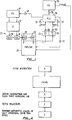
- Fig. 1 is a high-level block diagram of a preferred embodiment.
- a fetch unit (FU) 10 is coupled to an instruction cache (IC) 12.
- the Fin 12 includes address calculation hardware controlled by an address state machine that increments addresses during normal sequential operation and calculates branch target (BRANCH-TARG) addresses for conditional branch and jump instructions.
- the output of the IC 12 is coupled to instruction queue registers (IQR) 14 and 16.
- IQRs 14 and 16 and first and second rank O pipeline registers (ROS and ROF) 18 and 20 are connected in series to form an instruction queue 21.
- the outputs of ROS and ROF 18 and 20 are coupled, respectively, to the inputs of first and second rank 1 registers and to the inputs of a second decode unit and a first decode unit (DCS and DCF) 22 and 24.
- DCS and DCF first decode unit
- the output of the two decode units 22 and 24 are connected to the data inputs of a pairing logic unit (PLU) 26 by first and second DCO buses 28 and 30. Status bits on these buses are connected to control inputs of the PLU 26 by first and second status buses 32 and 34.
- the PLU 16 includes a data output coupled to an execution unit (EU) 36 by a merged decode bus (MDB) 38, an FU control output coupled to the FU 26 by an FUC bus 40, and a PU control output coupled to the PU 25 by a PUC bus 42.
- EU 36 also assert the below described FIssue signal.
- the operation of the system of Fig. 1 will now be described.
- the first and second instructions in the family of instructions are stored in ROF and ROS 20 and 18, respectively. These instructions are decoded at the respective decode units 22 and 24 and the decode results are output on the respective DCO buses 28 and 30.
- the first decode result includes a first entry point field (EPT-F) and a first set of status bits and the second decode result includes a second entry point field (EPT-S) and a second set of status bits.
- the status bits in each decode result indicate whether the respective instruction is a PC and what resources are required to execute the instruction.
- the status information from both decode results is routed to the PLU control ports on the status buses 32 and 34.
- a first status bit is designated PC and indicates whether the instruction is a pair candidate.
- a second status bit is designated EPTIssue and indicates whether the macro instruction requires only clock or requires multiple clocks. If so, then the following instruction may he issued during the next clock. If not, then the data in ROE and ROS 20 and 18 doesn't change until an FI issue occurs. This signal is received by the FU 10 to restart prefetching.
- Other status bits indicate whether the instruction requires the ALU or memory addressing logic to execute.
- the output of the PLU 26 depends on the status information and will be one of three possibilities. First, if the first instruction is not a PC the decode result of the first instruction is output on the MDB 38 to access the microcode routine for singly executing the first instruction. Additionally, the signals issued on the FUC line 40 and the PUC line 42 cause a next single instruction to be fetched from the IC 12 and only the first instruction (stored in ROF 20) to be issued to the next stage of the PU 25. Thus, the concurrent issuing capability of the processor is not used.
- the decode results of the first and second instructions are merged and output on the MDB 38.
- the merged decode results access microcode for executing the first and second instructions as a pair.
- the signals issued on the FUC line 40 and the PUC line 42 cause the next two instructions in the program to be fetched from the IC 12 and the pair of instructions stored in the Rank O registers 18 and 20 to be issued to the next stage of Pin 25.
- the first instruction is a PC
- the first and second instructions are not pairable, e.g., because of a resource conflict
- a subfield of the decode result of the first instruction is output on the MDB 38 to access a microcode routine for singly executing the first instruction.
- the signals issued on the FUC line 40 and the PUC line 42 cause a next single instruction to be fetched from the IC 12 and only the first instruction to be issued from the ROF register 20 to the next stage of the PU 25.
- the concurrent issuing capability of the processor is not used.
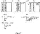
- the operation of the system is best understood by considering concrete examples. These examples are for a processor that utilizes a stack as the data source and data sink for ALU operations. Data is transferred between memory and the stack by load and store operations.
- the stack includes eight physical registers (R0-R7) and a register pointer (RP) which points to the physical register logically assigned to the top of the stack.
- the stack registers are given logic designations A-H, defined by the value of RP, with the register at the top of the stack designated A.
- data dependencies are characterized by stack register conflicts. Another type of dependency is an RP conflict. Instructions generally increment or decrement RP. Thus, a family of instructions may have conflicting requirements for the change of RP.
- Figs. 2 and 3 are schematic diagrams depicting the stack configurations resulting during the execution of a family of two instructions in a standard manner and listing a routine for concurrently executing the instructions according to the present invention.
- FIG. 2 the stack configurations for the sequential single execution of an LDI-LOAD family of two instructions are depicted. Both of these instructions write data to the H register defined relative to the RP.
- immediate data is written to H (R0) and RP is incremented to change H to R1.
- cache data is written to H and RP is incremented again to change H to R2.
- each of these instructions writes data to the H register and increments RP during the R3 pipeline stage.
- concurrent execution would not be possible without special resources and techniques to obviate the effects of these register and RP conflicts.
- the concurrent execution of the pair is described in terms of the relatively deep six stage pipeline, utilized in the preferred embodiment, depicted in Fig. 5.
- the data cache address for the load instruction is generated during Rank 2
- the operands are fetched
- cache data is written to G (R1)
- immediate data is written to H (R0) during Rank 3
- RP is increased by 2 to define R1 as A and R2 as H during Rank 4.
- FIG. 3 the stack configurations for the sequential single execution of an LDD-DADD family of two instructions are depicted.
- RP is incremented to define A as R2
- the high field of OP-2 data is written to A (R2)
- the low field of OP-2 data is written to H (R3) during Rank 2.
- RP is incremented again to define A as R3 during Rank 3.
- OP-2 data is read from the data cache during Rank 3, summed with the contents of registers A (R1) and B (R0) during Rank 4, and the sum written to A (R1) and B (R0) as well as the original OP-2 data written to H (R2) and G (R3) during Rank 5.
- no unresolvable register or RP conflicts occur.
- Fig. 6 depicts a register configuration facilitating the required access.
- a register file 60 includes four write ports and four read ports to allow concurrent transfer of double words.
- bypass circuitry 62, bypass buses 64, wide muxes and cross connections between cache data, immediate data, and the ALU input buses and SBus allow direct access to data prior to its being written to the register file 60.
- the deep pipeline and multiported register file allow microcode to execute many combinations of instructions as families.
- the cache data is transferred directly, during Rank 3, from the data cache to the CDHi and CDLo registers prior to being written to the register file while OP-1 H is transferred from RegA to KHReg and OP-1 L is transferred from RegB to KLReg.
- the sum of transferred data is calculated by the ALU during Rank 4 and written to RegA and Reg B during Rank 5.
- the data in CDHi and CDLo is written to RegH and RegG during Rank 5.
- a family including a load and load immediate instruction can be issued during one clock and processed.
- a family including a load and an add instruction can be issued during one clock and processed.
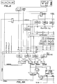
- Fig. 7 is a detailed block diagram illustrating the architecture of an embodiment of the invention.
- the decode units are entry point tables (EPTs) 22 and 24 that respond to the instructions in ROF and ROS 20 and 18 to generate first and second entry points EPF and EPS.
- EPTs entry point tables
- the output of the EPTs 23 and 24 are coupled, respectively, to the first and second DCO buses 28 and 30.
- the first EP bit field F ⁇ 0:15 ⁇ is transferred from EPTF 23 to the first DCO bus 28 and the second EP bit field S ⁇ 4:15 ⁇ is transferred from EPTS 24 to the second DCO bus 30.
- the bit field F ⁇ 1,2,14,15 ⁇ is transferred to the Pairing Logic 72 by the first status bus 32 and the bit field S ⁇ 5,6,7,8 ⁇ is transferred by the second status bus 34.
- bit field F ⁇ 9:15 ⁇ is transferred to the 0 input of a MUX/LOGIC UNIT (MLU) 74 by an FLSB bus 76 and the bit field S ⁇ 9:15 ⁇ is transferred to the 1 input of the MLU 74 by an SLSB bus 78.
- MLU MUX/LOGIC UNIT
- the bit field F ⁇ 2:8 ⁇ is transmitted on an MMSB bus 80 and the output of the MLU 74 is transferred to an MLSB bus 82.
- the MMSB and MLSB buses 80 and 82 are merged to form MSB and LSB sections of the merged EPT (MEPT) bus 38.
- the MFPT is used to access microcode from a microstore 39.
- the Pairing Logic generates PC and EPTIssue signals, transferred on FUC bus 40, that direct the pipeline to issue an instruction pair or a single instruction. Additionally, a NonPaired PC signal is transmitted on an PCNP line 84 coupled to the 09 input of the MLU 74 and the bit F ⁇ 2 ⁇ is transmitted on a mux control line 86 to the control input of the MLU 74.
- Fig. 8 is a memory map of the microstore 39 addressed by MEPT ⁇ 2:15 ⁇ .
- the MSB field of the MEPT is always equal to F ⁇ 2:8 ⁇ where F ⁇ 2 ⁇ is the MSB.
- the LSB field of the MEPT is equal to the output of MLU 74 and depends on the signals on the NPPC and mux control lines 84 and 86.
- the MSB, F ⁇ 2 ⁇ , of all PCs has a value of 1 and for all non-PCs has a value of 0.
- the MSB For a first instruction that is not a pair candidate the MSB, F ⁇ 2 ⁇ , is 0 and the microcode address (MEPT) is located in the lower half 90 of the address space 92. For a first instruction that is a pair candidate the MSB, F ⁇ 2 ⁇ , is 1 and the microcode address (MEPT) is the upper half 94 of the address space.
- the MEPT accesses microcode for executing the first instruction as a single.
- the address of the microcode for executing a non-paired pair candidate is located in the upper half 94 of the address space 92 depicted in Fig. 8.
- events such an exception or branch misprediction, may occur that prevent the successful execution and retirement of the issued instruction pair.
- events such an exception or branch misprediction.
- the following is a description of unique exception handling and branching techniques for efficiently coping with the occurrence of these events.
- an exception is caused by a condition internal to the processor that prevents the execution of an instruction.
- Examples of such conditions include arithmetic overflows for ALU type instructions and page faults for memory reference type of instructions.
- the present solution utilizes the exception handling procedures already existing for handling exceptions for singly issued instructions.
- the microcode for implementing the pair detects an exception by testing for the presence of an exception condition during rank 4 of the pipeline. This procedure is depicted in the flow chart of Fig. 9. If an exception is detected then the unpaired restart procedure is called to abort the instruction pair and reissue the first instruction in the pair singly.
- This consistent macrostate is presented by an unpaired restart procedure, depicted in the flow chart of Fig. 10, that includes the step of inhibiting the loads and stores that occur during rank 5 if an exception is detected in rank 4.
- the contents of the stack registers are not changed and the internal macrostate is the state resulting from the execution of the instruction in the program that immediately precedes the aborted pair.
- This macrostate is consistent with the state that would be presented to the exception handling procedures if the program were executed by a non-paired instruction machine.
- the unpaired restart flushes the pipeline and reissues the first instruction of the pair as a single. If the exception was associated with the first instruction, then the singles microcode will again encounter the same exception and can handle the exception as in a non-paired instruction machine.
- the first instruction will complete without incident and the second instruction will again encounter the exception. If the second instruction is not paired this time then the singles microcode will handle the exception. If it is paired then another unpaired restart will occur.
- Figs. 11A through 11G depict the various pipeline stages and procedures for handling an exception while a pair of instructions is executing.
- the pipeline 25 is divided into instruction and address sides that include instruction and address queues 21I and 21A and instruction and address rank register sets 25I and 25A. Additionally, an instruction mux 90I and an address mux 90A selectively couple the outputs of the IQ2 and IQ3 registers and rank 5 registers of the instruction and address sides, respectively, to the address calculation hardware of the Fin 10.
- Figs. 11B through 11G buses and registers that are enabled are indicated by bold lines.
- the instruction pair A + B is ready to issue and is output from the rank 0 registers 18I and 20I of the instruction side and the addresses of A and B from the rank 0 registers 18A and 20A on the address side.
- the bits of the instructions are transferred to the EPTs on DCO buses 28 and 30.
- Figs. 11C through 11F depict the progress of the instruction pair from rank 1 to rank 4.
- the microcode tests for an exception such as the setting of an arithmetic overflow bit or a page fault. If no exception is detected the pair continues through rank 5 and is retired.
- This testing may be implemented by a conditional branch in the microcode that utilizes an exception status bit as a branch condition bit.
- an exception indicating bit could be the arithmetic overflow bit stored in a condition code register.
- Fig. 11G illustrates the unpaired restart procedure.
- the microcode controls the address mux 90A to transfer the address of instruction A to the address calculation hardware. Additionally, the pair A + B and their addresses are loaded into the rank 1 through 5 registers of the instruction and address sides respectively to begin the flush of the pipeline.
- the instruction calculating hardware accesses the instruction A from the IC 12 and the microcode controls the IQ muxes to route the instruction to the instruction R0 registers 20I and the instruction address to address R0 register 20A.
- instruction A and its address have been transferred to the instruction ROF and the address ROF 20I and 20A, respectively.
- Fig. 11K is a block diagram of a control system for implementing the unpaired restart procedure.
- the output of the control store is coupled to an MCR3 register 100 which, in addition to MCR4 and MCR5 registers 102 and 104, form a microcode pipeline which operates in synchronism with the instruction pipeline 25 to provide required control signals to execute the instruction families in the pipeline.
- the rank 4 microcode includes an m-bit field which is coupled to the first input port of an AND gate 106.
- An exception indication test bit field generated by ALU 108 of the EU 36 is coupled to the input of a latched MUX 110.
- the control port of MUX 110 is coupled to a control field of the rank 5 microcode and the output is coupled to the second input port of the AND gate 106.
- the output of the AND gate 106 is coupled to the input of a first decoder (DEC1) 112.
- DEC1 first decoder
- the outputs of DEC1 are the control signals which cause the pipeline to be flushed and the Rank 5 write operations to be inhibited in the event that an exception condition is detected.
- the control field of rank 5 microcode causes the MUX 110 to transmit the particular exception indication test bit to be tested for the instruction family being executed. If an exception condition has occurred then the transmitted test bit is a logical "1", AND gate 106 is open, and the m-bit Rank 4 microcode field is decoded to generate the control signals for implementing the unpaired restart procedure. If the exception condition has not occurred then the transmitted test bit is a logical "0", the AND gate 106 is closed, and the outputs of the decoder do not cause the unpaired restart procedure to be implemented.
- a branch prediction ram (BPR) is included.
- BPB branch prediction bit
- Fig. 12 if the BPB predicts that the branch will not be taken then prefetching continues in order of ascending addresses. If the branch is predicted taken, then prefetching stops while the address of the target address is formed. Once this target address is formed, prefetching resumes at the target location.
- the MEPT is uniquely determined by the bits of the first and second instructions in a pair and reflects the order of the instructions, i.e., the MSB field includes bits from the EP of the first instruction and the LSB field includes bits from the EP of the second instruction.
- This unique MEPT accesses microcode that includes an indication of whether the first or second instruction is the branch instruction.
- the branch condition is evaluated at rank 4.
- the BPB moves through the pipeline as a PipeID bit along with the pair or instructions and is compared to the branch condition bit (BCB) set by a previously executed instruction. If the BPB and branch condition bit match, then the contents of the pipeline are correct, normal processing continues, and the instruction pair is retired. If the BPB and BCB do not match, then the following instructions in the pipeline are incorrect and branch recovery must occur.
- BCB branch condition bit
- the first step in branch recovery depends on whether the branch instruction is the first or second instruction in the pair. As described above, the microcode routine is different for the two cases. If the mispredicted branch instruction is the first instruction of the pair, then the rank 5 stores of the second instruction must be inhibited because that instruction is not the instruction that is to be executed subsequent to the first instruction. Additionally, all subsequent instructions are flushed from the pipeline and any updates required for the branch are redone.
- mispredicted branch instruction is the second instruction of the pair
- the Rank 5 stores associated with the instruction pair are completed. The remaining stages of the pipeline and the prefetch queue are flushed as before.
- Branch is First/Second Branch was Predicted Taken? Next Address First Yes R5PF + 1 First No TARG of R5PF Second Yes R5PS + 1 Second No TARG of R5PS
- Address recalculation is required only when the BPB does not match the BCB. Since the branch prediction was incorrect the instructions in the pipeline following the branch instruction are incorrect. Thus, if the BPB indicates that the branch is taken then the address of the instruction in the pipeline following the branch instruction is BRANCH-TARG. However, the following instruction address should be BRANCH + 1. Similarly, if the BPB indicates that the branch is not taken then the address of the instruction in the pipeline following the branch instruction is BRANCH + 1. However, the following instruction address should be BRANCH-TARG.
- the microcode indicates that the first instruction in the pair, now resident in register R5I-F of the pipeline, is the branch instruction. Since the BPB mispredicted that the branch would be taken, the address of the next instruction should be BRANCH + 1 instead of BRANCH-TARG.
- the address of the branch instruction, now resident in register R5P-F, is transferred to the address calculation hardware of the FU 10 via the address side MUX 90A. This address incremented to form the address, BRANCH + 1, of the next instruction to be fetched.
- the microcode indicates that the first instruction is the branch instruction. Since the BPB mispredicted that the branch would not be taken, the address of the next instruction should be BRANCH-TARG instead of BRANCH + 1.
- the branch instruction and its address, now resident in registers R5I-F and R5P-F, respectively, are routed to the address calculation hardware of the FU 10 via the instruction side and address side MUXes 90I and 90B.
- the address calculation hardware then calculates the address, BRANCH-TARG, of the next instruction to be fetched.
- Fig. 14 is a block diagram of a control system for implementing the branch prediction mechanism.
- the control store 39 and MCR3, MCR4, and MCR5 registers 100, 102, and 104 are coupled as described above with reference to Fig. 11K.
- each rank of the control pipeline includes a Pipe ID (PID) register 120 which stores certain information regarding the instruction being executed.
- a branch prediction RAM (BPR) 122 has an output coupled to the PID register 120 so that a branch prediction bit (BPB) is propogated through the pipeline for a branch instruction being executed.
- BPR branch prediction RAM
- the BPB stored in the Rank 4 PID register 120 is coupled to a first input of a comparator 124 and a branch condition bit stored in a condition code register 126 or transferred from the ALU is coupled to the second input of the comparator 124.
- An n-bit field of the Rank 4 microcode is coupled to the first input and the output of the comparator 124 is coupled to the second input of an AND gate 128 via MUX 127.
- MUX 127 is controlled by a control field of the Rank 4 microcode.
- the output of the AND gate 128 is coupled to the input of a decoder (DECA) 130.
- the outputs of DECA 130 are the control signals which cause the branch prediction mechanism to be implemented.
- the operation of the system depicted in Fig. 14 will now be described for four separate cases.
- the first two cases relate to conditional branch instructions where the BCB is a bit set in the condition code register 126 by a previously executed instruction.
- the two cases are distinguished by whether the previous instruction was included in a previously executed family or in the current family that includes the branch instruction.
- the second two cases relate to a conditional branch instruction where the BCB is calculated by the ALU using data stored in the register file, for example RegA, by a previously executed instruction. Again the two cases are distinguished by whether the previous instruction is included in the current family.
- the BCB in the condition code register 126 has been set during the execution of a previous instruction. If the BCB and the BPB from the PID 120 register do not match then the branch was mispredicted and the output of the comparator 124 opens AND gate 128.
- the n-bit Rank 4 microcode field is then passed to DECA 130 to generate the control signals required to implement the branch prediction mechanism. As described above, the n-bit field indicates the position of the branch instruction in the family and thus the output of the decoder will differ depending on this location.
- the BCB is a bit from the condition code register 126 that is being written by an instruction in the current family then the BCB bit must be provided to the comparator 124 prior to being written to the register file.
- the MUX 127 is controlled to provide the output of the ALU directly to the comparator 124 during Rank 4 and then the BCB is written to the condition code register during Rank 4.
- the register data is transferred to the ALU and the ALU output is transferred to the comparator 124 via the MUX 127.
- the register data is generated by an instruction in the current family, the data is provided to the ALU, utilizing the hardware described with reference to Fig. 6, prior to being written to the register file and the ALU output is transferred to the comparator 124 via the MUX 127 during Rank 4. The data is then written to the register file during Rank 5.
- the invention has been described for a system for concurrently executing families of two instructions, however the principles of the invention are equally applicable to families of more than two instructions.
- the pairing logic would be modified to respond to more than two status fields and special microcode routines would be written to concurrently execute the family.
- microcoded processor has been described the system is applicable to machines using logic arrays to generate control signals. Both systems have advantages in certain situations and the choice is not critical to practicing the invention. Further, a register configuration other than a register stack can be utilized.
- the status bits described with reference to Fig. 7 are used by the pairing logic to determine whether to merge the EPs of the family of instructions. Alternatively, the EPs could always be merged and the accessed microcode would control whether the family of instructions is issued concurrently.
- Microcode routines can be provided for every possible pair of instructions from the target instruction set.
Applications Claiming Priority (3)
| Application Number | Priority Date | Filing Date | Title |
|---|---|---|---|
| US07/356,316 US5072364A (en) | 1989-05-24 | 1989-05-24 | Method and apparatus for recovering from an incorrect branch prediction in a processor that executes a family of instructions in parallel |
| US356316 | 1989-05-25 | ||
| EP90305487A EP0399760B1 (de) | 1989-05-24 | 1990-05-21 | Mechanismus zur Verzweigungsrücksetzung in einem Prozessor mit gepaarten Befehlen |
Related Parent Applications (1)
| Application Number | Title | Priority Date | Filing Date |
|---|---|---|---|
| EP90305487A Division EP0399760B1 (de) | 1989-05-24 | 1990-05-21 | Mechanismus zur Verzweigungsrücksetzung in einem Prozessor mit gepaarten Befehlen |
Publications (2)
| Publication Number | Publication Date |
|---|---|
| EP0939364A2 true EP0939364A2 (de) | 1999-09-01 |
| EP0939364A3 EP0939364A3 (de) | 2001-06-27 |
Family
ID=23400969
Family Applications (2)
| Application Number | Title | Priority Date | Filing Date |
|---|---|---|---|
| EP90305487A Expired - Lifetime EP0399760B1 (de) | 1989-05-24 | 1990-05-21 | Mechanismus zur Verzweigungsrücksetzung in einem Prozessor mit gepaarten Befehlen |
| EP99101709A Withdrawn EP0939364A3 (de) | 1989-05-24 | 1990-05-21 | Mechanismus zur Verzweigungsrücksetzung in einem Prozessor mit gepaarten Befehlen |
Family Applications Before (1)
| Application Number | Title | Priority Date | Filing Date |
|---|---|---|---|
| EP90305487A Expired - Lifetime EP0399760B1 (de) | 1989-05-24 | 1990-05-21 | Mechanismus zur Verzweigungsrücksetzung in einem Prozessor mit gepaarten Befehlen |
Country Status (6)
| Country | Link |
|---|---|
| US (1) | US5072364A (de) |
| EP (2) | EP0399760B1 (de) |
| JP (1) | JP2846406B2 (de) |
| AU (1) | AU631874B2 (de) |
| CA (1) | CA2016254A1 (de) |
| DE (1) | DE69033443T2 (de) |
Families Citing this family (47)
| Publication number | Priority date | Publication date | Assignee | Title |
|---|---|---|---|---|
| JP2810068B2 (ja) * | 1988-11-11 | 1998-10-15 | 株式会社日立製作所 | プロセッサシステム、コンピュータシステム及び命令処理方法 |
| CA2016068C (en) * | 1989-05-24 | 2000-04-04 | Robert W. Horst | Multiple instruction issue computer architecture |
| EP0404068A3 (de) * | 1989-06-20 | 1991-12-27 | Fujitsu Limited | Vorrichtung zur Ausführung eines Verzweigungsbefehls |
| US5487156A (en) * | 1989-12-15 | 1996-01-23 | Popescu; Valeri | Processor architecture having independently fetching issuing and updating operations of instructions which are sequentially assigned and stored in order fetched |
| US5185871A (en) * | 1989-12-26 | 1993-02-09 | International Business Machines Corporation | Coordination of out-of-sequence fetching between multiple processors using re-execution of instructions |
| US5230068A (en) * | 1990-02-26 | 1993-07-20 | Nexgen Microsystems | Cache memory system for dynamically altering single cache memory line as either branch target entry or pre-fetch instruction queue based upon instruction sequence |
| US5226130A (en) * | 1990-02-26 | 1993-07-06 | Nexgen Microsystems | Method and apparatus for store-into-instruction-stream detection and maintaining branch prediction cache consistency |
| JP2834292B2 (ja) * | 1990-08-15 | 1998-12-09 | 株式会社日立製作所 | データ・プロセッサ |
| US5442772A (en) * | 1991-03-29 | 1995-08-15 | International Business Machines Corporation | Common breakpoint in virtual time logic simulation for parallel processors |
| US5630157A (en) * | 1991-06-13 | 1997-05-13 | International Business Machines Corporation | Computer organization for multiple and out-of-order execution of condition code testing and setting instructions |
| US5493687A (en) | 1991-07-08 | 1996-02-20 | Seiko Epson Corporation | RISC microprocessor architecture implementing multiple typed register sets |
| US5826055A (en) * | 1991-07-08 | 1998-10-20 | Seiko Epson Corporation | System and method for retiring instructions in a superscalar microprocessor |
| US5539911A (en) | 1991-07-08 | 1996-07-23 | Seiko Epson Corporation | High-performance, superscalar-based computer system with out-of-order instruction execution |
| DE4237417C2 (de) * | 1992-03-25 | 1997-01-30 | Hewlett Packard Co | Datenverarbeitungssystem |
| EP0636256B1 (de) | 1992-03-31 | 1997-06-04 | Seiko Epson Corporation | Befehlsablauffolgeplanung von einem risc-superskalarprozessor |
| DE69308548T2 (de) * | 1992-05-01 | 1997-06-12 | Seiko Epson Corp | Vorrichtung und verfahren zum befehlsabschluss in einem superskalaren prozessor. |
| JP2922723B2 (ja) * | 1992-06-29 | 1999-07-26 | キヤノン株式会社 | 情報処理装置 |
| CA2105806C (en) * | 1992-09-18 | 2001-11-20 | Paul V. Jeffs | Apparatus for implementing interrupts in pipelined processors |
| US5617549A (en) * | 1992-10-06 | 1997-04-01 | Hewlett-Packard Co | System and method for selecting and buffering even and odd instructions for simultaneous execution in a computer |
| DE69330889T2 (de) | 1992-12-31 | 2002-03-28 | Seiko Epson Corp | System und Verfahren zur Änderung der Namen von Registern |
| US5628021A (en) | 1992-12-31 | 1997-05-06 | Seiko Epson Corporation | System and method for assigning tags to control instruction processing in a superscalar processor |
| US6032244A (en) * | 1993-01-04 | 2000-02-29 | Cornell Research Foundation, Inc. | Multiple issue static speculative instruction scheduling with path tag and precise interrupt handling |
| US5748976A (en) * | 1993-10-18 | 1998-05-05 | Amdahl Corporation | Mechanism for maintaining data coherency in a branch history instruction cache |
| WO1995016952A1 (en) * | 1993-12-15 | 1995-06-22 | Silicon Graphics Inc. | Superscalar microprocessor instruction pipeline including instruction dispatch and release control |
| SG52391A1 (en) * | 1994-01-03 | 1998-09-28 | Intel Corp | Method and apparatus for implementing a four stage branch resolution system in a computer processor |
| US5809271A (en) * | 1994-03-01 | 1998-09-15 | Intel Corporation | Method and apparatus for changing flow of control in a processor |
| US5644779A (en) * | 1994-04-15 | 1997-07-01 | International Business Machines Corporation | Processing system and method of operation for concurrent processing of branch instructions with cancelling of processing of a branch instruction |
| US5623694A (en) * | 1994-10-03 | 1997-04-22 | International Business Machines Corporation | Aborting an I/O operation started before all system data is received by the I/O controller after detecting a remote retry operation |
| US5625808A (en) * | 1995-03-31 | 1997-04-29 | International Business Machines Corporation | Read only store as part of cache store for storing frequently used millicode instructions |
| US5634103A (en) * | 1995-11-09 | 1997-05-27 | International Business Machines Corporation | Method and system for minimizing branch misprediction penalties within a processor |
| JPH09319569A (ja) * | 1996-05-31 | 1997-12-12 | Mitsubishi Electric Corp | マイクロコンピュータ |
| KR100445054B1 (ko) * | 1996-06-29 | 2004-11-02 | 주식회사 하이닉스반도체 | 마이크로프로세서의브랜치처리를위한방법 |
| US6088793A (en) * | 1996-12-30 | 2000-07-11 | Intel Corporation | Method and apparatus for branch execution on a multiple-instruction-set-architecture microprocessor |
| US5974538A (en) * | 1997-02-21 | 1999-10-26 | Wilmot, Ii; Richard Byron | Method and apparatus for annotating operands in a computer system with source instruction identifiers |
| US6150724A (en) * | 1998-03-02 | 2000-11-21 | Motorola, Inc. | Multi-chip semiconductor device and method for making the device by using multiple flip chip interfaces |
| US6055630A (en) * | 1998-04-20 | 2000-04-25 | Intel Corporation | System and method for processing a plurality of branch instructions by a plurality of storage devices and pipeline units |
| SE9901145D0 (sv) | 1998-11-16 | 1999-03-29 | Ericsson Telefon Ab L M | A processing system and method |
| EP1131703A1 (de) * | 1998-11-16 | 2001-09-12 | Telefonaktiebolaget Lm Ericsson | Simultanes verarbeitungssystem für veranstaltungsbasierte systeme |
| SE9901146D0 (sv) * | 1998-11-16 | 1999-03-29 | Ericsson Telefon Ab L M | A processing system and method |
| SE9803901D0 (sv) * | 1998-11-16 | 1998-11-16 | Ericsson Telefon Ab L M | a device for a service network |
| GB2355084B (en) * | 1999-07-21 | 2004-04-28 | Element 14 Ltd | Setting condition values in a computer |
| US6636960B1 (en) * | 2000-02-16 | 2003-10-21 | Hewlett-Packard Development Company, L.P. | Method and apparatus for resteering failing speculation check instructions |
| GB2403833B (en) * | 2000-02-16 | 2005-02-23 | Hewlett Packard Co | Method and apparatus for resteering failing speculation check instructions field |
| DE10101949C1 (de) * | 2001-01-17 | 2002-08-08 | Infineon Technologies Ag | Datenverarbeitungsverfahren |
| US7747843B2 (en) * | 2004-06-02 | 2010-06-29 | Broadcom Corporation | Microprocessor with integrated high speed memory |
| US7216218B2 (en) * | 2004-06-02 | 2007-05-08 | Broadcom Corporation | Microprocessor with high speed memory integrated in load/store unit to efficiently perform scatter and gather operations |
| US11144364B2 (en) | 2019-01-25 | 2021-10-12 | International Business Machines Corporation | Supporting speculative microprocessor instruction execution |
Citations (3)
| Publication number | Priority date | Publication date | Assignee | Title |
|---|---|---|---|---|
| EP0239081A2 (de) * | 1986-03-26 | 1987-09-30 | Hitachi, Ltd. | Datenprozessor in Pipelinestruktur mit der Fähigkeit mehrere Befehle parallel zu dekodieren und auszuführen |
| US4760520A (en) * | 1984-10-31 | 1988-07-26 | Hitachi, Ltd. | Data processor capable of executing instructions under prediction |
| EP0354740A2 (de) * | 1988-08-09 | 1990-02-14 | Matsushita Electric Industrial Co., Ltd. | Datenverarbeitungsgerät zur parallelen Dekodierung und parallelen Ausführung von Befehlen mit variabler Wortlänge |
Family Cites Families (4)
| Publication number | Priority date | Publication date | Assignee | Title |
|---|---|---|---|---|
| US4398243A (en) * | 1980-04-25 | 1983-08-09 | Data General Corporation | Data processing system having a unique instruction processor system |
| WO1985000453A1 (en) * | 1983-07-11 | 1985-01-31 | Prime Computer, Inc. | Data processing system |
| US4685058A (en) * | 1983-08-29 | 1987-08-04 | Amdahl Corporation | Two-stage pipelined execution unit and control stores |
| US4777587A (en) * | 1985-08-30 | 1988-10-11 | Advanced Micro Devices, Inc. | System for processing single-cycle branch instruction in a pipeline having relative, absolute, indirect and trap addresses |
-
1989
- 1989-05-24 US US07/356,316 patent/US5072364A/en not_active Expired - Lifetime
-
1990
- 1990-05-08 CA CA002016254A patent/CA2016254A1/en not_active Abandoned
- 1990-05-15 AU AU55047/90A patent/AU631874B2/en not_active Ceased
- 1990-05-21 EP EP90305487A patent/EP0399760B1/de not_active Expired - Lifetime
- 1990-05-21 EP EP99101709A patent/EP0939364A3/de not_active Withdrawn
- 1990-05-21 DE DE69033443T patent/DE69033443T2/de not_active Expired - Lifetime
- 1990-05-22 JP JP2132425A patent/JP2846406B2/ja not_active Expired - Lifetime
Patent Citations (3)
| Publication number | Priority date | Publication date | Assignee | Title |
|---|---|---|---|---|
| US4760520A (en) * | 1984-10-31 | 1988-07-26 | Hitachi, Ltd. | Data processor capable of executing instructions under prediction |
| EP0239081A2 (de) * | 1986-03-26 | 1987-09-30 | Hitachi, Ltd. | Datenprozessor in Pipelinestruktur mit der Fähigkeit mehrere Befehle parallel zu dekodieren und auszuführen |
| EP0354740A2 (de) * | 1988-08-09 | 1990-02-14 | Matsushita Electric Industrial Co., Ltd. | Datenverarbeitungsgerät zur parallelen Dekodierung und parallelen Ausführung von Befehlen mit variabler Wortlänge |
Non-Patent Citations (2)
| Title |
|---|
| "COMPREHENSIVE BRANCH PREDICTION MECHANISM FOR BC" IBM TECHNICAL DISCLOSURE BULLETIN,US,IBM CORP. NEW YORK, vol. 28, no. 5, 1 October 1985 (1985-10-01), pages 2255-2262, XP002035564 ISSN: 0018-8689 * |
| L. C. GARCIA ET AL.: "Storage Access-Exception Detection for Pipelined Execution Units" IBM TECHNICAL DISCLOSURE BULLETIN., vol. 25, no. 12, May 1983 (1983-05), pages 6711-12, XP002165704 IBM CORP. NEW YORK., US ISSN: 0018-8689 * |
Also Published As
| Publication number | Publication date |
|---|---|
| DE69033443D1 (de) | 2000-03-09 |
| DE69033443T2 (de) | 2000-06-29 |
| EP0399760A2 (de) | 1990-11-28 |
| US5072364A (en) | 1991-12-10 |
| AU631874B2 (en) | 1992-12-10 |
| CA2016254A1 (en) | 1990-11-23 |
| JP2846406B2 (ja) | 1999-01-13 |
| AU5504790A (en) | 1990-11-29 |
| EP0399760A3 (de) | 1993-05-19 |
| JPH03116235A (ja) | 1991-05-17 |
| EP0399760B1 (de) | 2000-02-02 |
| EP0939364A3 (de) | 2001-06-27 |
Similar Documents
| Publication | Publication Date | Title |
|---|---|---|
| EP0399760B1 (de) | Mechanismus zur Verzweigungsrücksetzung in einem Prozessor mit gepaarten Befehlen | |
| EP0399762B1 (de) | Rechnerarchitektur mit Mehrfachbefehlsausgabe | |
| EP0399757B1 (de) | Mechanismus zur präzisen Behandlung von Ausnahmebedingungen in einem Prozessor mit gepaarten Befehlen | |
| EP0605872B1 (de) | Verfahren und System für spekulative Befehlsausführung | |
| US6247122B1 (en) | Method and apparatus for performing branch prediction combining static and dynamic branch predictors | |
| EP0751458B1 (de) | Verfahren und Anordnung zur Überwachung von Ressourcenzuteilung innerhalb eines Prozessors | |
| KR100616722B1 (ko) | 수퍼스칼라프로세서내의파이프라인명령디스패치유닛 | |
| US20060236080A1 (en) | Reducing the fetch time of target instructions of a predicted taken branch instruction | |
| US6981131B2 (en) | Early condition code evaluation at pipeline stages generating pass signals for controlling coprocessor pipeline executing same conditional instruction | |
| JPH0785223B2 (ja) | デジタル・コンピュータ及び分岐命令実行方法 | |
| US5898864A (en) | Method and system for executing a context-altering instruction without performing a context-synchronization operation within high-performance processors | |
| EP0378415A2 (de) | Verteilungsmechanismus für mehrere Befehle | |
| EP0778519B1 (de) | System zur Zuteilung mehrerer Befehle ohne Verzweigungsunterbrechung in einem Pipelineprozessor | |
| KR100305487B1 (ko) | 특정유형의인스트럭션을동시에처리할수있는방법및데이터프로세싱시스템 | |
| US6421774B1 (en) | Static branch predictor using opcode of instruction preceding conditional branch | |
| US5850563A (en) | Processor and method for out-of-order completion of floating-point operations during load/store multiple operations | |
| US6044460A (en) | System and method for PC-relative address generation in a microprocessor with a pipeline architecture | |
| US6718460B1 (en) | Mechanism for error handling in a computer system |
Legal Events
| Date | Code | Title | Description |
|---|---|---|---|
| PUAI | Public reference made under article 153(3) epc to a published international application that has entered the european phase |
Free format text: ORIGINAL CODE: 0009012 |
|
| AC | Divisional application: reference to earlier application |
Ref document number: 399760 Country of ref document: EP |
|
| AK | Designated contracting states |
Kind code of ref document: A2 Designated state(s): DE FR GB IT SE |
|
| RAP1 | Party data changed (applicant data changed or rights of an application transferred) |
Owner name: COMPAQ COMPUTER CORPORATION |
|
| PUAL | Search report despatched |
Free format text: ORIGINAL CODE: 0009013 |
|
| AK | Designated contracting states |
Kind code of ref document: A3 Designated state(s): DE FR GB IT SE |
|
| 17P | Request for examination filed |
Effective date: 20011220 |
|
| RAP1 | Party data changed (applicant data changed or rights of an application transferred) |
Owner name: HEWLETT-PACKARD DEVELOPMENT COMPANY, L.P. |
|
| STAA | Information on the status of an ep patent application or granted ep patent |
Free format text: STATUS: THE APPLICATION IS DEEMED TO BE WITHDRAWN |
|
| 18D | Application deemed to be withdrawn |
Effective date: 20051201 |