EP0936731A1 - Vorwärtsgekoppelter Verstärker - Google Patents
Vorwärtsgekoppelter Verstärker Download PDFInfo
- Publication number
- EP0936731A1 EP0936731A1 EP99102396A EP99102396A EP0936731A1 EP 0936731 A1 EP0936731 A1 EP 0936731A1 EP 99102396 A EP99102396 A EP 99102396A EP 99102396 A EP99102396 A EP 99102396A EP 0936731 A1 EP0936731 A1 EP 0936731A1
- Authority
- EP
- European Patent Office
- Prior art keywords
- power
- amplifier
- distortion
- output signal
- output
- Prior art date
- Legal status (The legal status is an assumption and is not a legal conclusion. Google has not performed a legal analysis and makes no representation as to the accuracy of the status listed.)
- Granted
Links
Images


Classifications
-
- H—ELECTRICITY
- H03—ELECTRONIC CIRCUITRY
- H03F—AMPLIFIERS
- H03F1/00—Details of amplifiers with only discharge tubes, only semiconductor devices or only unspecified devices as amplifying elements
- H03F1/32—Modifications of amplifiers to reduce non-linear distortion
- H03F1/3241—Modifications of amplifiers to reduce non-linear distortion using predistortion circuits
- H03F1/3252—Modifications of amplifiers to reduce non-linear distortion using predistortion circuits using multiple parallel paths between input and output
-
- H—ELECTRICITY
- H03—ELECTRONIC CIRCUITRY
- H03F—AMPLIFIERS
- H03F1/00—Details of amplifiers with only discharge tubes, only semiconductor devices or only unspecified devices as amplifying elements
- H03F1/32—Modifications of amplifiers to reduce non-linear distortion
- H03F1/3223—Modifications of amplifiers to reduce non-linear distortion using feed-forward
Definitions
- the present invention relates to a feed forward amplifier used for a base station for mobile communication equipment.
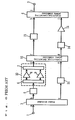
- FIG. 6 shows an example of a configuration of a conventional feed forward amplifier.
- 1 is an input terminal
- 2 is an output terminal
- 3 and 6 are power dividers
- 4 is a distortion canceling power combiner
- 5 and 14 are vector adjusters
- 7 is an output power combiner
- 8 and 9 are power amplifiers
- 11 and 13 are delay circuits
- 12 is a distortion detecting power combiner
- 15 is an auxiliary amplifier.
- the power divider 6, the output power combiner 7, and the power amplifiers 8 and 9 constitute a main amplifier 10.
- references (a) to (j) added to the power divider 3, the distortion canceling power combiner 4, and the distortion detecting power combiner 12 designate ports.
- the power divider 3 divides into two an input signal (see FIG. 7(a)) input from the input terminal 1 and containing multi-channel components.
- One of the divided output signals is transferred via the vector adjuster 5 to the main amplifier 10, which then amplifies this signal.
- the amplified signal is input to the port (d) of the distortion detecting power combiner 12 (see FIG. 7(b)). Due to non-linearity of the main amplifier 10, the input signal (see FIG. 7(b)) contains not only the input signal components but also distortion components resulting from inter-modulation.
- the other divided signal is input to the port (e) of the distortion detecting power combiner 12 through the delay circuit 11.
- a signal output from the port (f) and containing both the input signal components and the distortion components is input to the port (h) of the distortion canceling power combiner 4 via the delay circuit 13.
- the signal with the distortion components output from the port (g) is transferred via the vector adjuster 14 to the auxiliary amplifier 15, which then amplifies this signal.
- the amplified signal is then input to the port (i) of the distortion canceling power combiner 4.
- FIGS. 7(a) to 7(d) show the frequency spectra of the signals at the ports (a), (d), (g), and (j) of FIG. 6.
- the output power of the main amplifier 10 decreases due to losses in the distortion detecting power combiner 12 and delay circuit 13 to reduce the efficiency of the entire feed forward amplifier.
- the first invention of the present invention is a feed forward amplifier comprising:
- the second invention of the present invention is a feed forward amplifier according to the first invention comprising an auxiliary amplifier for amplifying the output signal from said second vector adjuster to output the amplified signal to said distortion canceling power combiner, wherein:
- the third invention of the present invention is a feed forward amplifier comprising:
- the fourth invention of the present invention is a feed forward amplifier according to the third invention comprising an auxiliary amplifier for amplifying the output signal from said second vector adjuster to output the amplified signal to said third power divider, wherein:
- the fifth invention of the present invention is a feed forward amplifier according to any one of the first invention to the fourth invention wherein each type of devices used as said power amplifiers and a type of a device used as said distortion detecting amplifier are the same.
- the sixth invention of the present invention is a feed forward amplifier according to any one of the first invention to the fourth invention wherein said distortion detecting amplifier has a distortion characteristic relative to normalized output power that is substantially the same as the distortion characteristic of any of said power amplifiers relative to normalized output power.
- the seventh invention of the present invention is a feed forward amplifier according to any one of the first invention to the sixth invention wherein substantially all output signals output from said distortion detecting amplifier are output to said distortion canceling power combiner.
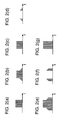
- FIG. 1 is a block diagram of a feed forward amplifier according to Embodiment 1 of this invention.
- 1 is an input terminal
- 2 is an output terminal
- 3, 6, and 22 are power dividers
- 4 is a distortion canceling power combiner
- 7 is an output power combiner
- 8 and 9 are power amplifiers
- 11 and 21 are delay circuits
- 14 and 24 are vector adjusters
- 15 is an auxiliary amplifier
- 23 is a distortion detecting power combiner
- 25 is a distortion detecting power amplifier.
- the power divider 3 is a first power divider
- the delay circuit 21 is a first delay circuit
- the power divider 22 is a second power divider
- the vector adjuster 24 is a first vector adjuster
- the delay circuit 11 is a second delay circuit.
- the power divider 6, the output power combiner 7, and the power amplifiers 8 and 9 constitute a main amplifier 10.
- the power amplifiers 8 and 9 and the distortion detecting amplifier 25 each comprise the same device.
- the power divider 3 divides an input signal 101 into two.
- This input signal 101 is input from the input terminal 1 and containing multi-channel components.
- One of the divided output signals is transferred via the delay circuit 21 to the main amplifier 10, which then amplifies this signal.
- the amplified signal is input to the distortion canceling power combiner 4 (in FIG. 1, reference numeral 105 designates the signal input to the distortion canceling power combiner 4). Due to the non-linearity of the main amplifier 10, the signal 105 contains not only the input signal components but also distortion components resulting from inter-modulation.
- the power divider 22 further divides the other divided signal into two, and one of the output signals is transferred via the vector adjuster 24 to the distortion detecting amplifier 25, which then amplifies this signal (in FIG.
- reference numeral 102 designates the signal amplified by the distortion detecting amplifier 25).
- the signal 102 is output that has the same frequency spectrum as an output signal 105 from the main amplifier 10 (but a different power level, that is, a different amplitude).
- the other output signal divided by the power divider 22 is transferred via the delay circuit 11 to the distortion detecting power combiner 23, which then combines this signal with an output signal from the distortion detecting amplifier 25 (in FIG. 1, reference numeral 103 designates the signal input to the distortion detecting power combiner 23).
- a signal 104 consisting of only the distortion components with the input signal components cancellation is output from the distortion detecting power combiner 23.
- FIGS. 2(a) to 2(g) show the frequency spectra of the signals at each section.
- the signal output from the distortion detecting power combiner 23 and consisting of the distortion components is transferred via the vector adjuster 14 to the auxiliary amplifier 15, which then amplifies this signal.
- the amplified signal is input to the distortion canceling power combiner 4, which then combines this signal with an output signal from the main amplifier 10.
- a signal consisting of only the input signal components with the distortion components cancellation is output from the distortion canceling power combiner 4 to the output terminal 2.
- the configuration in FIG. 1 omits the distortion detecting power combiner otherwise located after the main amplifier and locates the delay circuit before the main amplifier to reduce losses occurring after the main amplifier in order to improve the efficiency of the entire feed forward amplifier.
- Embodiment 1 has been described in conjunction with the example in which the main amplifier is configured by combining the two power amplifiers in parallel, this invention is not limited to this aspect and the main amplifier may be configured using a single power amplifier. In this case, the power divider 6 and the output power combiner 7 may be removed.
- Embodiment 1 has been described in conjunction with the example in which the main amplifier is configured by combining the two power amplifiers in parallel, this invention is not limited to this aspect and the main amplifier may be configured by combining three or more power amplifiers in parallel.
- the power divider 6 may be adapted to divide the input signal into the same number as that of the power amplifiers.
- the distortion detecting amplifier 25 and the power amplifiers 8 and 9 each comprise the same device
- this invention is not limited to this aspect but similar operations can be performed by, for example, configuring the amplifiers in such a way that the distortion characteristic of the distortion detecting amplifier 25 relative to normalized output power (shown in FIG. 3(a)) is the same as the distortion characteristic of one of the power amplifiers 8 and 9 relative to normalized output power (shown in FIG. 3(b)) and that the output power of the distortion detecting amplifier 25 is lower than that of the power amplifiers 8 or 9.
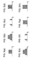
- FIG. 4 is a block diagram of a feed forward amplifier according to Embodiment 2 of this invention.
- 31 is a power divider that is a third power divider and 32 and 33 are distortion canceling power combiners.
- the power divider 6, the output power combiner 7, the power amplifiers 8 and 9, and the distortion canceling power combiners 32 and 33 constitute the main amplifier 10.
- the power amplifiers 8 and 9 and the distortion detecting amplifier 25 each comprise the same device.
- Embodiment 2 of this invention is a feed forward amplifier that cancels the distortion components for each power amplifier of the main amplifier.
- the power divider 3 divides an input signal 301 into two. This input signal 301 is input from the input terminal 1 and containing multi-channel components. One of the divided output signals is transferred via the delay circuit 21 to the power divider 6, which divides this signal into two.
- the power amplifiers 8 and 9 then amplify the divided signals, respectively. Due to the non-linearity of each of the power amplifiers 8 and 9, the output signal contains not only the input signal components but also distortion components resulting from inter-modulation (in FIG. 4, reference numerals 302 and 305 designate the output signals of the power amplifiers 8 and 9, respectively).
- the other signal divided by the power divider 3 is processed as in Embodiment 1, so a signal with only the distortion components amplified is output to the auxiliary amplifier 15.
- the power divider 31 that divides power depending on the number of power amplifiers in the main amplifier 10 divides the output signal from the auxiliary amplifier 15 into two.
- the distortion canceling power combiner 32 combines one output signal 303 of the two output signals divided by the power divider 31, with an output signal 302 from the power amplifier 8.
- the distortion canceling power combiner 33 combines the other output signal 306 with an output signal 305 from the power amplifier 9.
- signals 304 and 307 consisting of only the input signal components with the distortion components cancellation are output from the distortion canceling power combiners 32 and 33, respectively.
- the output power combiner 7 then combines the output signals 304 and 307 from the distortion canceling power combiners 32 and 33 together and outputs to the output terminal 2 a signal 308 consisting of only the input signal components.
- FIGS. 5(a) to 5(h) show the frequency spectra of the signals at each section.
- the configuration in FIG. 4 improves the efficiency of the entire feed forward amplifier as in Embodiment 1.
- Embodiment 2 has been described in conjunction with the example in which the main amplifier is configured by combining the two power amplifiers in parallel, this invention is not limited to this aspect and the main amplifier may be configured by combining three or more power amplifiers in parallel.
- the power divider 6 may be adapted to divide the input signal into the same number as that of the power amplifiers.
- the distortion detecting amplifier 25 and the power amplifiers 8 and 9 each comprise the same device(that is, each type of devices used as said power amplifiers 8 and 9 and the type of the device used as said distortion detecting amplifier 25 are the same ), this invention is not limited to this aspect but similar operations can be performed by, for example, configuring the apparatus in such a way that the distortion characteristic of the distortion detecting amplifier 25 relative to normalized output power is the same as the distortion characteristic of one of the power amplifiers 8 and 9 relative to normalized output power.
- this invention in addition to the plurality of power amplifiers of the main amplifier connected in parallel, this invention includes the amplifier for detecting the distortion components, having a distortion characteristic in a predetermined relationship with the distortion characteristic of the main amplifier.
- This configuration has the advantages of omitting the distortion detecting power combiner otherwise located after the main amplifier and locating the delay circuit before the main amplifier to reduce losses occurring after the main amplifier in order to improve the efficiency of the entire feed forward amplifier.
Landscapes
- Physics & Mathematics (AREA)
- Nonlinear Science (AREA)
- Engineering & Computer Science (AREA)
- Power Engineering (AREA)
- Amplifiers (AREA)
- Transmitters (AREA)
Applications Claiming Priority (2)
| Application Number | Priority Date | Filing Date | Title |
|---|---|---|---|
| JP10027571A JPH11234051A (ja) | 1998-02-09 | 1998-02-09 | フィードフォワード増幅器 |
| JP2757198 | 1998-02-09 |
Publications (2)
| Publication Number | Publication Date |
|---|---|
| EP0936731A1 true EP0936731A1 (de) | 1999-08-18 |
| EP0936731B1 EP0936731B1 (de) | 2006-10-11 |
Family
ID=12224707
Family Applications (1)
| Application Number | Title | Priority Date | Filing Date |
|---|---|---|---|
| EP99102396A Expired - Lifetime EP0936731B1 (de) | 1998-02-09 | 1999-02-08 | Vorwärtsgekoppelter Verstärker |
Country Status (4)
| Country | Link |
|---|---|
| US (1) | US6037837A (de) |
| EP (1) | EP0936731B1 (de) |
| JP (1) | JPH11234051A (de) |
| DE (1) | DE69933492T2 (de) |
Cited By (2)
| Publication number | Priority date | Publication date | Assignee | Title |
|---|---|---|---|---|
| US6239656B1 (en) | 2000-01-31 | 2001-05-29 | Matsushita Electric Industrial Co., Ltd. | Power amplifier |
| EP1241781A1 (de) * | 2001-03-14 | 2002-09-18 | Siemens Aktiengesellschaft | Verfahren und Vorrichtung zur digitalen Vorverzerrungs-/Frequenzgangkompensations- und Feedforward-Linearisierung eines Sendesignals |
Families Citing this family (9)
| Publication number | Priority date | Publication date | Assignee | Title |
|---|---|---|---|---|
| JP2000151295A (ja) * | 1998-11-05 | 2000-05-30 | Mitsubishi Electric Corp | 歪補償回路 |
| US6122492A (en) * | 1999-02-08 | 2000-09-19 | Motorola, Inc. | Adjustable radio frequency power amplifier and transmitter |
| EP1032121A1 (de) * | 1999-02-26 | 2000-08-30 | Koninklijke Philips Electronics N.V. | Elektronisches Gerät mit einem Leistungsverstärker |
| WO2003003569A1 (en) * | 2001-06-29 | 2003-01-09 | Remec, Inc. | Balanced distortion reduction circuit |
| US6420929B1 (en) * | 2001-08-23 | 2002-07-16 | Thomas Ha | N way cancellation coupler for power amplifier |
| US6700442B2 (en) * | 2001-11-20 | 2004-03-02 | Thomas Quang Ha | N way phase cancellation power amplifier |
| JP2003234623A (ja) * | 2002-02-12 | 2003-08-22 | Sharp Corp | 受光アンプ回路及びこれを用いた光ピックアップ |
| US6794933B2 (en) | 2002-02-14 | 2004-09-21 | Powerwave Technologies, Inc. | Fast forward RF power amplifier with high efficiency main amplifier and highly linear error amplifier |
| US8441322B1 (en) | 2011-11-30 | 2013-05-14 | Raytheon Company | Broadband linearization by elimination of harmonics and intermodulation in amplifiers |
Citations (4)
| Publication number | Priority date | Publication date | Assignee | Title |
|---|---|---|---|---|
| US5043673A (en) * | 1989-03-31 | 1991-08-27 | Mitsubishi Denki Kabushiki Kaisha | Compensating circuit for a high frequency amplifier |
| EP0443368A2 (de) * | 1990-02-07 | 1991-08-28 | Fujitsu Limited | Verstärker für kombinierte Wellen mit konstanter Amplitude |
| EP0552059A1 (de) * | 1992-01-16 | 1993-07-21 | Japan Radio Co., Ltd | Leistungsverstärkervorrichtung |
| US5631604A (en) * | 1994-01-11 | 1997-05-20 | Ericsson Inc. | Waste energy control and management in power amplifiers |
Family Cites Families (5)
| Publication number | Priority date | Publication date | Assignee | Title |
|---|---|---|---|---|
| FR2415923A2 (fr) * | 1978-01-25 | 1979-08-24 | Cit Alcatel | Procede de compensation du bruit d'intermodulation et dispositifs pour sa mise en oeuvre |
| JP2697618B2 (ja) * | 1994-07-14 | 1998-01-14 | 日本電気株式会社 | フィードフォワード増幅器 |
| US5644268A (en) * | 1995-01-06 | 1997-07-01 | Spectrian, Inc. | Feed forward RF amplifier for combined signal and error amplification |
| JP3360464B2 (ja) * | 1995-02-13 | 2002-12-24 | 松下電器産業株式会社 | フィードフォワード増幅器 |
| JP3361657B2 (ja) * | 1995-07-20 | 2003-01-07 | 松下電器産業株式会社 | フィードフォワード増幅器の制御装置および制御方法 |
-
1998
- 1998-02-09 JP JP10027571A patent/JPH11234051A/ja not_active Withdrawn
-
1999
- 1999-02-08 EP EP99102396A patent/EP0936731B1/de not_active Expired - Lifetime
- 1999-02-08 DE DE69933492T patent/DE69933492T2/de not_active Expired - Fee Related
- 1999-02-08 US US09/245,681 patent/US6037837A/en not_active Expired - Fee Related
Patent Citations (4)
| Publication number | Priority date | Publication date | Assignee | Title |
|---|---|---|---|---|
| US5043673A (en) * | 1989-03-31 | 1991-08-27 | Mitsubishi Denki Kabushiki Kaisha | Compensating circuit for a high frequency amplifier |
| EP0443368A2 (de) * | 1990-02-07 | 1991-08-28 | Fujitsu Limited | Verstärker für kombinierte Wellen mit konstanter Amplitude |
| EP0552059A1 (de) * | 1992-01-16 | 1993-07-21 | Japan Radio Co., Ltd | Leistungsverstärkervorrichtung |
| US5631604A (en) * | 1994-01-11 | 1997-05-20 | Ericsson Inc. | Waste energy control and management in power amplifiers |
Cited By (3)
| Publication number | Priority date | Publication date | Assignee | Title |
|---|---|---|---|---|
| US6239656B1 (en) | 2000-01-31 | 2001-05-29 | Matsushita Electric Industrial Co., Ltd. | Power amplifier |
| EP1126595A1 (de) * | 2000-01-31 | 2001-08-22 | Matsushita Electric Industrial Co., Ltd. | Leistungsverstärker |
| EP1241781A1 (de) * | 2001-03-14 | 2002-09-18 | Siemens Aktiengesellschaft | Verfahren und Vorrichtung zur digitalen Vorverzerrungs-/Frequenzgangkompensations- und Feedforward-Linearisierung eines Sendesignals |
Also Published As
| Publication number | Publication date |
|---|---|
| DE69933492T2 (de) | 2007-02-01 |
| JPH11234051A (ja) | 1999-08-27 |
| EP0936731B1 (de) | 2006-10-11 |
| DE69933492D1 (de) | 2006-11-23 |
| US6037837A (en) | 2000-03-14 |
Similar Documents
| Publication | Publication Date | Title |
|---|---|---|
| US6326845B1 (en) | Feedforward amplifier | |
| US6646505B2 (en) | Power amplifier array with same type predistortion amplifier | |
| US8965454B2 (en) | Amplifier system for cell sites and other suitable applications | |
| US10483928B2 (en) | Power amplification module | |
| US6037837A (en) | Feed forward amplifier | |
| KR20130123289A (ko) | 초소형 rf 전력증폭기 | |
| US7385541B2 (en) | Power amplifying apparatus, power combining system and delay measuring method for power combining system | |
| US7403070B2 (en) | Band selection type feed forward amplifier | |
| US6720829B2 (en) | Distortion-compensated amplifying circuit | |
| US10187018B2 (en) | Wideband highly linear amplifier | |
| KR100814457B1 (ko) | 이중대역 피드포워드 선형 전력 증폭기 | |
| US6959174B2 (en) | Amplifying device | |
| JP3508646B2 (ja) | 歪み補償増幅器 | |
| KR100371531B1 (ko) | 에러 피드백을 이용한 피드포워드 선형 전력 증폭기 | |
| US6657490B2 (en) | Feedforward signal generation for combined amplifiers | |
| JP2000295048A (ja) | フィードフォワード増幅器 | |
| JPH01302901A (ja) | 多周波同時増幅器における歪補償回路 | |
| EP1289128B1 (de) | Vorwärtsgekoppelter Verstärker und Verfahren zum vorwärtsgekoppelten Verstärken | |
| US7142054B2 (en) | Amplifying signals using a quadrature coupled amplifier | |
| JP2000068754A (ja) | 歪み補償回路 | |
| CN115699565A (zh) | 多赫蒂放大器 | |
| JPH09312526A (ja) | フィードフォワード増幅器 | |
| JP2003258562A (ja) | 歪み補償付き増幅回路 | |
| JP2000236222A (ja) | フィードフォワード増幅器 | |
| KR20010077188A (ko) | 이동 통신 기지국 시스템의 선형 보상 증폭 회로 |
Legal Events
| Date | Code | Title | Description |
|---|---|---|---|
| PUAI | Public reference made under article 153(3) epc to a published international application that has entered the european phase |
Free format text: ORIGINAL CODE: 0009012 |
|
| AK | Designated contracting states |
Kind code of ref document: A1 Designated state(s): DE FR GB |
|
| AX | Request for extension of the european patent |
Free format text: AL;LT;LV;MK;RO;SI |
|
| RIN1 | Information on inventor provided before grant (corrected) |
Inventor name: KUGOU,SHIN'ICHI Inventor name: KOSUGI,HIROAKI Inventor name: ISHIDA,KAORU Inventor name: MIYAJI,MASAYUKI |
|
| RIN1 | Information on inventor provided before grant (corrected) |
Inventor name: KUGOU,SHIN'ICHI Inventor name: KOSUGI,HIROAKI Inventor name: ISHIDA,KAORU Inventor name: MIYAJI,MASAYUKI |
|
| 17P | Request for examination filed |
Effective date: 19991026 |
|
| AKX | Designation fees paid |
Free format text: DE FR GB |
|
| GRAP | Despatch of communication of intention to grant a patent |
Free format text: ORIGINAL CODE: EPIDOSNIGR1 |
|
| RIN1 | Information on inventor provided before grant (corrected) |
Inventor name: KUGOU,SHIN'ICHI Inventor name: KOSUGI,HIROAKI Inventor name: ISHIDA,KAORU Inventor name: MIYAJI,MASAYUKI |
|
| GRAS | Grant fee paid |
Free format text: ORIGINAL CODE: EPIDOSNIGR3 |
|
| GRAA | (expected) grant |
Free format text: ORIGINAL CODE: 0009210 |
|
| AK | Designated contracting states |
Kind code of ref document: B1 Designated state(s): DE FR GB |
|
| REG | Reference to a national code |
Ref country code: GB Ref legal event code: FG4D |
|
| REF | Corresponds to: |
Ref document number: 69933492 Country of ref document: DE Date of ref document: 20061123 Kind code of ref document: P |
|
| ET | Fr: translation filed | ||
| PLBE | No opposition filed within time limit |
Free format text: ORIGINAL CODE: 0009261 |
|
| STAA | Information on the status of an ep patent application or granted ep patent |
Free format text: STATUS: NO OPPOSITION FILED WITHIN TIME LIMIT |
|
| 26N | No opposition filed |
Effective date: 20070712 |
|
| PGFP | Annual fee paid to national office [announced via postgrant information from national office to epo] |
Ref country code: DE Payment date: 20090206 Year of fee payment: 11 |
|
| PGFP | Annual fee paid to national office [announced via postgrant information from national office to epo] |
Ref country code: GB Payment date: 20090204 Year of fee payment: 11 |
|
| PGFP | Annual fee paid to national office [announced via postgrant information from national office to epo] |
Ref country code: FR Payment date: 20090213 Year of fee payment: 11 |
|
| GBPC | Gb: european patent ceased through non-payment of renewal fee |
Effective date: 20100208 |
|
| REG | Reference to a national code |
Ref country code: FR Ref legal event code: ST Effective date: 20101029 |
|
| PG25 | Lapsed in a contracting state [announced via postgrant information from national office to epo] |
Ref country code: FR Free format text: LAPSE BECAUSE OF NON-PAYMENT OF DUE FEES Effective date: 20100301 |
|
| PG25 | Lapsed in a contracting state [announced via postgrant information from national office to epo] |
Ref country code: DE Free format text: LAPSE BECAUSE OF NON-PAYMENT OF DUE FEES Effective date: 20100901 |
|
| PG25 | Lapsed in a contracting state [announced via postgrant information from national office to epo] |
Ref country code: GB Free format text: LAPSE BECAUSE OF NON-PAYMENT OF DUE FEES Effective date: 20100208 |