EP0932117B1 - Touchpad providing screen cursor/pointer movement control - Google Patents
Touchpad providing screen cursor/pointer movement control Download PDFInfo
- Publication number
- EP0932117B1 EP0932117B1 EP99300408A EP99300408A EP0932117B1 EP 0932117 B1 EP0932117 B1 EP 0932117B1 EP 99300408 A EP99300408 A EP 99300408A EP 99300408 A EP99300408 A EP 99300408A EP 0932117 B1 EP0932117 B1 EP 0932117B1
- Authority
- EP
- European Patent Office
- Prior art keywords
- array
- sensing
- touchpad
- capacitance
- amplifier
- Prior art date
- Legal status (The legal status is an assumption and is not a legal conclusion. Google has not performed a legal analysis and makes no representation as to the accuracy of the status listed.)
- Expired - Lifetime
Links
Images


Classifications
-
- G—PHYSICS
- G06—COMPUTING; CALCULATING OR COUNTING
- G06F—ELECTRIC DIGITAL DATA PROCESSING
- G06F3/00—Input arrangements for transferring data to be processed into a form capable of being handled by the computer; Output arrangements for transferring data from processing unit to output unit, e.g. interface arrangements
- G06F3/01—Input arrangements or combined input and output arrangements for interaction between user and computer
- G06F3/03—Arrangements for converting the position or the displacement of a member into a coded form
- G06F3/033—Pointing devices displaced or positioned by the user, e.g. mice, trackballs, pens or joysticks; Accessories therefor
- G06F3/0354—Pointing devices displaced or positioned by the user, e.g. mice, trackballs, pens or joysticks; Accessories therefor with detection of 2D relative movements between the device, or an operating part thereof, and a plane or surface, e.g. 2D mice, trackballs, pens or pucks
- G06F3/03547—Touch pads, in which fingers can move on a surface
-
- G—PHYSICS
- G06—COMPUTING; CALCULATING OR COUNTING
- G06F—ELECTRIC DIGITAL DATA PROCESSING
- G06F21/00—Security arrangements for protecting computers, components thereof, programs or data against unauthorised activity
- G06F21/30—Authentication, i.e. establishing the identity or authorisation of security principals
- G06F21/31—User authentication
- G06F21/32—User authentication using biometric data, e.g. fingerprints, iris scans or voiceprints
-
- G—PHYSICS
- G06—COMPUTING; CALCULATING OR COUNTING
- G06F—ELECTRIC DIGITAL DATA PROCESSING
- G06F21/00—Security arrangements for protecting computers, components thereof, programs or data against unauthorised activity
- G06F21/70—Protecting specific internal or peripheral components, in which the protection of a component leads to protection of the entire computer
- G06F21/82—Protecting input, output or interconnection devices
- G06F21/83—Protecting input, output or interconnection devices input devices, e.g. keyboards, mice or controllers thereof
-
- G—PHYSICS
- G06—COMPUTING; CALCULATING OR COUNTING
- G06F—ELECTRIC DIGITAL DATA PROCESSING
- G06F3/00—Input arrangements for transferring data to be processed into a form capable of being handled by the computer; Output arrangements for transferring data from processing unit to output unit, e.g. interface arrangements
- G06F3/01—Input arrangements or combined input and output arrangements for interaction between user and computer
- G06F3/03—Arrangements for converting the position or the displacement of a member into a coded form
- G06F3/041—Digitisers, e.g. for touch screens or touch pads, characterised by the transducing means
- G06F3/0416—Control or interface arrangements specially adapted for digitisers
- G06F3/04166—Details of scanning methods, e.g. sampling time, grouping of sub areas or time sharing with display driving
-
- G—PHYSICS
- G06—COMPUTING; CALCULATING OR COUNTING
- G06F—ELECTRIC DIGITAL DATA PROCESSING
- G06F3/00—Input arrangements for transferring data to be processed into a form capable of being handled by the computer; Output arrangements for transferring data from processing unit to output unit, e.g. interface arrangements
- G06F3/01—Input arrangements or combined input and output arrangements for interaction between user and computer
- G06F3/03—Arrangements for converting the position or the displacement of a member into a coded form
- G06F3/041—Digitisers, e.g. for touch screens or touch pads, characterised by the transducing means
- G06F3/044—Digitisers, e.g. for touch screens or touch pads, characterised by the transducing means by capacitive means
- G06F3/0443—Digitisers, e.g. for touch screens or touch pads, characterised by the transducing means by capacitive means using a single layer of sensing electrodes
-
- G—PHYSICS
- G06—COMPUTING; CALCULATING OR COUNTING
- G06V—IMAGE OR VIDEO RECOGNITION OR UNDERSTANDING
- G06V40/00—Recognition of biometric, human-related or animal-related patterns in image or video data
- G06V40/10—Human or animal bodies, e.g. vehicle occupants or pedestrians; Body parts, e.g. hands
- G06V40/12—Fingerprints or palmprints
- G06V40/13—Sensors therefor
- G06V40/1306—Sensors therefor non-optical, e.g. ultrasonic or capacitive sensing
-
- G—PHYSICS
- G06—COMPUTING; CALCULATING OR COUNTING
- G06F—ELECTRIC DIGITAL DATA PROCESSING
- G06F2203/00—Indexing scheme relating to G06F3/00 - G06F3/048
- G06F2203/033—Indexing scheme relating to G06F3/033
- G06F2203/0338—Fingerprint track pad, i.e. fingerprint sensor used as pointing device tracking the fingertip image
Definitions
- each individual cell 2 of a multi-cell array 3 includes a pair of flat metal armatures 23,24 that are spaced from each other in a horizontal plane to form a capacitor and to define a vertical distance "d" that is to be measured.
- Each cell 2 also includes the amplifier means shown in FIG. 2 wherein amplifier input 16 is connected to one armature 24, and wherein amplifier output 17 is connected to the other armature 23, to thereby provide a negative feedback circuit 17,23,25,18,24,16.
- This invention relates to the field of the manual control of a cursor, or pointer on a display screen, such as a computer display monitor or a television (TV) set.
- the prior art provides two general types of devices that achieve screen cursor/pointer movement control.
- a mouse In a first type of device, of which a mouse is an example, continuous manual movement of the mouse across a generally horizontal surface is required in order to produce a continuous and corresponding direction of movement of the cursor/pointer across the display screen. This cursor/pointer movement stops when movement of the mouse stops. When the cursor/pointer must be moved a large screen distance, it is usually necessary to lift the mouse off of the surface, and then retrace the mouse over the horizontal surface one or more times.
- a joystick In a second type of device, of which a joystick is an example, as long as the joystick is manually held in an off-center position, the cursor/pointer continuously moves in a corresponding direction across the screen. In order to stop this cursor/pointer movement, the joystick is returned to its center or neutral position.
- the present invention will be described relative to embodiments of a fingertip operated capacitance touchpad whose end-result operation is generally the same as a joystick; however, the scope of the invention is not to be limited in this manner. That is, a fingertip position on the capacitance touchpad of the present invention produces cursor/pointer screen movement in accordance with the fingertip's position.
- the present invention finds particular utility in replacing glidepoint and trackpoint devices often found in portable computers, such as laptop computers and palmtop computers.
- Embodiments of the present invention relate to a use of, and modifications to, a capacitance distance/fingerprint sensor, such as is described in the above-mentioned related patent application.
- the general use of capacitance-type sensors is known.
- This article describes an integrated capacitive tactile imaging sensor that comprises a multi-layer construction having a bottom ceramic support, a 9-row/9-column array of square aluminum electrodes that are contained on a silicon wafer integrated circuit, a flexible and isolating intermediate layer that is made up of natural rubber, a thin conductive rubber layer, and a top protective layer.
- capacitance depends upon local deformation of the natural rubber layer.
- the 81 individual aluminum electrodes of this device provide capacitive measurement of an indentation pattern within the natural rubber layer, this indentation being caused by a pressure distribution that acts on the top protective layer.
- TFT-A and TFT-B that are associated with a given pixel
- the drain electrodes of TFT-A and TFT-B are connected to the pixel's capacitor plate
- the gate electrode and the source electrode of TFT-A are connected to a row-conductor that is associated with the pixel
- the gate of TFT-B is connected to the following row-conductor
- the source of TFT-B is connected to a column-conductor that is associated with the pixel.
- a thin (0.1 micrometer) silicon nitride insulator overlies the capacitor plate of each array pixel.
- a capacitor is formed between the capacitor plate and the finger.
- This capacitor is charged when a row-pulse (8 to 10 VDC, and of 10 to 100 microsecond duration) is applied to the pixel by way of the row conductor that is associated with this pixel and TFT-A.
- This stored charge is thereafter transferred onto the pixel's column-conductor through TFT-B when a row-pulse is applied to the following row-electrode.
- the two metal plates are respectively connected to the input and the output of a high-gain inverter, to thereby form a charge integrator.
- the charge integrator is first reset by shorting the input and output of the inverter. A fixed amount of charge is then sinked from the input, causing the output voltage to swing inversely proportional to a feedback capacitance value that is inversely proportional to the distance to the fingerprint's ridges and valleys.
- the array of cells, or sensors thus provides the complete fingerprint pattern. The fingerprint image disappears when the finger is removed from the array.
- U.S. Patent 4,353,056, hereby referenced, is of interest in that it relates to a capacitance-type fingerprint sensor wherein a finger is pressed onto the surface of the sensor in order to read the ridges and valleys of the fingerprint.
- the sensor surface has a large number of capacitors of a small physical size associated therewith.
- Two sensors are described.
- an electrical insulator carries a number of flexible and horizontally spaced curved metal electrodes, and two adjacent metal electrodes which comprise one capacitor.
- a protective insulating film overlies the electrical insulator, and when a finger is brought into physical contact with this protective insulating film, the metal electrodes are physically deformed, thereby selectively changing the capacitance of the large number of capacitors in accordance with the fingerprint's ridge/valley pattern.
- the top surface of a rigid support carries a number of horizontally spaced and flat metal electrodes in a fixed position. Placed above the plane of the metal electrodes is the sequential arrangement of a flexible insulator, a flexible electrode, and a flexible protective membrane.
- a capacitor is formed between the top flexible electrode and each of the lower and fixed position flat metal electrodes. When the end of a finger is brought into contact with the flexible membrane, the flexible electrode becomes wavy in accordance with the fingerprints' ridges/valleys pattern.
- U.S. Patent 5,325,442 relates to a capacitance-type fingerprint sensor having a sensing pad that comprises a planar array of row/column sensing elements having a pitch of about 100-micrometers.
- Each sensing element is located at the intersection of a row conductor and a column conductor, and in each sensing element, a sensing capacitor comprises a planar sensing electrode that is spaced from a finger surface by way of an insulating film that overlies the sensing electrode.
- the plurality of sensing electrodes that make up the array are regularly spaced and equal size rectangles.
- each individual sensing element includes a Thin-Film-Transistor (TFT) in the form of a Field-Effect-Transistor (FET).
- TFT Thin-Film-Transistor
- FET Field-Effect-Transistor
- each sensing element comprises a sensing capacitor that is formed between a sensing electrode and the finger.
- each sensing element includes an electrically isolated and conducting pad that is physically engaged by the finger.
- European patent application EU 96830068.1 (EP790479) is also of interest. This application discloses an array of capacitance sensors that are operable to detect the fingerprint pattern of a finger that is touching the top or upper surface of the array.
- U.S. Patent Nos. 5,374,787, 5,495,077, and 5,648,642 are of interest in that they provide object/proximity detectors having a plurality of sensor pads/lines that are disposed in a row/column matrix.
- U.S. Patent 5,543, 588 is of interest in that it discloses a hand-held device having a disposed screen on one side thereof and a touch sensitive transducer disposed on the opposite side.
- U.S. Patent Nos. 5,543,590 and 5,543,591 are of interest in that they disclose a device for moving a cursor on a display screen wherein a sensing plane includes a matrix of row/column oriented conductor lines.
- This invention may be based upon the use of a matrix array of capacitance sensors; for example, a matrix array as is shown in above-mentioned European patent application BU96830068.1 (EP790479).
- the array of this invention can be initially used to acquire a user fingerprint; for example, as a user-identification (ID) procedure that occurs during log-on to a device, such as a laptop or a palmtop computer. Subsequent operation of the computer often requires control of the movement of a cursor across a display screen.
- the array of this invention also provides this cursor movement.
- the array of this invention captures a fingerprint pattern that is used to determine user authorization. Thereafter, the array is used to provide screen cursor/pointer control, with the cursor/pointer moving across the screen by virtue of the position of a fingertip on the upper surface of the array. This fingertip position is achieved, after fingerprint acquisition, only by rolling and/or pitching the fingertip on the top surface of the array. In an embodiment of the invention, cursor/pointer movement stops when the fingertip is removed from the array, or when the fingertip is moved to a mid-position on the top surface of the array.
- the individual cell output of the array is serially scanned. Thereafter, and as the array is used in accordance with this invention, in order to achieve screen cursor/pointer control, the individual cell output of the array need not be scanned. Rather, each individual cell output of the array is connected to a corresponding individual node of a row/column resistive network.
- the sensing array of this invention can also be used as a pointing device in a 3D virtual reality application, in which case, the array is mounted over a structure that follows the movement of the fingers of a user's hand. In this way, a user is enabled to make selections using a finger and a 3D virtual menu, and in 3D virtual games, the array can be used to sense planar X,Y direction as well as Z direction commands.
- the array of this invention provides X-direction cursor/pointer movement commands (i.e., left/right screen movement commands) as the fingertip is moved, or rolled sideways, on the array's upper surface.
- the array of this invention provides Y-direction cursor/pointer movement commands (i.e., up/down screen movement commands) as the fingertip is moved or pitched end to end on the upper surface of the array.
- the array of this invention provides Z-information, or switch-closed information, as the fingertip is pressed vertically down into the upper surface of the array.
- the upper surface of the array of this invention is about 1 cm square, and usually cooperates with the tip of a user's index finger.
- the electrical output of the array is a two-dimensional "electronic picture" having a bright blob on a dark background.
- the position of the blob within this electronic picture corresponds to the contact area of the fingertip with the upper surface of the sensor.
- the first moment coordinates of the position of this blob, or brightness function encodes the X displacement and the Y displacement, or the fingertip position on the upper surface of the array, while the zero-moment value of this brightness function encodes the fingertip's downward pressure function.
- the two-dimension (2D) electronic signal output, or pattern of the array which encodes the touching function of a fingertip on the upper surface of the array is injected into a 2D pseudo-resistive network, as shown in FIG. 8.
- This network now detects the centroid, or first-moment and mass, or second moment of the incoming array output signal.
- the functions centroid and mass are calculated simultaneously by the FIG. 8 arrangement.
- the pseudo-resistive network of FIG. 8 can be embedded within the sensor array of FIG. 1 using integrated circuit techniques, to thereby provide an integrated device.
- each resistor of FIG. 8 can be implemented with a MOS transistor, as taught and illustrated in an article by M. Tartagni and P. Persona entitled “COMPUTING CENTROIDS IN CURRENT-MODE TECHNIQUE" in the publication ELECTRIC LETTERS (29 (21), 1811-1813, October 1993.
- the various figures are provided with a X-Y-Z three-dimensional coordinate system, and with legends reading top, bottom, left and right, in order to relate the various figures one to the other, and in order to relate the direction of screen cursor/pointer movement to certain of the figures.
- FIGS. 1, 2 and 3 correspond to the above-mentioned related U.S. patent application, and versions thereof are usable in embodiments of the present invention.
- FIG. 1 is a top view of an IC device 1 that includes a generally planar, multiple pixel, multiple row/column, array 3 having a relatively large number of solid state capacitive sensor cells, or nodes 2, that operate to provide a serial signal electrical output 10 that comprises a multiple pixel fingerprint pattern, or electrical signal picture of a fingerprint. As shown, FIG. 1 is taken in the X-Y plane.
- Array 3 contains the number N of horizontal or X-direction extending rows of individual nodes 2. Each row has the number M of individual nodes 2 therein. Array 3 thus contains the number M of vertically or Y-direction extending columns of individual nodes 2, and each column has the number N of individual nodes 2 therein.
- the numbers N and M are integers that may or may not be equal to each other.
- the number of individual picture elements, pixels, nodes, or cells 2 within array 3 is quite large for fingerprint pattern acquisition, and equals the product of MxN.
- An example is 512x512 pixels, nodes, or cells 2 within array 3, array 3 being of a physical size of about 20 mm to about 25 mm.
- FIG. 2 shows a fingertip 18 in physical contact with the upper and active surface 125 of array 3.
- each individual cell 2 that is within array 3 is addressable by virtue of each cell being physically located at a unique intersection of a row/column of array 3.
- the manner in which the individual cells 2 of array 3 are addressed and read out in order to digitize a fingerprint pattern are well known to those of skill in the art, and do not form a limitation on this invention.
- IC device 1 includes a horizontal scanning stage, or network 6, and a vertical scanning stage or network 5 for sequentially interrogating, or reading, one cell 2 at a time during fingerprint pattern acquisition according to a predetermined scanning pattern.
- stages 5 and 6 comprise shift registers, or decoders, that operate to interrogate the FIG. 2 outputs 17 of cells 2 in a time sequence.
- IC device 1 also includes a supply/logic stage or network 7 that operates to supply the IC device components, including all cells 2, with necessary operating voltages, and to control the sequence of steps that are necessary for operation of IC device 1.
- a DC voltage source 12 provides a DC reference voltage Vr that is referenced to ground potential at 100.
- a buffer 8 is connected to the outputs 17 of all cells 2. Output 10 of buffer 8 comprises the sequentially arranged output signal of IC device 1, the signal at output 10 being controlled by operation of scanning stages 5 and 6.
- FIG. 2 schematically shows the circuit of a single cell 2 of the array 3 of FIG. 1. All cells 2 are generally identical in construction and arrangement. Each cell 2 includes a low-power, signal inverting, node-amplifier 13 having an exemplary gain from about 3000 to about 4000.
- Terminal 21 comprises the input to the circuit of a cell 2, and terminal 21 and input capacitor 20 connect to input 16 of amplifier 13.
- Terminal 17 comprises the output of cell 2 and its amplifier 13.
- Each cell 2 also includes two X-Y planar armatures, or metal capacitor plates 23,24, that are of a generally equal X-Y area, and that are horizontally or X-direction spaced from each other within a common X-Y horizontal plane.
- a thin dielectric layer 25 covers capacitor plates 23,24, and the upper horizontal surface 125 of layer 25 provides an active array surface for physical contact by the skin surface 18 of a finger whose fingerprint is to be sensed, determined or acquired.
- Dielectric layer 25 may cover the entire face of the upper portion of IC device I that includes array 3 and its individual cells 2.
- a fingertip 18 In use for fingerprint pattern acquisition, a fingertip 18 is placed on the upper surface 125 of the dielectric layer 25 of array 3. Skin surface 18 thereby forms an armature, or electrode, that vertically overlies and faces the top, X-Y planar, surfaces of capacitor plates 23,24. Skin surface 18 operates to define with plates 23,24 a first capacitor 34, as shown in FIG. 3, and a second capacitor 33 as shown in FIG. 3. Series connected compound capacitors 33,34 are connected in negative feedback fashion from amplifier output 17 to amplifier input 16.
- Each FIG. 2 node-amplifier 13 also includes a normally-open start, reset, or control switch 19, preferably in the form of a MOS switch.
- Switch 19 selectively and momentarily operates to short amplifier input 16 to amplifier output 17.
- Switch 19 is controlled by a control signal "R" that is provided by the supply and logic unit 7 of FIG. 1.
- R control signal
- switches 19 of all array cells 2 are momentarily closed, and the voltage level at all cell inputs 21 is thus maintained at a constant magnitude. In this way, the input voltage of all cells 2 is brought to the same potential as the cell's output voltage.
- supply and logic unit 7 operates to open all reset switches 19, and to supply all cell inputs 21 with a step voltage that is equal in magnitude to reference voltage Vr.
- An electrical charge is now induced at each of the cell input capacitors 20, thus permitting the reading of the local and individual Z-direction cell distances "d" that exist between a cell's capacitor plates 23,24 and the overlying skin surface 18 of the cell.
- Scanning stages 5,6 of FIG. 1 now operate to sequentially enable the reading or interrogation of the many cells 2 within array 3.
- buffer 8 operates to sequentially provide an output 10 in the form of a sequence of gray levels of voltage that provide a three-dimensional readout, and display of the skin surface 18 of the finger that is currently resident on the top surface 125 of array 3.
- FIG. 3 is an equivalent circuit of the single cell circuit shown in FIG. 2.
- the input capacitance of amplifier 13 is shown at 30, the output capacitance of amplifier 13 is shown at 31, and the two above-mentioned series connected and skin-sensitive capacitors are shown at 33,34.
- the gain of each amplifier 16 can be increased in order to provide an output signal from the FIG. 1 array that comprises the corrected shape 170 shown in the various areas of FIGS. 5A-51.
- this increased gain feature is not required, since this corrected shape can also be calculated over the fingertip's complicated fingerprint pattern because the center of mass of the group of objects comprising the fingerprint is positioned in the center of the group of objects.
- the increased gain feature is desired it is implemented by a step change in the magnitude of the voltage Vr of FIG. 1.
- the output 17 of all cells 2, or node-amplifiers 13 is a picture-signal that appears as a bright blob 170 that is positioned on a dark background, as is shown in FIGS. 5A-51.
- the position of this blob 170 within the picture encodes the contact area/position of finger 18 with the top surface 125 of the capacitance touchpad.
- This blob output signal function 170 can also be achieved by a construction and arrangement that ensures that the resolution of the cell-array matrix is low.
- FIG. 4 is a flowchart that shows a fingerprint pattern acquisition process, whereby the arrangement of FIGS. 1-3 is used in a low-gain mode during an initial log-on by a computer user, which user thereafter uses the capacitance touchpad construction and arrangement of the present invention to generate a cursor/pointer screen direction/movement control signal, and/or a switch on/off the touchpad signal.
- the buffer output 10 from array 3 of FIG. 1 is connected to a processing unit 160.
- start switches 19 of all cells 2 are momentarily closed, thereafter reference step pulse voltage Vr is applied to all amplifier inputs 21, and thereafter all cell outputs 17 are presented to buffer output 10 in accordance with a sequence that is established by vertical and horizontal scan networks 5,6.
- Vr reference step pulse voltage
- all cell outputs 17 are presented to buffer output 10 in accordance with a sequence that is established by vertical and horizontal scan networks 5,6.
- the fingerprint pattern of fingertip 18 is presented as an input 10 to processing unit 160.
- Connection 10 between array 3 and processing unit 160 is shown to be bi-directional in order to signify the changing of array sensitivity when changing from fingerprint acquisition to touchpad operation.
- Reference memory 161 contains a number of previously-stored fingerprint patterns; for example, one fingerprint pattern for each authorized user.
- a similar computing unit compares input 10 to the patterns that are contained in memory 162, and when a pattern match is detected, the identity of the current touchpad/computer user is recorded in working memory 164.
- step 165 enables use of the touchpad of this invention as a joystick-type touchpad.
- this joystick-type use of the touchpad takes place in a high-gain mode of FIGS. 1 -3.
- the composite outputs 17 of all array cells 2 comprises an electronic picture-signal that appears as a bright blob that is positioned on a dark background.
- FIGS. 5A through 51 show such a picture-signal for various positions of a fingertip 18 on array surface 125.
- the position of bright blob 170 in each of these figures corresponds to the contact area, or position of fingertip 18 with the top surface 125 of the capacitance touchpad.
- the center of each blob 170 is shown at 470.
- a Z-direction depression of fingertip 18 when it is in any of the FIG. 5A-5I positions modifies or enlarges the mass of bright blob signal 170, so as to provide a switch-closed signal.
- the fingertip center 470 is located in a mid-position on array surface 125, and in this position, no cursor movement is produced.
- the relatively large mass, or size of blob 170 that is shown in FIG. 5A is indicative of a switch-closed condition that is produced by pressing fingertip 18 vertically down onto array surface 125.
- FIG. 6 represents the Y-direction pitching of fingertip 18 end to end on surface 125.
- a bright blob 170 is produced, as is shown in FIGS. 5B and 5C. That is, the pitching of fingertip 18 downward in FIG. 6 produces the condition shown in FIG. 58, and upward cursor movement occurs, as is represented by arrow 171.
- FIG. 6 pitching of fingertip 18 upward produces the condition of FIG. 5C
- downward cursor movement as represented by arrow 172 occurs.
- FIG. 7 represents the X-direction rolling of fingertip 18 side to side on surface 125.
- a blob 170 is produced, as is shown in FIGS. 5E and 5D. That is, the rolling of fingertip 18 to the left in FIG. 7 produces the condition shown in FIG. 5E, and leftward cursor movement occurs, as is represented by arrow 173. However, when the rolling of fingertip 18 to the right produces the condition of FIG. 5D, rightward cursor movement as represented by arrow 174 occurs.
- FIGS. 5F and 5G show how diagonal cursor movements 175 and 176 occur as a result of the combined pitch and roll of fingertip 18 in one diagonal direction on surface 125
- FIGS. 5H and 5I s show how diagonal cursor movements 177 and 178 occur as a result of the combined pitch and roll of fingertip 18 in an orthogonal diagonal direction on surface 125.
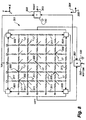
- FIG. 8 is a top view that is taken in the X-Y plane showing an embodiment of this invention having four corner-located current mirrors and adders, or current-buffers 601-604, wherein the amplifier output 17 of each of 25 node-cells 2 is connected to a different one of the 25 nodes 300 of a resistive network 301, each node 300 being established by the intersection of a cell-column C1-C5 with a cell-row R1-R5.
- Resistive network 301 comprises a pseudo-resistive network having four corner-located current mirrors and adders, or current buffers 601-604, that operates to detect the mass or area and the centroid 470 of the blob signals 170 that are shown in the various ones of figures 5.
- FIG. 9 shows one individual resistor-network node 300 connected to the output 17 of its corresponding individual FIG. 2 node-amplifier.
- FIG. 9 also shows four resistors 311 that connect this node 300 to its four adjacent nodes 300.
- node 300 of FIG. 9 is the node that is formed by the intersection of node-column C2 and node-row R2
- its amplifier output 17 is the output of the FIG. 2 amplifier that is associated with the FIG. 1 cell that is located at the intersection of cell-column 2 and cell-row 2.
- array 3 of FIGS. 1-3 is first used to acquire user-fingerprint-ID during log-on, as was described relative to FIG.4. Thereafter, output 17 of each of the 25 cell-amplifiers of FIG. 2 is connected to a corresponding one of the 25 resistor-nodes 300 shown in FIG. 8.
- electrical outputs 302 and 303 respectively, provide the X-direction component and the Y-direction component of an output signal that defines the user's desired cursor/pointer screen movement direction.
- signals 302,303 are used to control movement of a cursor/pointer across a TV or monitor screen, with this movement being continuous by virtue of a static/non-moving position of a fingertip 18 on the surface of the FIG. 8 touchpad.
- outputs 302,303 provide an analog value which is proportional to the zero and first moment of the 2D-pattern.
- output 302 is essentially of zero magnitude, whereas output 303 is of a given magnitude and a given polarity or signal sense. As a result, upward cursor movement 171 is produced. If it is now assumed that the fingertip position produces bright blob 170 of FIG. 5C, then output 302 remains essentially zero, whereas output 303 is now of a given magnitude, but of an opposite polarity or signal sense, and downward cursor movement 172 results. In a like manner, outputs 302,303 can be related to the cursor movements as explained relative to the remaining ones of figures 5.
- the user achieves a desired cursor/pointer movement by sidewise rolling movement of fingertip 18, represented by arrow 304, and/or by lengthwise end to end pitching of fingertip 18, represented by arrow 305.
- each individual cell output 17 of the array is serially scanned.
- the touchpad's individual cell outputs 17 are not scanned. Rather, each individual cell output 17 is connected to an individual node 300 of row/column resistive network 301.
- Array 301 generates a X-direction cursor/pointer movement command 302, that is a horizontal left/right screen movement command, as fingertip 18 is moved, or rolled, sideways on the upper horizontal surface of array 301, this movement being indicated by arrow 305.
- Array 301 generates a Y-direction cursor/pointer movement command 303 that is a vertical up/down screen movement command, as fingertip 18 is moved, or pitched, end to end on the horizontal upper surface of array 301, this movement being indicated by arrow 304.
- Array 301 also generates a switch output or Z-command output as long as fingertip 18 is pressed vertically down onto the general geometric center of the current position of fingertip 18 on the horizontal upper surface of array 301.
- one step in enabling touchpad operation may be to switch each FIG. 2 node-amplifier 13 from low gain to high gain by operation of a change in the magnitude of the voltage Vr of FIG. 1.
- the composite electrical outputs 17 of all node-amplifiers 13 can be described as an electronic array picture having a blob 170 that is located on a dark background wherein the central position 470 of this blob on the dark background corresponds to the area of contact of fingertip 18 with the top horizontal surface of array 301.
- the first-moment coordinates of the position of this blob 170, or brightness function within this electronic picture encodes the X and Y displacement or finger position on the array's top surface, while the zero-moment value of bright blob 170 encodes the finger's downward, or Z-direction pressure function.
- Networks 307 and 308 of FIG. 8 operate to determine the first-moment-coordinates and the zero-moment-value that are encoded within this electronic picture.
- the entire electronic image of the array that is all cell-amplifier output signals 17, is transferred into a computation system where the first-moment-coordinates and the zero-moment-value (also called “mass” and “centroid") are calculated using hardware or software.
- analog computation may be performed on the FIG. 8 analog values that are proportional to the zero and first moment of the 2-D pattern.
- the resistor-network embodiment of the invention utilizes the first above-mentioned technique by way of the following hardware.
- the two-dimensional (2D) electronic signal-picture, output, or pattern of array 3 which encodes the touching function of fingertip 18 on the array's upper surface, is injected into nodes 300 of the 2D resistive network 301 of FIG. 8.
- Networks 307,308,309 then function to detect the centroid and the mass of this array output signal.
- the functions centroid and mass are calculated simultaneously by the FIG. 8 arrangement.
- each node 300 is connected to its adjacent nodes 300 by way of a resistor 311. While the resistance values, or magnitudes of resistors 3 11 are not critical, all resistors 311 should be of generally the same resistance value or magnitude. In addition, and as stated above, as a feature of the invention, resistors 311 1 are implemented by way of MOS transistors.
Description
- US. Patent Application Serial No. 08/799,548 (cited within US Patent No. 6114862 issued on 5 September 2000 as a continuation in-part from US Patent Application Serial No. 08/799,548) by Marco Tartagni, filed February 13, 1997, and entitled CAPACITIVE DISTANCE SENSOR is hereby referenced. This application described an Integrated Circuit (IC) capacitive distance sensor having a number of uses, including fingerprint acquisition. In this solid-state IC device, a portion of which is shown in FIGS. 1-3 of the present application, each
individual cell 2 of amulti-cell array 3 includes a pair offlat metal armatures cell 2 also includes the amplifier means shown in FIG. 2 whereinamplifier input 16 is connected to onearmature 24, and whereinamplifier output 17 is connected to theother armature 23, to thereby provide anegative feedback circuit - This invention relates to the field of the manual control of a cursor, or pointer on a display screen, such as a computer display monitor or a television (TV) set.
- The prior art provides two general types of devices that achieve screen cursor/pointer movement control.
- In a first type of device, of which a mouse is an example, continuous manual movement of the mouse across a generally horizontal surface is required in order to produce a continuous and corresponding direction of movement of the cursor/pointer across the display screen. This cursor/pointer movement stops when movement of the mouse stops. When the cursor/pointer must be moved a large screen distance, it is usually necessary to lift the mouse off of the surface, and then retrace the mouse over the horizontal surface one or more times.
- In a second type of device, of which a joystick is an example, as long as the joystick is manually held in an off-center position, the cursor/pointer continuously moves in a corresponding direction across the screen. In order to stop this cursor/pointer movement, the joystick is returned to its center or neutral position.
- The present invention will be described relative to embodiments of a fingertip operated capacitance touchpad whose end-result operation is generally the same as a joystick; however, the scope of the invention is not to be limited in this manner. That is, a fingertip position on the capacitance touchpad of the present invention produces cursor/pointer screen movement in accordance with the fingertip's position. The present invention finds particular utility in replacing glidepoint and trackpoint devices often found in portable computers, such as laptop computers and palmtop computers.
- Embodiments of the present invention relate to a use of, and modifications to, a capacitance distance/fingerprint sensor, such as is described in the above-mentioned related patent application. The general use of capacitance-type sensors is known.
- For example, the publication SENSORS AND ACTUATORS, Jan/Feb 1989, no. 1/2, at pages 141-153, contains an article entitled INTEGRATED TACTILE IMAGER WITH AN INTRINSIC CONTOUR DETECTION OPTION that was presented at the Fourth International Conference on Solid-State Sensors and Actuators (Transducers '87), Tokyo, Japan, June 2-5, 1987.
- This article describes an integrated capacitive tactile imaging sensor that comprises a multi-layer construction having a bottom ceramic support, a 9-row/9-column array of square aluminum electrodes that are contained on a silicon wafer integrated circuit, a flexible and isolating intermediate layer that is made up of natural rubber, a thin conductive rubber layer, and a top protective layer. In this device, capacitance depends upon local deformation of the natural rubber layer. The 81 individual aluminum electrodes of this device provide capacitive measurement of an indentation pattern within the natural rubber layer, this indentation being caused by a pressure distribution that acts on the top protective layer.
- The use of a capacitance-type sensor to sense the minutiae of a fingerprint is also known.
- For example, the publication IEEE ELECTRON DEVICE LETTERS, VOL. 18,
NO 1, January 1997, pages 19-20, contains an article entitled NOVEL FINGERPRINT SCANNING ARRAYS USING POLYSILICON TFT'S OF GLASS AND POLYMER SUBSTRATES. This article describes a two-dimensional (2-D), 200x200, capacitance sensing array that is made up of 40,000 individual pixels. Each pixel of the array includes two Thin Film Transistors (TFTs) and a capacitor plate. Each array pixel resides at the intersection of an array-row and an array-column, and each array pixel is individually addressable by way of row-driver circuits and column-driver circuits. - Considering the two TFTs, hereinafter called TFT-A and TFT-B that are associated with a given pixel, the drain electrodes of TFT-A and TFT-B are connected to the pixel's capacitor plate, the gate electrode and the source electrode of TFT-A are connected to a row-conductor that is associated with the pixel, the gate of TFT-B is connected to the following row-conductor, and the source of TFT-B is connected to a column-conductor that is associated with the pixel.
- A thin (0.1 micrometer) silicon nitride insulator overlies the capacitor plate of each array pixel. When the ridge of a fingerprint lies directly over the capacitor plate, a capacitor is formed between the capacitor plate and the finger. This capacitor is charged when a row-pulse (8 to 10 VDC, and of 10 to 100 microsecond duration) is applied to the pixel by way of the row conductor that is associated with this pixel and TFT-A. This stored charge is thereafter transferred onto the pixel's column-conductor through TFT-B when a row-pulse is applied to the following row-electrode.
- Also of interest is the publication 1997 IEEE INTERNATIONAL SOLID-STATE CIRCUITS CONFERENCE that contains an article beginning at page 200 entitled A 390DPI LIVE FINGERPRINT IMAGER BASED ON FEEDBACK CAPACITIVE SENSING SCHEME. This article describes a single-chip, 200x200 element array, 2-metal digital CMOS technology sensor that is based upon feedback capacitance sensing, and that operates to detect the electrical field variation that is induced by the finger's skin surface. In each element of the array, two horizontally spaced metal plates are separated from the overlying and adjacent portion of the finger's skin surface by passivation oxide. Since the distance between the skin and the sensor's surface identifies the presence of the fingerprint's ridges and valleys, an array of elements provides a complete fingerprint pattern.
- In each element of the array, the two metal plates are respectively connected to the input and the output of a high-gain inverter, to thereby form a charge integrator. In operation, the charge integrator is first reset by shorting the input and output of the inverter. A fixed amount of charge is then sinked from the input, causing the output voltage to swing inversely proportional to a feedback capacitance value that is inversely proportional to the distance to the fingerprint's ridges and valleys. The array of cells, or sensors, thus provides the complete fingerprint pattern. The fingerprint image disappears when the finger is removed from the array.
- U.S. Patent 4,353,056, hereby referenced, is of interest in that it relates to a capacitance-type fingerprint sensor wherein a finger is pressed onto the surface of the sensor in order to read the ridges and valleys of the fingerprint. The sensor surface has a large number of capacitors of a small physical size associated therewith. Two sensors are described. In a first type of sensor, an electrical insulator carries a number of flexible and horizontally spaced curved metal electrodes, and two adjacent metal electrodes which comprise one capacitor. A protective insulating film overlies the electrical insulator, and when a finger is brought into physical contact with this protective insulating film, the metal electrodes are physically deformed, thereby selectively changing the capacitance of the large number of capacitors in accordance with the fingerprint's ridge/valley pattern. In a second type of sensor, the top surface of a rigid support carries a number of horizontally spaced and flat metal electrodes in a fixed position. Placed above the plane of the metal electrodes is the sequential arrangement of a flexible insulator, a flexible electrode, and a flexible protective membrane. A capacitor is formed between the top flexible electrode and each of the lower and fixed position flat metal electrodes. When the end of a finger is brought into contact with the flexible membrane, the flexible electrode becomes wavy in accordance with the fingerprints' ridges/valleys pattern.
- In addition, U.S. Patent 5,325,442, hereby referenced, relates to a capacitance-type fingerprint sensor having a sensing pad that comprises a planar array of row/column sensing elements having a pitch of about 100-micrometers. Each sensing element is located at the intersection of a row conductor and a column conductor, and in each sensing element, a sensing capacitor comprises a planar sensing electrode that is spaced from a finger surface by way of an insulating film that overlies the sensing electrode. The plurality of sensing electrodes that make up the array are regularly spaced and equal size rectangles.
- The sensing elements are fabricated using photolithographic processes, and each individual sensing element includes a Thin-Film-Transistor (TFT) in the form of a Field-Effect-Transistor (FET). Each FET gate is connected to a row conductor, each FET source is connected to a column conductor, and each FET drain is connected to a sensing electrode.
- In one embodiment, each sensing element comprises a sensing capacitor that is formed between a sensing electrode and the finger. In another embodiment, each sensing element includes an electrically isolated and conducting pad that is physically engaged by the finger.
- European patent application EU 96830068.1 (EP790479) is also of interest. This application discloses an array of capacitance sensors that are operable to detect the fingerprint pattern of a finger that is touching the top or upper surface of the array.
- U.S. Patent Nos. 5,374,787, 5,495,077, and 5,648,642 are of interest in that they provide object/proximity detectors having a plurality of sensor pads/lines that are disposed in a row/column matrix.
- U.S. Patent 5,543, 588 is of interest in that it discloses a hand-held device having a disposed screen on one side thereof and a touch sensitive transducer disposed on the opposite side.
- U.S. Patent Nos. 5,543,590 and 5,543,591 are of interest in that they disclose a device for moving a cursor on a display screen wherein a sensing plane includes a matrix of row/column oriented conductor lines.
- While prior devices as above described are generally useful for their limited intended purposes, a need remains in the art for a capacitance-type touchpad that operates to simulate a joystick or a mouse wherein the position of a fingertip on the upper surface of the capacitance touchpad produces cursor/pointer screen movement.
- This invention may be based upon the use of a matrix array of capacitance sensors; for example, a matrix array as is shown in above-mentioned European patent application BU96830068.1 (EP790479).
- The array of this invention can be initially used to acquire a user fingerprint; for example, as a user-identification (ID) procedure that occurs during log-on to a device, such as a laptop or a palmtop computer. Subsequent operation of the computer often requires control of the movement of a cursor across a display screen. The array of this invention also provides this cursor movement.
- That is, when a user first logs onto the computer, the array of this invention captures a fingerprint pattern that is used to determine user authorization. Thereafter, the array is used to provide screen cursor/pointer control, with the cursor/pointer moving across the screen by virtue of the position of a fingertip on the upper surface of the array. This fingertip position is achieved, after fingerprint acquisition, only by rolling and/or pitching the fingertip on the top surface of the array. In an embodiment of the invention, cursor/pointer movement stops when the fingertip is removed from the array, or when the fingertip is moved to a mid-position on the top surface of the array.
- During log-on, when the user is being identified/verified by comparing a sensor-acquired fingerprint pattern to memory-stored fingerprint patterns, the individual cell output of the array is serially scanned. Thereafter, and as the array is used in accordance with this invention, in order to achieve screen cursor/pointer control, the individual cell output of the array need not be scanned. Rather, each individual cell output of the array is connected to a corresponding individual node of a row/column resistive network.
- While embodiments of the invention will be described relative to features, such as cursor control, utility is also found in aplications such as ATM machines, wherein user fingerprint authorization is first obtained, followed by using the array as an input device for choice selection and Yes/No responses to the ATM machine.
- The sensing array of this invention can also be used as a pointing device in a 3D virtual reality application, in which case, the array is mounted over a structure that follows the movement of the fingers of a user's hand. In this way, a user is enabled to make selections using a finger and a 3D virtual menu, and in 3D virtual games, the array can be used to sense planar X,Y direction as well as Z direction commands.
- The array of this invention provides X-direction cursor/pointer movement commands (i.e., left/right screen movement commands) as the fingertip is moved, or rolled sideways, on the array's upper surface. The array of this invention provides Y-direction cursor/pointer movement commands (i.e., up/down screen movement commands) as the fingertip is moved or pitched end to end on the upper surface of the array. The array of this invention provides Z-information, or switch-closed information, as the fingertip is pressed vertically down into the upper surface of the array. The upper surface of the array of this invention is about 1 cm square, and usually cooperates with the tip of a user's index finger.
- When the gain of such a capacitance fingerprint sensing cell (for example, as is shown in the above-mentioned EU patent application) is adjusted to be high, or when the resolution of the array is low, the electrical output of the array is a two-dimensional "electronic picture" having a bright blob on a dark background. The position of the blob within this electronic picture corresponds to the contact area of the fingertip with the upper surface of the sensor.
- The first moment coordinates of the position of this blob, or brightness function, encodes the X displacement and the Y displacement, or the fingertip position on the upper surface of the array, while the zero-moment value of this brightness function encodes the fingertip's downward pressure function.
- In order to calculate the X output and Y output of the array, two options are available. First, the entire electronic image of the array, or picture, is transferred into a computation system where these two outputs (also called "mass" and "centroid") are calculated using hardware or software techniques. Second, analog computation is performed directly on the picture output of the sensor.
- Relative to FIG. 8, the two-dimension (2D) electronic signal output, or pattern of the array which encodes the touching function of a fingertip on the upper surface of the array, is injected into a 2D pseudo-resistive network, as shown in FIG. 8. This network now detects the centroid, or first-moment and mass, or second moment of the incoming array output signal. The functions centroid and mass are calculated simultaneously by the FIG. 8 arrangement.
- In accordance with a feature of this invention, the pseudo-resistive network of FIG. 8 can be embedded within the sensor array of FIG. 1 using integrated circuit techniques, to thereby provide an integrated device. For example, each resistor of FIG. 8 can be implemented with a MOS transistor, as taught and illustrated in an article by M. Tartagni and P. Persona entitled "COMPUTING CENTROIDS IN CURRENT-MODE TECHNIQUE" in the publication ELECTRIC LETTERS (29 (21), 1811-1813, October 1993.
- There is provided according to the present invention a capacitance touchpad according to
claim 1. - While the invention will be described while making comparisons to the well-known joy-stick type of device, those skilled in the art will recognize that the invention also finds utility in replacing mouse-like devices.
- These and other object, features and advantages of this invention will be apparent to those of skill in the art upon reference to the following detailed description of preferred embodiments of the invention, which description makes reference to the drawing.
- FIGS. 1, 2 and 3 relate to the above-mentioned related U.S. patent application, and are used in embodiments of this invention.
- FIG. 4 is a flowchart that shows a fingerprint pattern acquisition process whereby a FIG. 1-3 arrangement is initially used during an initial user authorization log-on procedure, which user thereafter uses a version of the FIG. 1-3 arrangement in capacitive touchpad arrangements of the present invention in order to generate a cursor/pointer screen directional movement control signal.
- FIGS. 5A through 51 show a two-dimensional (2D) electrical picture signal that is generated by the capacitance touchpad of this invention for various positions of a fingertip on the touchpad upper surface, each of these figures having a mass outline and a centroid-dot that is located within the mass outline.
- FIG. 6 shows the Y-direction pitching of a fingertip end to end on the touchpad upper surface.
- FIG. 7 shows the X-direction rolling of a fingertip side to side on the touchpad upper surface.
- FIG. 8 is a circuit embodiment of this invention wherein the amplifier output signal from each of 25 sensor cells of a modified FIG. 1 are connected to a corresponding one of 25 resistor nodes within a row/column resistor network or array.
- FIG. 9 shows one individual resistor node of FIG. 8 connected to receive the output of a corresponding individual amplifier of the type shown in FIGS. 2-3, FIG. 9 also showing four resistors that interconnect this resistor-node to adjacent resistor nodes.
- The various figures are provided with a X-Y-Z three-dimensional coordinate system, and with legends reading top, bottom, left and right, in order to relate the various figures one to the other, and in order to relate the direction of screen cursor/pointer movement to certain of the figures.
- FIGS. 1, 2 and 3 correspond to the above-mentioned related U.S. patent application, and versions thereof are usable in embodiments of the present invention.
- FIG. 1 is a top view of an
IC device 1 that includes a generally planar, multiple pixel, multiple row/column,array 3 having a relatively large number of solid state capacitive sensor cells, ornodes 2, that operate to provide a serial signalelectrical output 10 that comprises a multiple pixel fingerprint pattern, or electrical signal picture of a fingerprint. As shown, FIG. 1 is taken in the X-Y plane. -
Array 3 contains the number N of horizontal or X-direction extending rows ofindividual nodes 2. Each row has the number M ofindividual nodes 2 therein.Array 3 thus contains the number M of vertically or Y-direction extending columns ofindividual nodes 2, and each column has the number N ofindividual nodes 2 therein. The numbers N and M are integers that may or may not be equal to each other. The number of individual picture elements, pixels, nodes, orcells 2 withinarray 3 is quite large for fingerprint pattern acquisition, and equals the product of MxN. An example is 512x512 pixels, nodes, orcells 2 withinarray 3,array 3 being of a physical size of about 20 mm to about 25 mm. - FIG. 2 shows a
fingertip 18 in physical contact with the upper andactive surface 125 ofarray 3. - During fingerprint pattern acquisition, each
individual cell 2 that is withinarray 3 is addressable by virtue of each cell being physically located at a unique intersection of a row/column ofarray 3. The manner in which theindividual cells 2 ofarray 3 are addressed and read out in order to digitize a fingerprint pattern are well known to those of skill in the art, and do not form a limitation on this invention. -
IC device 1 includes a horizontal scanning stage, ornetwork 6, and a vertical scanning stage ornetwork 5 for sequentially interrogating, or reading, onecell 2 at a time during fingerprint pattern acquisition according to a predetermined scanning pattern. Preferably, stages 5 and 6 comprise shift registers, or decoders, that operate to interrogate the FIG. 2outputs 17 ofcells 2 in a time sequence. -
IC device 1 also includes a supply/logic stage ornetwork 7 that operates to supply the IC device components, including allcells 2, with necessary operating voltages, and to control the sequence of steps that are necessary for operation ofIC device 1. In particular, aDC voltage source 12 provides a DC reference voltage Vr that is referenced to ground potential at 100. A buffer 8 is connected to theoutputs 17 of allcells 2.Output 10 of buffer 8 comprises the sequentially arranged output signal ofIC device 1, the signal atoutput 10 being controlled by operation ofscanning stages - FIG. 2 schematically shows the circuit of a
single cell 2 of thearray 3 of FIG. 1. Allcells 2 are generally identical in construction and arrangement. Eachcell 2 includes a low-power, signal inverting, node-amplifier 13 having an exemplary gain from about 3000 to about 4000. -
Terminal 21 comprises the input to the circuit of acell 2, and terminal 21 andinput capacitor 20 connect to input 16 ofamplifier 13.Terminal 17 comprises the output ofcell 2 and itsamplifier 13. Eachcell 2 also includes two X-Y planar armatures, ormetal capacitor plates - A
thin dielectric layer 25 coverscapacitor plates horizontal surface 125 oflayer 25 provides an active array surface for physical contact by theskin surface 18 of a finger whose fingerprint is to be sensed, determined or acquired.Dielectric layer 25 may cover the entire face of the upper portion of IC device I that includesarray 3 and itsindividual cells 2. - In use for fingerprint pattern acquisition, a
fingertip 18 is placed on theupper surface 125 of thedielectric layer 25 ofarray 3.Skin surface 18 thereby forms an armature, or electrode, that vertically overlies and faces the top, X-Y planar, surfaces ofcapacitor plates Skin surface 18 operates to define withplates 23,24 a first capacitor 34, as shown in FIG. 3, and asecond capacitor 33 as shown in FIG. 3. Series connectedcompound capacitors 33,34 are connected in negative feedback fashion fromamplifier output 17 toamplifier input 16. - Each FIG. 2 node-
amplifier 13 also includes a normally-open start, reset, or controlswitch 19, preferably in the form of a MOS switch.Switch 19 selectively and momentarily operates toshort amplifier input 16 toamplifier output 17.Switch 19 is controlled by a control signal "R" that is provided by the supply andlogic unit 7 of FIG. 1. At the start of a fingerprint acquisition operation, switches 19 of allarray cells 2 are momentarily closed, and the voltage level at allcell inputs 21 is thus maintained at a constant magnitude. In this way, the input voltage of allcells 2 is brought to the same potential as the cell's output voltage. - Shortly thereafter, supply and
logic unit 7 operates to open all reset switches 19, and to supply allcell inputs 21 with a step voltage that is equal in magnitude to reference voltage Vr. An electrical charge is now induced at each of thecell input capacitors 20, thus permitting the reading of the local and individual Z-direction cell distances "d" that exist between a cell'scapacitor plates skin surface 18 of the cell. - Scanning stages 5,6 of FIG. 1 now operate to sequentially enable the reading or interrogation of the
many cells 2 withinarray 3. In this way, buffer 8 operates to sequentially provide anoutput 10 in the form of a sequence of gray levels of voltage that provide a three-dimensional readout, and display of theskin surface 18 of the finger that is currently resident on thetop surface 125 ofarray 3. - FIG. 3 is an equivalent circuit of the single cell circuit shown in FIG. 2. The input capacitance of
amplifier 13 is shown at 30, the output capacitance ofamplifier 13 is shown at 31, and the two above-mentioned series connected and skin-sensitive capacitors are shown at 33,34. - In accordance with a feature of this invention, the gain of each
amplifier 16 can be increased in order to provide an output signal from the FIG. 1 array that comprises the correctedshape 170 shown in the various areas of FIGS. 5A-51. However, this increased gain feature is not required, since this corrected shape can also be calculated over the fingertip's complicated fingerprint pattern because the center of mass of the group of objects comprising the fingerprint is positioned in the center of the group of objects. When the increased gain feature is desired it is implemented by a step change in the magnitude of the voltage Vr of FIG. 1. - In use as a capacitance touchpad in accordance with the scope of this invention, the
output 17 of allcells 2, or node-amplifiers 13, is a picture-signal that appears as abright blob 170 that is positioned on a dark background, as is shown in FIGS. 5A-51. The position of thisblob 170 within the picture encodes the contact area/position offinger 18 with thetop surface 125 of the capacitance touchpad. This bloboutput signal function 170 can also be achieved by a construction and arrangement that ensures that the resolution of the cell-array matrix is low. - FIG. 4 is a flowchart that shows a fingerprint pattern acquisition process, whereby the arrangement of FIGS. 1-3 is used in a low-gain mode during an initial log-on by a computer user, which user thereafter uses the capacitance touchpad construction and arrangement of the present invention to generate a cursor/pointer screen direction/movement control signal, and/or a switch on/off the touchpad signal.
- During this fingerprint pattern acquisition process, the
buffer output 10 fromarray 3 of FIG. 1 is connected to aprocessing unit 160. In the sequence of operation, start switches 19 of allcells 2 are momentarily closed, thereafter reference step pulse voltage Vr is applied to allamplifier inputs 21, and thereafter allcell outputs 17 are presented to bufferoutput 10 in accordance with a sequence that is established by vertical andhorizontal scan networks fingertip 18 is presented as aninput 10 toprocessing unit 160.Connection 10 betweenarray 3 andprocessing unit 160 is shown to be bi-directional in order to signify the changing of array sensitivity when changing from fingerprint acquisition to touchpad operation. - Reference memory 161 contains a number of previously-stored fingerprint patterns; for example, one fingerprint pattern for each authorized user. At
step 163, a similar computing unit comparesinput 10 to the patterns that are contained inmemory 162, and when a pattern match is detected, the identity of the current touchpad/computer user is recorded in workingmemory 164. - As will be apparent, after the identity of the current touchpad/computer user has been established,
step 165 enables use of the touchpad of this invention as a joystick-type touchpad. As mentioned previously, this joystick-type use of the touchpad takes place in a high-gain mode of FIGS. 1 -3. - When the capacitance touchpad of this invention is used in its high-gain mode to achieve cursor/pointer control on a display screen, the
composite outputs 17 of allarray cells 2 comprises an electronic picture-signal that appears as a bright blob that is positioned on a dark background. - FIGS. 5A through 51 show such a picture-signal for various positions of a
fingertip 18 onarray surface 125. The position ofbright blob 170 in each of these figures corresponds to the contact area, or position offingertip 18 with thetop surface 125 of the capacitance touchpad. The center of eachblob 170 is shown at 470. As stated previously, a Z-direction depression offingertip 18 when it is in any of the FIG. 5A-5I positions, modifies or enlarges the mass ofbright blob signal 170, so as to provide a switch-closed signal. - In FIG. 5A, the
fingertip center 470 is located in a mid-position onarray surface 125, and in this position, no cursor movement is produced. However, the relatively large mass, or size ofblob 170 that is shown in FIG. 5A, is indicative of a switch-closed condition that is produced by pressingfingertip 18 vertically down ontoarray surface 125. - FIG. 6 represents the Y-direction pitching of
fingertip 18 end to end onsurface 125. In accordance with the direction of this pitching movement, abright blob 170 is produced, as is shown in FIGS. 5B and 5C. That is, the pitching offingertip 18 downward in FIG. 6 produces the condition shown in FIG. 58, and upward cursor movement occurs, as is represented byarrow 171. However, when the FIG. 6 pitching offingertip 18 upward produces the condition of FIG. 5C, downward cursor movement as represented byarrow 172 occurs. - FIG. 7 represents the X-direction rolling of
fingertip 18 side to side onsurface 125. In accordance with the direction of this rolling movement, ablob 170 is produced, as is shown in FIGS. 5E and 5D. That is, the rolling offingertip 18 to the left in FIG. 7 produces the condition shown in FIG. 5E, and leftward cursor movement occurs, as is represented byarrow 173. However, when the rolling offingertip 18 to the right produces the condition of FIG. 5D, rightward cursor movement as represented byarrow 174 occurs. - In a like manner, FIGS. 5F and 5G show how
diagonal cursor movements fingertip 18 in one diagonal direction onsurface 125, whereas FIGS. 5H and 5I s show howdiagonal cursor movements fingertip 18 in an orthogonal diagonal direction onsurface 125. - FIG. 8 is a top view that is taken in the X-Y plane showing an embodiment of this invention having four corner-located current mirrors and adders, or current-buffers 601-604, wherein the
amplifier output 17 of each of 25 node-cells 2 is connected to a different one of the 25nodes 300 of aresistive network 301, eachnode 300 being established by the intersection of a cell-column C1-C5 with a cell-row R1-R5.Resistive network 301 comprises a pseudo-resistive network having four corner-located current mirrors and adders, or current buffers 601-604, that operates to detect the mass or area and thecentroid 470 of the blob signals 170 that are shown in the various ones of figures 5. - FIG. 9 shows one individual resistor-
network node 300 connected to theoutput 17 of its corresponding individual FIG. 2 node-amplifier. FIG. 9 also shows fourresistors 311 that connect thisnode 300 to its fouradjacent nodes 300. For example, ifnode 300 of FIG. 9 is the node that is formed by the intersection of node-column C2 and node-row R2, then itsamplifier output 17 is the output of the FIG. 2 amplifier that is associated with the FIG. 1 cell that is located at the intersection of cell-column 2 and cell-row 2. - In this embodiment of the invention,
array 3 of FIGS. 1-3 is first used to acquire user-fingerprint-ID during log-on, as was described relative to FIG.4. Thereafter,output 17 of each of the 25 cell-amplifiers of FIG. 2 is connected to a corresponding one of the 25 resistor-nodes 300 shown in FIG. 8. - In the FIG. 8 mode of operation,
electrical outputs fingertip 18 on the surface of the FIG. 8 touchpad. - As taught by D. L. Standley in an article entitled "An Object Position and Orientation IC with Embedded Imager" in the IEEE Journal of Solid State Circuits (26, 1853-1858, December 1991), outputs 302,303 provide an analog value which is proportional to the zero and first moment of the 2D-pattern.
- With reference to FIGS. 5B and 5C, if it is assumed that a fingertip position produces
blob 170 of FIG. 5B, thenoutput 302 is essentially of zero magnitude, whereasoutput 303 is of a given magnitude and a given polarity or signal sense. As a result,upward cursor movement 171 is produced. If it is now assumed that the fingertip position producesbright blob 170 of FIG. 5C, thenoutput 302 remains essentially zero, whereasoutput 303 is now of a given magnitude, but of an opposite polarity or signal sense, anddownward cursor movement 172 results. In a like manner, outputs 302,303 can be related to the cursor movements as explained relative to the remaining ones of figures 5. - As stated previously, the user achieves a desired cursor/pointer movement by sidewise rolling movement of
fingertip 18, represented byarrow 304, and/or by lengthwise end to end pitching offingertip 18, represented byarrow 305. - During log-on, when the user is being identified/verified by comparing an acquired fingerprint pattern to the memory-stored
fingerprint patterns 162 of FIG. 4, the individual cell outputs 17 of the array are serially scanned. However, thereafter, and as the array is used in accordance with this invention to achieve screen cursor/pointer control, the touchpad's individual cell outputs 17 are not scanned. Rather, eachindividual cell output 17 is connected to anindividual node 300 of row/columnresistive network 301. -
Array 301 generates a X-direction cursor/pointer movement command 302, that is a horizontal left/right screen movement command, asfingertip 18 is moved, or rolled, sideways on the upper horizontal surface ofarray 301, this movement being indicated byarrow 305.Array 301 generates a Y-direction cursor/pointer movement command 303 that is a vertical up/down screen movement command, asfingertip 18 is moved, or pitched, end to end on the horizontal upper surface ofarray 301, this movement being indicated byarrow 304.Array 301 also generates a switch output or Z-command output as long asfingertip 18 is pressed vertically down onto the general geometric center of the current position offingertip 18 on the horizontal upper surface ofarray 301. - As previously stated, one step in enabling touchpad operation, as shown at
step 165 of FIG. 4, may be to switch each FIG. 2 node-amplifier 13 from low gain to high gain by operation of a change in the magnitude of the voltage Vr of FIG. 1. When each node-amplifier 13 operates at this high gain, or in the alternative, when the resolution ofarray 301 is low, the compositeelectrical outputs 17 of all node-amplifiers 13 can be described as an electronic array picture having ablob 170 that is located on a dark background wherein thecentral position 470 of this blob on the dark background corresponds to the area of contact offingertip 18 with the top horizontal surface ofarray 301. - The first-moment coordinates of the position of this
blob 170, or brightness function within this electronic picture, encodes the X and Y displacement or finger position on the array's top surface, while the zero-moment value ofbright blob 170 encodes the finger's downward, or Z-direction pressure function.Networks - In order to calculate the two X and Y array outputs 302,303, two options are available. First, the entire electronic image of the array, that is all cell-amplifier output signals 17, is transferred into a computation system where the first-moment-coordinates and the zero-moment-value (also called "mass" and "centroid") are calculated using hardware or software. Second, analog computation may be performed on the FIG. 8 analog values that are proportional to the zero and first moment of the 2-D pattern.
- The resistor-network embodiment of the invention utilizes the first above-mentioned technique by way of the following hardware. Relative to FIG. 1, the two-dimensional (2D) electronic signal-picture, output, or pattern of
array 3, which encodes the touching function offingertip 18 on the array's upper surface, is injected intonodes 300 of the 2Dresistive network 301 of FIG. 8. Networks 307,308,309 then function to detect the centroid and the mass of this array output signal. The functions centroid and mass are calculated simultaneously by the FIG. 8 arrangement. - As shown in FIG. 8, each
node 300 is connected to itsadjacent nodes 300 by way of aresistor 311. While the resistance values, or magnitudes ofresistors 3 11 are not critical, allresistors 311 should be of generally the same resistance value or magnitude. In addition, and as stated above, as a feature of the invention,resistors 311 1 are implemented by way of MOS transistors. - While the above description assumes that a fingerprint pattern is first acquired, and touchpad use is thereafter enabled, it is also possible in accordance with the scope of this invention, that cursor/pointer control by virtue of finger rotation/position can be detected concurrently as the fingerprint pattern itself is detected.
- The above detailed description of embodiments of this invention is not to be taken as a limitation on the scope of this invention, since it is apparent that those skilled in the related art will, upon reading this detailed description, readily visualize yet other embodiments that are clearly within the scope of this invention.
Claims (11)
- A capacitance touchpad for providing an electrical output signal for selectively controlling the movement of visual pointer indicia across a two dimensional display screen, comprising:a plurality N of individual capacitance sensing cells (2) arranged in a first two dimensional row/column array (3), said first array (3) having N row/colomn intersections, and said first array (3) occupying a generally planar that area is adapted to cooperate with a human fingertip to produce an output signal for controlling said indicia movement, each individual sensing cell (2) having a unique output signal that varies in accordance with a positional relationship with a human fingertip;a plurality N of individual resistance nodes (300) arranged in a second two dimensional row/column array (301), said second array having N row/column intersections in a configuration that corresponds to said N row/column intersections of said first array;circuit means connecting each unique output signal of said sensing cells (2) to a corresponding one of said resistance nodes (300) of said second array;first computation means connected to said second array (301) for computing a centroid output signal as a function of the position of a human fingertip on said planar area of said first array (3); andfirst output means connected to said first computation means and providing an indicia movement control signal as a function of said centroid output signal.
- The capacitance touchpad of claim 1, including:second computation means connected to said second array for computing a mass output signal as a function of an area occupied by a human fingertip on said planar area; andsecond outut means connected to said second computation means providing a switch on/off signal as a function of said mass output signal.
- The capacitance touchpad of claim 1, wherein:the first array (3) has a sensing surface (125);adapted to receive the human fingertip and to control movement of the indicator indicia as a function of a position of the human fingertip on said sensing surface.
- The capacitance touchpad of claim 3, wherein each of said N sensing cells having an amplifier with an amplifier (13) input (16) and an amplifier output (17), a first and a second physically spaced capacitor plate (23, 24) associated with said sensing surface (125).
- The capacitance touchpad of claim 3, including:second computation means connected to said second array (301) for computing a mass output signal as a function of an area occupied by the human fingertip on said sensing surface (125); andsecond output means connected to said second computation means and providing a switch on/off signal as a function of said mass output signal.
- The capacitance touchpad of claim 3, further comprising:user-authorization means connected to said first array and operable to generate a user fingerprint pattern for comparison to authorized user fingerprint patterns, and to thereby enable operation of said touchpad to control movement of the cursor as a function of a position of the human fingertip on said sensing surface (125).
- The capacitance touchpad of claim 1, wherein the first array (3) comprises;
a generally flat dielectric sensing surface (125) having a plurality of surface-portions;
said sensing surface (125) being adapted to be physically touched by the human fingertip; said plurality N of sensing cells being associated with said surface-portions,
said sensing cells (2) being arranged in a cell array having R rows and C columns, said rows and columns forming RxC intersections with one of said sensing cells being located at each of said intersections and at a corresponding surface portion;
each of said sensing cells (2) having an amplifier (13) with an amplifier input (16) and an amplifier output (17);
each of said sensing cells (2) having a first (24) and a second (23) physically spaced capacitor plate associated with, but isolated from said corresponding surface portion;
each of said sensing cells (2) having said first capacitor plate (24) connected to said amplifier input (16) and said second capacitor plate (23) connected to said amplifier output (17), to thereby provide a negative input to output amplifier feedback signal as a function of said human fingertip touching said corresponding surface-portion; - The capacitance touchpad of claim 7, wherein the plurality N of resistance nodes arranged in a two dimensional array (301) having R rows and C columns, said rows and columns forming RxC intersections with one of said resistor nodes being located at each of said intersection;
each said amplifier outputs being connected to a corresponding one of said resistor nodes. - The capacitance touchpad of claim 8, wherein R and C are integers.
- The capacitance touchpad of claim 4, further comprising:user-authorization means connected to said first array, operable to cause said sensing cell amplifiers (13) to operate in a low-gain mode, operable to generate a user fingerprint pattern for comparison to stored authorized user fingerprint patterns, and operable upon a comparison being detected to cause said sensing cell amplifiers to operate in a high-gain mode and to cause said sensing cell amplifiers to enable operation of said touchpad for use to control movement of the cursor as a function of a position of the human fingertip on said sensing surface.
- The capacitance touchpad of claim 10 wherein said plurality N of capacitance sensing cells (2) and said plurality N of resistance nodes (300) are integrated into a solid state unit.
Priority Applications (1)
| Application Number | Priority Date | Filing Date | Title |
|---|---|---|---|
| EP06075705A EP1669847A2 (en) | 1998-01-22 | 1999-01-20 | Touchpad providing screen cursor/pointer movement control |
Applications Claiming Priority (2)
| Application Number | Priority Date | Filing Date | Title |
|---|---|---|---|
| US12065 | 1998-01-22 | ||
| US09/012,065 US6392636B1 (en) | 1998-01-22 | 1998-01-22 | Touchpad providing screen cursor/pointer movement control |
Related Child Applications (1)
| Application Number | Title | Priority Date | Filing Date |
|---|---|---|---|
| EP06075705A Division EP1669847A2 (en) | 1998-01-22 | 1999-01-20 | Touchpad providing screen cursor/pointer movement control |
Publications (3)
| Publication Number | Publication Date |
|---|---|
| EP0932117A2 EP0932117A2 (en) | 1999-07-28 |
| EP0932117A3 EP0932117A3 (en) | 2000-07-26 |
| EP0932117B1 true EP0932117B1 (en) | 2006-04-12 |
Family
ID=21753213
Family Applications (2)
| Application Number | Title | Priority Date | Filing Date |
|---|---|---|---|
| EP06075705A Withdrawn EP1669847A2 (en) | 1998-01-22 | 1999-01-20 | Touchpad providing screen cursor/pointer movement control |
| EP99300408A Expired - Lifetime EP0932117B1 (en) | 1998-01-22 | 1999-01-20 | Touchpad providing screen cursor/pointer movement control |
Family Applications Before (1)
| Application Number | Title | Priority Date | Filing Date |
|---|---|---|---|
| EP06075705A Withdrawn EP1669847A2 (en) | 1998-01-22 | 1999-01-20 | Touchpad providing screen cursor/pointer movement control |
Country Status (4)
| Country | Link |
|---|---|
| US (1) | US6392636B1 (en) |
| EP (2) | EP1669847A2 (en) |
| JP (1) | JP4209984B2 (en) |
| DE (1) | DE69930774T2 (en) |
Cited By (7)
| Publication number | Priority date | Publication date | Assignee | Title |
|---|---|---|---|---|
| US8416209B2 (en) | 2004-05-06 | 2013-04-09 | Apple Inc. | Multipoint touchscreen |
| US8432371B2 (en) | 2006-06-09 | 2013-04-30 | Apple Inc. | Touch screen liquid crystal display |
| US8493330B2 (en) | 2007-01-03 | 2013-07-23 | Apple Inc. | Individual channel phase delay scheme |
| US8552989B2 (en) | 2006-06-09 | 2013-10-08 | Apple Inc. | Integrated display and touch screen |
| US8743300B2 (en) | 2010-12-22 | 2014-06-03 | Apple Inc. | Integrated touch screens |
| US9244561B2 (en) | 2006-06-09 | 2016-01-26 | Apple Inc. | Touch screen liquid crystal display |
| US9710095B2 (en) | 2007-01-05 | 2017-07-18 | Apple Inc. | Touch screen stack-ups |
Families Citing this family (187)
| Publication number | Priority date | Publication date | Assignee | Title |
|---|---|---|---|---|
| JP4175662B2 (en) | 1996-01-08 | 2008-11-05 | インパルス ダイナミクス エヌ.ヴイ. | Electric muscle control device |
| US7167748B2 (en) * | 1996-01-08 | 2007-01-23 | Impulse Dynamics Nv | Electrical muscle controller |
| US8825152B2 (en) | 1996-01-08 | 2014-09-02 | Impulse Dynamics, N.V. | Modulation of intracellular calcium concentration using non-excitatory electrical signals applied to the tissue |
| US9289618B1 (en) | 1996-01-08 | 2016-03-22 | Impulse Dynamics Nv | Electrical muscle controller |
| US8321013B2 (en) * | 1996-01-08 | 2012-11-27 | Impulse Dynamics, N.V. | Electrical muscle controller and pacing with hemodynamic enhancement |
| US9713723B2 (en) | 1996-01-11 | 2017-07-25 | Impulse Dynamics Nv | Signal delivery through the right ventricular septum |
| US7808479B1 (en) * | 2003-09-02 | 2010-10-05 | Apple Inc. | Ambidextrous mouse |
| KR100595924B1 (en) | 1998-01-26 | 2006-07-05 | 웨인 웨스터만 | Method and apparatus for integrating manual input |
| US6610917B2 (en) | 1998-05-15 | 2003-08-26 | Lester F. Ludwig | Activity indication, external source, and processing loop provisions for driven vibrating-element environments |
| US6950539B2 (en) * | 1998-09-16 | 2005-09-27 | Digital Persona | Configurable multi-function touchpad device |
| US6671392B1 (en) * | 1998-12-25 | 2003-12-30 | Nippon Telegraph And Telephone Corporation | Fingerprint recognition apparatus and data processing method |
| NZ513303A (en) * | 1999-02-04 | 2003-03-28 | Technion Res & Dev Foundation | Three dimensional plug flow bioreactor, and its use for the maintenance and expansion of hemopoietic stem cells and/or progenitor cells |
| US8019421B2 (en) | 1999-03-05 | 2011-09-13 | Metacure Limited | Blood glucose level control |
| US8700161B2 (en) | 1999-03-05 | 2014-04-15 | Metacure Limited | Blood glucose level control |
| US8666495B2 (en) | 1999-03-05 | 2014-03-04 | Metacure Limited | Gastrointestinal methods and apparatus for use in treating disorders and controlling blood sugar |
| US9101765B2 (en) * | 1999-03-05 | 2015-08-11 | Metacure Limited | Non-immediate effects of therapy |
| WO2006073671A1 (en) | 2004-12-09 | 2006-07-13 | Impulse Dynamics Nv | Protein activity modification |
| US8346363B2 (en) | 1999-03-05 | 2013-01-01 | Metacure Limited | Blood glucose level control |
| ATE322711T1 (en) * | 1999-08-25 | 2006-04-15 | Swatch Ag | CLOCK WITH A CONTACTLESS CONTROL DEVICE FOR A COMPUTER MOUSE |
| LU90437B1 (en) * | 1999-09-08 | 2001-03-09 | Iee Sarl | Sensor device and method for querying a sensor device |
| GB2357335B (en) * | 1999-12-17 | 2004-04-07 | Nokia Mobile Phones Ltd | Fingerprint recognition and pointing device |
| US7239227B1 (en) * | 1999-12-30 | 2007-07-03 | Upek, Inc. | Command interface using fingerprint sensor input system |
| NO316482B1 (en) * | 2000-06-09 | 2004-01-26 | Idex Asa | Navigation tool for connecting to a display device |
| AU2001276768A1 (en) * | 2000-08-01 | 2002-03-13 | Yongsun Kim | Touch pad system |
| KR100698898B1 (en) * | 2000-08-03 | 2007-03-22 | 한국터치스크린(주) | Touch Panel |
| US7184026B2 (en) * | 2001-03-19 | 2007-02-27 | Avago Technologies Ecbu Ip (Singapore) Pte. Ltd. | Impedance sensing screen pointing device |
| DE10120067C1 (en) | 2001-04-24 | 2002-06-13 | Siemens Ag | Mobile communications device has incorporated biometric sensor for fingerprint checking for activation of communications device |
| US20020176611A1 (en) * | 2001-05-23 | 2002-11-28 | Dong Mimi C. | Fingerprint addressing system and method |
| FR2832240A1 (en) * | 2001-11-13 | 2003-05-16 | St Microelectronics Sa | Contact sensor for finger of stylus for use with a pocket computer, etc., whereby sensor has a low resolution low power operation mode for command input and a high resolution high power mode for fingerprint authentication |
| US6927581B2 (en) * | 2001-11-27 | 2005-08-09 | Upek, Inc. | Sensing element arrangement for a fingerprint sensor |
| US6762752B2 (en) * | 2001-11-29 | 2004-07-13 | N-Trig Ltd. | Dual function input device and method |
| KR20030079212A (en) * | 2002-04-02 | 2003-10-10 | 김원찬 | Apparatus for sensing the touch status human body |
| US7184009B2 (en) * | 2002-06-21 | 2007-02-27 | Nokia Corporation | Display circuit with optical sensor |
| US11275405B2 (en) | 2005-03-04 | 2022-03-15 | Apple Inc. | Multi-functional hand-held device |
| US7656393B2 (en) | 2005-03-04 | 2010-02-02 | Apple Inc. | Electronic device having display and surrounding touch sensitive bezel for user interface and control |
| AU2003250490A1 (en) * | 2002-08-23 | 2004-03-11 | Pfizer Products Inc. | Apparatus for dispensing articles |
| US7358963B2 (en) * | 2002-09-09 | 2008-04-15 | Apple Inc. | Mouse having an optically-based scrolling feature |
| FR2850478B1 (en) * | 2003-01-29 | 2005-04-08 | Sagem | ACCESS CONTROL DEVICE HAVING FINGERPRINT SENSOR FUNCTION |
| DE602004027705D1 (en) * | 2003-02-10 | 2010-07-29 | N trig ltd | TOUCH DETECTION FOR A DIGITIZER |
| US11439815B2 (en) | 2003-03-10 | 2022-09-13 | Impulse Dynamics Nv | Protein activity modification |
| JP2006519663A (en) | 2003-03-10 | 2006-08-31 | インパルス ダイナミックス エヌヴイ | Apparatus and method for delivering electrical signals for regulating gene expression in heart tissue |
| KR100964559B1 (en) * | 2003-04-25 | 2010-06-21 | 삼성전자주식회사 | Fingerprinting device |
| GB2401979B (en) * | 2003-05-21 | 2007-03-21 | Research In Motion Ltd | Apparatus and method of input and finger print recognition on a handheld electronic device |
| ATE340434T1 (en) * | 2003-05-28 | 2006-10-15 | Freescale Semiconductor Inc | KEYBOARD INPUT DEVICE |
| WO2004112448A2 (en) * | 2003-06-13 | 2004-12-23 | Semtech Corporation | Sensor for capacitive touch pad pointing device |
| CN102509031B (en) * | 2003-06-23 | 2014-12-24 | 索尼电影娱乐公司 | Method for identifying media source, device and system of fingerprint addition |
| US8792985B2 (en) | 2003-07-21 | 2014-07-29 | Metacure Limited | Gastrointestinal methods and apparatus for use in treating disorders and controlling blood sugar |
| JP2007500884A (en) * | 2003-07-21 | 2007-01-18 | コーニンクレッカ フィリップス エレクトロニクス エヌ ヴィ | Portable device and touch display for such portable device |
| US6939736B2 (en) * | 2003-07-31 | 2005-09-06 | Texas Instruments Incorporated | Ideal operational amplifier layout techniques for reducing package stress and configurations therefor |
| FR2859525B1 (en) * | 2003-09-09 | 2006-06-02 | Delphi Tech Inc | SLIDE CAPACITIVE SWITCH |
| US7109977B2 (en) * | 2003-10-05 | 2006-09-19 | T2D, Inc. | Slipcover touch input apparatus for displays of computing devices |
| US11779768B2 (en) | 2004-03-10 | 2023-10-10 | Impulse Dynamics Nv | Protein activity modification |
| US8352031B2 (en) | 2004-03-10 | 2013-01-08 | Impulse Dynamics Nv | Protein activity modification |
| US8229184B2 (en) | 2004-04-16 | 2012-07-24 | Validity Sensors, Inc. | Method and algorithm for accurate finger motion tracking |
| US8175345B2 (en) | 2004-04-16 | 2012-05-08 | Validity Sensors, Inc. | Unitized ergonomic two-dimensional fingerprint motion tracking device and method |
| US8447077B2 (en) | 2006-09-11 | 2013-05-21 | Validity Sensors, Inc. | Method and apparatus for fingerprint motion tracking using an in-line array |
| US8165355B2 (en) * | 2006-09-11 | 2012-04-24 | Validity Sensors, Inc. | Method and apparatus for fingerprint motion tracking using an in-line array for use in navigation applications |
| US8131026B2 (en) | 2004-04-16 | 2012-03-06 | Validity Sensors, Inc. | Method and apparatus for fingerprint image reconstruction |
| US8358815B2 (en) | 2004-04-16 | 2013-01-22 | Validity Sensors, Inc. | Method and apparatus for two-dimensional finger motion tracking and control |
| US7751601B2 (en) | 2004-10-04 | 2010-07-06 | Validity Sensors, Inc. | Fingerprint sensing assemblies and methods of making |
| WO2005106774A2 (en) | 2004-04-23 | 2005-11-10 | Validity Sensors, Inc. | Methods and apparatus for acquiring a swiped fingerprint image |
| TWI267789B (en) * | 2004-06-30 | 2006-12-01 | Au Optronics Corp | Transparent touch panel for recognizing fingerprint |
| US7339499B2 (en) | 2004-06-30 | 2008-03-04 | Freescale Semiconductor, Inc. | Keypad signal input apparatus |
| US20060007174A1 (en) * | 2004-07-06 | 2006-01-12 | Chung-Yi Shen | Touch control method for a drag gesture and control module thereof |
| US7649524B2 (en) * | 2004-07-15 | 2010-01-19 | N-Trig Ltd. | Tracking window for a digitizer system |
| JP4795343B2 (en) * | 2004-07-15 | 2011-10-19 | エヌ−トリグ リミテッド | Automatic switching of dual mode digitizer |
| JP4529012B2 (en) * | 2004-07-16 | 2010-08-25 | アオイ電子株式会社 | Nano gripper device |
| US20060044280A1 (en) * | 2004-08-31 | 2006-03-02 | Huddleston Wyatt A | Interface |
| JP3931898B2 (en) * | 2004-09-30 | 2007-06-20 | セイコーエプソン株式会社 | Personal authentication device |
| CN100368975C (en) * | 2004-12-31 | 2008-02-13 | 义隆电子股份有限公司 | Capacitance type touch panel and detection method thereof |
| GB2423808B (en) * | 2005-03-04 | 2010-02-17 | Ford Global Tech Llc | Motor vehicle control system for controlling one or more vehicle devices |
| WO2006097934A2 (en) | 2005-03-18 | 2006-09-21 | Metacure Limited | Pancreas lead |
| EP1898991B1 (en) | 2005-05-04 | 2016-06-29 | Impulse Dynamics NV | Protein activity modification |
| US7710397B2 (en) * | 2005-06-03 | 2010-05-04 | Apple Inc. | Mouse with improved input mechanisms using touch sensors |
| US7244985B2 (en) * | 2005-09-06 | 2007-07-17 | Ememory Technology Inc. | Non-volatile memory array |
| CN100454224C (en) * | 2005-12-28 | 2009-01-21 | 中兴通讯股份有限公司 | Mobile terminal having virtual keyboard and hand-write synergic input function |
| US8077147B2 (en) | 2005-12-30 | 2011-12-13 | Apple Inc. | Mouse with optical sensing surface |
| JP4669423B2 (en) * | 2006-03-20 | 2011-04-13 | 富士通株式会社 | Electronic device, scroll control device, and program |
| US7656392B2 (en) * | 2006-03-24 | 2010-02-02 | Synaptics Incorporated | Touch sensor effective area enhancement |
| KR101128803B1 (en) * | 2006-05-03 | 2012-03-23 | 엘지전자 주식회사 | A mobile communication terminal, and method of processing input signal in a mobile communication terminal with touch panel |
| US20070273658A1 (en) * | 2006-05-26 | 2007-11-29 | Nokia Corporation | Cursor actuation with fingerprint recognition |
| JP4764281B2 (en) * | 2006-08-07 | 2011-08-31 | 日本システム開発株式会社 | Position measuring sensor and position measuring method |
| WO2008079596A1 (en) * | 2006-12-19 | 2008-07-03 | 3M Innovative Properties Company | Touch sensor with electrode array |
| US7973771B2 (en) * | 2007-04-12 | 2011-07-05 | 3M Innovative Properties Company | Touch sensor with electrode array |
| US7855718B2 (en) * | 2007-01-03 | 2010-12-21 | Apple Inc. | Multi-touch input discrimination |
| US8130203B2 (en) | 2007-01-03 | 2012-03-06 | Apple Inc. | Multi-touch input discrimination |
| US8542211B2 (en) * | 2007-01-03 | 2013-09-24 | Apple Inc. | Projection scan multi-touch sensor array |
| US8269727B2 (en) | 2007-01-03 | 2012-09-18 | Apple Inc. | Irregular input identification |
| US8970503B2 (en) * | 2007-01-05 | 2015-03-03 | Apple Inc. | Gestures for devices having one or more touch sensitive surfaces |
| US8144129B2 (en) * | 2007-01-05 | 2012-03-27 | Apple Inc. | Flexible touch sensing circuits |
| TW200842681A (en) | 2007-04-27 | 2008-11-01 | Tpk Touch Solutions Inc | Touch pattern structure of a capacitive touch panel |
| US8107212B2 (en) * | 2007-04-30 | 2012-01-31 | Validity Sensors, Inc. | Apparatus and method for protecting fingerprint sensing circuitry from electrostatic discharge |
| US8290150B2 (en) * | 2007-05-11 | 2012-10-16 | Validity Sensors, Inc. | Method and system for electronically securing an electronic device using physically unclonable functions |
| US20080297174A1 (en) * | 2007-05-31 | 2008-12-04 | Sarangan Narasimhan | Capacitive sensing devices |
| JP5060845B2 (en) * | 2007-06-27 | 2012-10-31 | 株式会社ジャパンディスプレイイースト | Screen input type image display device |
| US8605050B2 (en) | 2007-08-21 | 2013-12-10 | Tpk Touch Solutions (Xiamen) Inc. | Conductor pattern structure of capacitive touch panel |
| DE102007052008A1 (en) | 2007-10-26 | 2009-04-30 | Andreas Steinhauser | Single- or multitouch-capable touchscreen or touchpad consisting of an array of pressure sensors and production of such sensors |
| US8276816B2 (en) | 2007-12-14 | 2012-10-02 | Validity Sensors, Inc. | Smart card system with ergonomic fingerprint sensor and method of using |
| US8204281B2 (en) * | 2007-12-14 | 2012-06-19 | Validity Sensors, Inc. | System and method to remove artifacts from fingerprint sensor scans |
| TWI374379B (en) | 2007-12-24 | 2012-10-11 | Wintek Corp | Transparent capacitive touch panel and manufacturing method thereof |
| US8005276B2 (en) | 2008-04-04 | 2011-08-23 | Validity Sensors, Inc. | Apparatus and method for reducing parasitic capacitive coupling and noise in fingerprint sensing circuits |
| US8116540B2 (en) | 2008-04-04 | 2012-02-14 | Validity Sensors, Inc. | Apparatus and method for reducing noise in fingerprint sensing circuits |
| US9019237B2 (en) * | 2008-04-06 | 2015-04-28 | Lester F. Ludwig | Multitouch parameter and gesture user interface employing an LED-array tactile sensor that can also operate as a display |
| TW201005613A (en) * | 2008-04-10 | 2010-02-01 | Atmel Corp | Capacitive position sensor |
| US8169414B2 (en) | 2008-07-12 | 2012-05-01 | Lim Seung E | Control of electronic games via finger angle using a high dimensional touchpad (HDTP) touch user interface |
| US8345014B2 (en) | 2008-07-12 | 2013-01-01 | Lester F. Ludwig | Control of the operating system on a computing device via finger angle using a high dimensional touchpad (HDTP) touch user interface |
| WO2010036445A1 (en) | 2008-07-22 | 2010-04-01 | Validity Sensors, Inc. | System, device and method for securing a device component |
| US8604364B2 (en) * | 2008-08-15 | 2013-12-10 | Lester F. Ludwig | Sensors, algorithms and applications for a high dimensional touchpad |
| TWI378376B (en) * | 2008-09-23 | 2012-12-01 | Au Optronics Corp | Multi-touch positioning method for capacitive touch panel |
| TWI390452B (en) * | 2008-10-17 | 2013-03-21 | Acer Inc | Fingerprint detection device and method and associated touch control device with fingerprint detection |
| CN101727571B (en) * | 2008-10-24 | 2012-09-19 | 宏碁股份有限公司 | Fingerprint sensing device and fingerprint sensing touch device |
| US8391568B2 (en) | 2008-11-10 | 2013-03-05 | Validity Sensors, Inc. | System and method for improved scanning of fingerprint edges |
| US9477396B2 (en) | 2008-11-25 | 2016-10-25 | Samsung Electronics Co., Ltd. | Device and method for providing a user interface |
| EP3232315B1 (en) * | 2008-11-25 | 2021-08-25 | Samsung Electronics Co., Ltd. | Device and method for providing a user interface |
| US8278946B2 (en) * | 2009-01-15 | 2012-10-02 | Validity Sensors, Inc. | Apparatus and method for detecting finger activity on a fingerprint sensor |
| US8600122B2 (en) | 2009-01-15 | 2013-12-03 | Validity Sensors, Inc. | Apparatus and method for culling substantially redundant data in fingerprint sensing circuits |
| US8374407B2 (en) | 2009-01-28 | 2013-02-12 | Validity Sensors, Inc. | Live finger detection |
| US9740341B1 (en) * | 2009-02-26 | 2017-08-22 | Amazon Technologies, Inc. | Capacitive sensing with interpolating force-sensitive resistor array |
| US10180746B1 (en) | 2009-02-26 | 2019-01-15 | Amazon Technologies, Inc. | Hardware enabled interpolating sensor and display |
| US8170346B2 (en) | 2009-03-14 | 2012-05-01 | Ludwig Lester F | High-performance closed-form single-scan calculation of oblong-shape rotation angles from binary images of arbitrary size using running sums |
| EP2410411B1 (en) | 2009-03-20 | 2019-03-06 | TPK Touch Solutions (Xiamen) Inc. | Capacitive touch circuit pattern |
| KR101666490B1 (en) * | 2009-03-29 | 2016-10-14 | (주) 엔피홀딩스 | Touchscreen device having conductive sensor |
| JP5288479B2 (en) * | 2009-04-27 | 2013-09-11 | ルネサスエレクトロニクス株式会社 | Display panel driver |
| US8212159B2 (en) * | 2009-05-11 | 2012-07-03 | Freescale Semiconductor, Inc. | Capacitive touchpad method using MCU GPIO and signal processing |
| US8587531B2 (en) | 2009-06-10 | 2013-11-19 | Chunghwa Picture Tubes, Ltd. | Touch input device |
| US9740340B1 (en) | 2009-07-31 | 2017-08-22 | Amazon Technologies, Inc. | Visually consistent arrays including conductive mesh |
| US9785272B1 (en) | 2009-07-31 | 2017-10-10 | Amazon Technologies, Inc. | Touch distinction |
| US20110066933A1 (en) | 2009-09-02 | 2011-03-17 | Ludwig Lester F | Value-driven visualization primitives for spreadsheets, tabular data, and advanced spreadsheet visualization |
| US20110055722A1 (en) * | 2009-09-02 | 2011-03-03 | Ludwig Lester F | Data Visualization Environment with DataFlow Processing, Web, Collaboration, Advanced User Interfaces, and Spreadsheet Visualization |
| CN102043498B (en) * | 2009-10-15 | 2013-08-14 | 瑞鼎科技股份有限公司 | Touch device |
| US9400911B2 (en) | 2009-10-30 | 2016-07-26 | Synaptics Incorporated | Fingerprint sensor and integratable electronic display |
| US9274553B2 (en) | 2009-10-30 | 2016-03-01 | Synaptics Incorporated | Fingerprint sensor and integratable electronic display |
| US9336428B2 (en) | 2009-10-30 | 2016-05-10 | Synaptics Incorporated | Integrated fingerprint sensor and display |
| US8810524B1 (en) | 2009-11-20 | 2014-08-19 | Amazon Technologies, Inc. | Two-sided touch sensor |
| US8421890B2 (en) | 2010-01-15 | 2013-04-16 | Picofield Technologies, Inc. | Electronic imager using an impedance sensor grid array and method of making |
| US8866347B2 (en) | 2010-01-15 | 2014-10-21 | Idex Asa | Biometric image sensing |
| US8791792B2 (en) | 2010-01-15 | 2014-07-29 | Idex Asa | Electronic imager using an impedance sensor grid array mounted on or about a switch and method of making |
| US8934975B2 (en) | 2010-02-01 | 2015-01-13 | Metacure Limited | Gastrointestinal electrical therapy |
| US20110202934A1 (en) * | 2010-02-12 | 2011-08-18 | Ludwig Lester F | Window manger input focus control for high dimensional touchpad (htpd), advanced mice, and other multidimensional user interfaces |
| US9666635B2 (en) | 2010-02-19 | 2017-05-30 | Synaptics Incorporated | Fingerprint sensing circuit |
| US10146427B2 (en) | 2010-03-01 | 2018-12-04 | Nri R&D Patent Licensing, Llc | Curve-fitting approach to high definition touch pad (HDTP) parameter extraction |
| US8716613B2 (en) | 2010-03-02 | 2014-05-06 | Synaptics Incoporated | Apparatus and method for electrostatic discharge protection |
| US20110221684A1 (en) * | 2010-03-11 | 2011-09-15 | Sony Ericsson Mobile Communications Ab | Touch-sensitive input device, mobile device and method for operating a touch-sensitive input device |
| US9001040B2 (en) | 2010-06-02 | 2015-04-07 | Synaptics Incorporated | Integrated fingerprint sensor and navigation device |
| US9632344B2 (en) | 2010-07-09 | 2017-04-25 | Lester F. Ludwig | Use of LED or OLED array to implement integrated combinations of touch screen tactile, touch gesture sensor, color image display, hand-image gesture sensor, document scanner, secure optical data exchange, and fingerprint processing capabilities |
| US9626023B2 (en) | 2010-07-09 | 2017-04-18 | Lester F. Ludwig | LED/OLED array approach to integrated display, lensless-camera, and touch-screen user interface devices and associated processors |
| US8754862B2 (en) | 2010-07-11 | 2014-06-17 | Lester F. Ludwig | Sequential classification recognition of gesture primitives and window-based parameter smoothing for high dimensional touchpad (HDTP) user interfaces |
| US9950256B2 (en) | 2010-08-05 | 2018-04-24 | Nri R&D Patent Licensing, Llc | High-dimensional touchpad game controller with multiple usage and networking modalities |
| US8331096B2 (en) | 2010-08-20 | 2012-12-11 | Validity Sensors, Inc. | Fingerprint acquisition expansion card apparatus |
| US8538097B2 (en) | 2011-01-26 | 2013-09-17 | Validity Sensors, Inc. | User input utilizing dual line scanner apparatus and method |
| US8594393B2 (en) | 2011-01-26 | 2013-11-26 | Validity Sensors | System for and method of image reconstruction with dual line scanner using line counts |
| US20120204577A1 (en) | 2011-02-16 | 2012-08-16 | Ludwig Lester F | Flexible modular hierarchical adaptively controlled electronic-system cooling and energy harvesting for IC chip packaging, printed circuit boards, subsystems, cages, racks, IT rooms, and data centers using quantum and classical thermoelectric materials |
| US9442652B2 (en) | 2011-03-07 | 2016-09-13 | Lester F. Ludwig | General user interface gesture lexicon and grammar frameworks for multi-touch, high dimensional touch pad (HDTP), free-space camera, and other user interfaces |
| US9406580B2 (en) | 2011-03-16 | 2016-08-02 | Synaptics Incorporated | Packaging for fingerprint sensors and methods of manufacture |
| CN102866794A (en) | 2011-06-15 | 2013-01-09 | 宸鸿光电科技股份有限公司 | Touch control sensing layer and manufacturing method thereof |
| CN102902394A (en) * | 2011-07-28 | 2013-01-30 | 宸鸿科技(厦门)有限公司 | Touch panel and detecting method thereof |
| US9052772B2 (en) | 2011-08-10 | 2015-06-09 | Lester F. Ludwig | Heuristics for 3D and 6D touch gesture touch parameter calculations for high-dimensional touch parameter (HDTP) user interfaces |
| US8810367B2 (en) * | 2011-09-22 | 2014-08-19 | Apple Inc. | Electronic device with multimode fingerprint reader |
| US10043052B2 (en) | 2011-10-27 | 2018-08-07 | Synaptics Incorporated | Electronic device packages and methods |
| US9823781B2 (en) | 2011-12-06 | 2017-11-21 | Nri R&D Patent Licensing, Llc | Heterogeneous tactile sensing via multiple sensor types |
| US10430066B2 (en) | 2011-12-06 | 2019-10-01 | Nri R&D Patent Licensing, Llc | Gesteme (gesture primitive) recognition for advanced touch user interfaces |
| US9195877B2 (en) | 2011-12-23 | 2015-11-24 | Synaptics Incorporated | Methods and devices for capacitive image sensing |
| US9785299B2 (en) | 2012-01-03 | 2017-10-10 | Synaptics Incorporated | Structures and manufacturing methods for glass covered electronic devices |
| TW201335821A (en) * | 2012-02-20 | 2013-09-01 | Inv Element Inc | Embedded touch control circuit device |
| US9268991B2 (en) | 2012-03-27 | 2016-02-23 | Synaptics Incorporated | Method of and system for enrolling and matching biometric data |
| US9251329B2 (en) | 2012-03-27 | 2016-02-02 | Synaptics Incorporated | Button depress wakeup and wakeup strategy |
| US9137438B2 (en) | 2012-03-27 | 2015-09-15 | Synaptics Incorporated | Biometric object sensor and method |
| US9600709B2 (en) | 2012-03-28 | 2017-03-21 | Synaptics Incorporated | Methods and systems for enrolling biometric data |
| US9152838B2 (en) | 2012-03-29 | 2015-10-06 | Synaptics Incorporated | Fingerprint sensor packagings and methods |
| US20130279769A1 (en) | 2012-04-10 | 2013-10-24 | Picofield Technologies Inc. | Biometric Sensing |
| US9665762B2 (en) | 2013-01-11 | 2017-05-30 | Synaptics Incorporated | Tiered wakeup strategy |
| US8874396B1 (en) * | 2013-06-28 | 2014-10-28 | Cypress Semiconductor Corporation | Injected touch noise analysis |
| US9819344B2 (en) * | 2013-08-30 | 2017-11-14 | Stmicroelectronics International N.V. | Dynamic element matching of resistors in a sensor |
| US9785279B2 (en) | 2014-01-31 | 2017-10-10 | Hewlett-Packard Development Company, L.P. | Touch distance based on a column weighted sensor value |
| CN204009771U (en) * | 2014-08-06 | 2014-12-10 | 胡竞韬 | A kind of sense of touch type controller |
| CN104252277A (en) * | 2014-09-18 | 2014-12-31 | 叶志 | Touch panel array and scanning method used for same |
| TWI575461B (en) * | 2015-02-13 | 2017-03-21 | 比亞迪股份有限公司 | Fingerprint detection circuit, fingerprint detection method and electronic device |
| KR102093196B1 (en) * | 2015-04-16 | 2020-04-14 | 삼성전자주식회사 | Device and method for conrol based on recognizing fingerprint |
| TWM520166U (en) * | 2015-04-27 | 2016-04-11 | 瑞鼎科技股份有限公司 | Capacitive fingerprint sensing apparatus |
| TWI575464B (en) * | 2015-06-04 | 2017-03-21 | 指紋卡公司 | Method and system for fingerprint-based navigation |
| TWI619044B (en) * | 2015-07-23 | 2018-03-21 | 瑞鼎科技股份有限公司 | Capacitive fingerprint sensing apparatus and capacitive fingerprint sensing method |
| TWI591509B (en) * | 2015-08-27 | 2017-07-11 | 瑞鼎科技股份有限公司 | Capacitive fingerprint sensing apparatus and capacitive fingerprint sensing method |
| US11250307B2 (en) | 2017-03-23 | 2022-02-15 | Idex Biometrics Asa | Secure, remote biometric enrollment |
| US10282651B2 (en) | 2017-03-23 | 2019-05-07 | Idex Asa | Sensor array system selectively configurable as a fingerprint sensor or data entry device |
| WO2019116233A1 (en) | 2017-12-12 | 2019-06-20 | Idex Asa | Power source for biometric enrollment with status indicators |
| CN110828379A (en) * | 2019-10-15 | 2020-02-21 | 深圳大学 | Manufacturing method of thin film transistor, thin film transistor and display panel |
| DE102020003923B3 (en) | 2020-06-30 | 2021-11-04 | Daimler Ag | Control unit with a touch-sensitive control surface |
Family Cites Families (18)
| Publication number | Priority date | Publication date | Assignee | Title |
|---|---|---|---|---|
| US3641431A (en) | 1968-10-01 | 1972-02-08 | Gleason Works | Method for inspecting and adjusting cutter blades |
| US4353056A (en) | 1980-06-05 | 1982-10-05 | Siemens Corporation | Capacitive fingerprint sensor |
| US4641350A (en) | 1984-05-17 | 1987-02-03 | Bunn Robert F | Fingerprint identification system |
| DE3544187A1 (en) | 1985-12-13 | 1987-06-19 | Flowtec Ag | CAPACITY MEASURING |
| DE68905237T2 (en) | 1988-05-24 | 1993-07-29 | Nec Corp | METHOD AND DEVICE FOR COMPARING FINGERPRINTS. |
| US4958129A (en) | 1989-03-07 | 1990-09-18 | Ade Corporation | Prealigner probe |
| GB2244164A (en) | 1990-05-18 | 1991-11-20 | Philips Electronic Associated | Fingerprint sensing |
| US5369228A (en) * | 1991-11-30 | 1994-11-29 | Signagraphics Corporation | Data input device with a pressure-sensitive input surface |
| US5543590A (en) | 1992-06-08 | 1996-08-06 | Synaptics, Incorporated | Object position detector with edge motion feature |
| US5543591A (en) | 1992-06-08 | 1996-08-06 | Synaptics, Incorporated | Object position detector with edge motion feature and gesture recognition |
| US5543588A (en) | 1992-06-08 | 1996-08-06 | Synaptics, Incorporated | Touch pad driven handheld computing device |
| US5861583A (en) * | 1992-06-08 | 1999-01-19 | Synaptics, Incorporated | Object position detector |
| DE69324067T2 (en) | 1992-06-08 | 1999-07-15 | Synaptics Inc | Object position detector |
| US5828773A (en) * | 1996-01-26 | 1998-10-27 | Harris Corporation | Fingerprint sensing method with finger position indication |
| US5859420A (en) * | 1996-02-12 | 1999-01-12 | Dew Engineering And Development Limited | Optical imaging device |
| DE69618559T2 (en) | 1996-02-14 | 2002-08-14 | St Microelectronics Srl | Capacitive distance sensor, especially for capturing fingerprints |
| EP0900364A1 (en) * | 1996-05-14 | 1999-03-10 | Michel Sayag | Method and apparatus for generating a control signal |
| US5943044A (en) * | 1996-08-05 | 1999-08-24 | Interlink Electronics | Force sensing semiconductive touchpad |
-
1998
- 1998-01-22 US US09/012,065 patent/US6392636B1/en not_active Expired - Lifetime
-
1999
- 1999-01-20 EP EP06075705A patent/EP1669847A2/en not_active Withdrawn
- 1999-01-20 EP EP99300408A patent/EP0932117B1/en not_active Expired - Lifetime
- 1999-01-20 DE DE69930774T patent/DE69930774T2/en not_active Expired - Lifetime
- 1999-01-22 JP JP01417899A patent/JP4209984B2/en not_active Expired - Lifetime
Cited By (19)
| Publication number | Priority date | Publication date | Assignee | Title |
|---|---|---|---|---|
| US9035907B2 (en) | 2004-05-06 | 2015-05-19 | Apple Inc. | Multipoint touchscreen |
| US9454277B2 (en) | 2004-05-06 | 2016-09-27 | Apple Inc. | Multipoint touchscreen |
| US8872785B2 (en) | 2004-05-06 | 2014-10-28 | Apple Inc. | Multipoint touchscreen |
| US8416209B2 (en) | 2004-05-06 | 2013-04-09 | Apple Inc. | Multipoint touchscreen |
| US8982087B2 (en) | 2004-05-06 | 2015-03-17 | Apple Inc. | Multipoint touchscreen |
| US8605051B2 (en) | 2004-05-06 | 2013-12-10 | Apple Inc. | Multipoint touchscreen |
| US8928618B2 (en) | 2004-05-06 | 2015-01-06 | Apple Inc. | Multipoint touchscreen |
| US8552989B2 (en) | 2006-06-09 | 2013-10-08 | Apple Inc. | Integrated display and touch screen |
| US8451244B2 (en) | 2006-06-09 | 2013-05-28 | Apple Inc. | Segmented Vcom |
| US8432371B2 (en) | 2006-06-09 | 2013-04-30 | Apple Inc. | Touch screen liquid crystal display |
| US9575610B2 (en) | 2006-06-09 | 2017-02-21 | Apple Inc. | Touch screen liquid crystal display |
| US9244561B2 (en) | 2006-06-09 | 2016-01-26 | Apple Inc. | Touch screen liquid crystal display |
| US9268429B2 (en) | 2006-06-09 | 2016-02-23 | Apple Inc. | Integrated display and touch screen |
| US8493330B2 (en) | 2007-01-03 | 2013-07-23 | Apple Inc. | Individual channel phase delay scheme |
| US9710095B2 (en) | 2007-01-05 | 2017-07-18 | Apple Inc. | Touch screen stack-ups |
| US9146414B2 (en) | 2010-12-22 | 2015-09-29 | Apple Inc. | Integrated touch screens |
| US9025090B2 (en) | 2010-12-22 | 2015-05-05 | Apple Inc. | Integrated touch screens |
| US8804056B2 (en) | 2010-12-22 | 2014-08-12 | Apple Inc. | Integrated touch screens |
| US8743300B2 (en) | 2010-12-22 | 2014-06-03 | Apple Inc. | Integrated touch screens |
Also Published As
| Publication number | Publication date |
|---|---|
| JPH11353107A (en) | 1999-12-24 |
| DE69930774D1 (en) | 2006-05-24 |
| EP0932117A2 (en) | 1999-07-28 |
| EP0932117A3 (en) | 2000-07-26 |
| US6392636B1 (en) | 2002-05-21 |
| JP4209984B2 (en) | 2009-01-14 |
| DE69930774T2 (en) | 2007-02-15 |
| EP1669847A2 (en) | 2006-06-14 |
Similar Documents
| Publication | Publication Date | Title |
|---|---|---|
| EP0932117B1 (en) | Touchpad providing screen cursor/pointer movement control | |
| EP0904631B1 (en) | Hand biometrics sensing device | |
| US6408087B1 (en) | Capacitive semiconductor user input device | |
| US5463388A (en) | Computer mouse or keyboard input device utilizing capacitive sensors | |
| US6292173B1 (en) | Touchpad computer input system and method | |
| US6256022B1 (en) | Low-cost semiconductor user input device | |
| EP0902387B1 (en) | Electrostatic discharge protection of a capacitive type fingerprint sensing array | |
| CN101859214B (en) | Input device and input processing method using the same | |
| US7460109B2 (en) | Navigation and fingerprint sensor | |
| EP0457398B1 (en) | Fingerprint sensing | |
| EP0924492B1 (en) | Sensing matter on the surface of a capacitive sensor | |
| KR101493494B1 (en) | User device including fingerprint sensing region in touch screen | |
| US5072076A (en) | Tablet digitizer with untethered stylus | |
| EP1133749B1 (en) | Capacitive sensing array devices | |
| JPS5852268B2 (en) | handwriting input device | |
| EP4141627A1 (en) | Controller and method for controlling a mutual capacitive sensor array, and sensor system | |
| KR20120013522A (en) | Touch input device and method of detecting touch position |
Legal Events
| Date | Code | Title | Description |
|---|---|---|---|
| PUAI | Public reference made under article 153(3) epc to a published international application that has entered the european phase |
Free format text: ORIGINAL CODE: 0009012 |
|
| AK | Designated contracting states |
Kind code of ref document: A2 Designated state(s): DE FR GB IT |
|
| AX | Request for extension of the european patent |
Free format text: AL;LT;LV;MK;RO;SI |
|
| PUAL | Search report despatched |
Free format text: ORIGINAL CODE: 0009013 |
|
| AK | Designated contracting states |
Kind code of ref document: A3 Designated state(s): AT BE CH CY DE DK ES FI FR GB GR IE IT LI LU MC NL PT SE |
|
| AX | Request for extension of the european patent |
Free format text: AL;LT;LV;MK;RO;SI |
|
| RIC1 | Information provided on ipc code assigned before grant |
Free format text: 7G 06K 11/16 A, 7G 06K 9/00 B, 7G 06F 3/033 B, 7G 06K 11/18 B |
|
| 17P | Request for examination filed |
Effective date: 20010124 |
|
| AKX | Designation fees paid |
Free format text: DE FR GB IT |
|
| 17Q | First examination report despatched |
Effective date: 20031014 |
|
| GRAP | Despatch of communication of intention to grant a patent |
Free format text: ORIGINAL CODE: EPIDOSNIGR1 |
|
| GRAS | Grant fee paid |
Free format text: ORIGINAL CODE: EPIDOSNIGR3 |
|
| GRAA | (expected) grant |
Free format text: ORIGINAL CODE: 0009210 |
|
| RIC1 | Information provided on ipc code assigned before grant |
Ipc: G06F 3/044 20060101AFI20060216BHEP |
|
| AK | Designated contracting states |
Kind code of ref document: B1 Designated state(s): DE FR GB IT |
|
| PG25 | Lapsed in a contracting state [announced via postgrant information from national office to epo] |
Ref country code: IT Free format text: LAPSE BECAUSE OF FAILURE TO SUBMIT A TRANSLATION OF THE DESCRIPTION OR TO PAY THE FEE WITHIN THE PRESCRIBED TIME-LIMIT;WARNING: LAPSES OF ITALIAN PATENTS WITH EFFECTIVE DATE BEFORE 2007 MAY HAVE OCCURRED AT ANY TIME BEFORE 2007. THE CORRECT EFFECTIVE DATE MAY BE DIFFERENT FROM THE ONE RECORDED. Effective date: 20060412 |
|
| REG | Reference to a national code |
Ref country code: GB Ref legal event code: FG4D |
|
| RIC1 | Information provided on ipc code assigned before grant |
Ipc: G06K 9/00 20060101ALI20060217BHEP Ipc: G06F 3/033 20060101ALI20060217BHEP Ipc: G06F 3/044 20060101AFI20060217BHEP |
|
| REF | Corresponds to: |
Ref document number: 69930774 Country of ref document: DE Date of ref document: 20060524 Kind code of ref document: P |
|
| ET | Fr: translation filed | ||
| PLBE | No opposition filed within time limit |
Free format text: ORIGINAL CODE: 0009261 |
|
| STAA | Information on the status of an ep patent application or granted ep patent |
Free format text: STATUS: NO OPPOSITION FILED WITHIN TIME LIMIT |
|
| 26N | No opposition filed |
Effective date: 20070115 |
|
| REG | Reference to a national code |
Ref country code: GB Ref legal event code: 732E |
|
| REG | Reference to a national code |
Ref country code: FR Ref legal event code: TP |
|
| REG | Reference to a national code |
Ref country code: FR Ref legal event code: CA |
|
| PGFP | Annual fee paid to national office [announced via postgrant information from national office to epo] |
Ref country code: IT Payment date: 20080129 Year of fee payment: 9 |
|
| PGRI | Patent reinstated in contracting state [announced from national office to epo] |
Ref country code: IT Effective date: 20081001 |
|
| PGRI | Patent reinstated in contracting state [announced from national office to epo] |
Ref country code: IT Effective date: 20081001 |
|
| PGFP | Annual fee paid to national office [announced via postgrant information from national office to epo] |
Ref country code: FR Payment date: 20100208 Year of fee payment: 12 |
|
| PGFP | Annual fee paid to national office [announced via postgrant information from national office to epo] |
Ref country code: GB Payment date: 20100120 Year of fee payment: 12 Ref country code: DE Payment date: 20100114 Year of fee payment: 12 |
|
| GBPC | Gb: european patent ceased through non-payment of renewal fee |
Effective date: 20110120 |
|
| REG | Reference to a national code |
Ref country code: FR Ref legal event code: ST Effective date: 20110930 |
|
| PG25 | Lapsed in a contracting state [announced via postgrant information from national office to epo] |
Ref country code: FR Free format text: LAPSE BECAUSE OF NON-PAYMENT OF DUE FEES Effective date: 20110131 |
|
| PG25 | Lapsed in a contracting state [announced via postgrant information from national office to epo] |
Ref country code: GB Free format text: LAPSE BECAUSE OF NON-PAYMENT OF DUE FEES Effective date: 20110120 |
|
| REG | Reference to a national code |
Ref country code: DE Ref legal event code: R119 Ref document number: 69930774 Country of ref document: DE Effective date: 20110802 |
|
| PG25 | Lapsed in a contracting state [announced via postgrant information from national office to epo] |
Ref country code: DE Free format text: LAPSE BECAUSE OF NON-PAYMENT OF DUE FEES Effective date: 20110802 |