EP0925545B1 - Benutzerprogrammierbarer analogprozessor - Google Patents
Benutzerprogrammierbarer analogprozessor Download PDFInfo
- Publication number
- EP0925545B1 EP0925545B1 EP97936819A EP97936819A EP0925545B1 EP 0925545 B1 EP0925545 B1 EP 0925545B1 EP 97936819 A EP97936819 A EP 97936819A EP 97936819 A EP97936819 A EP 97936819A EP 0925545 B1 EP0925545 B1 EP 0925545B1
- Authority
- EP
- European Patent Office
- Prior art keywords
- subcell
- circuit
- analogue
- switches
- conductive
- Prior art date
- Legal status (The legal status is an assumption and is not a legal conclusion. Google has not performed a legal analysis and makes no representation as to the accuracy of the status listed.)
- Expired - Lifetime
Links
Images


Classifications
-
- G—PHYSICS
- G06—COMPUTING OR CALCULATING; COUNTING
- G06G—ANALOGUE COMPUTERS
- G06G7/00—Devices in which the computing operation is performed by varying electric or magnetic quantities
- G06G7/06—Programming arrangements, e.g. plugboard for interconnecting functional units of the computer; Digital programming
Definitions
- This invention relates to a field-programmable analogue processor.
- analogue signal processing can offer significant advantages over digital signal processing.
- digital processing of signals conventionally requires the steps of sampling a signal.
- analogue-to-digital conversion, digital processing, and digital-to-analogue conversion In contrast, analogue signal processing allows a signal to be processed directly. thus providing a considerable saving both in the number of components required to perform a processing operation and a reduction in the time required for the operation.
- Analogue signal processing is currently under-utilised.
- One reason for the relatively low usage of analogue processing is that the design of analogue circuits, which commonly is at component level, is a complex process requiring a considerable investment of time in both design and testing of a circuit.
- Analogue design is very specialised, requiring a detailed knowledge of the response of individual components. and consequently is expensive. Thus. when faced with a signal processing task. a designer may be willing to sacrifice the speed and simplicity of a custom built analogue circuit in favour of a less efficient but more easily realised digital circuit.
- An analogue processor which could be configured via a computer interface to perform required tasks would clearly be an extremely useful and beneficial development. Such a processor would allow a relatively inexperienced person to produce a required analogue circuit. Furthermore, the processor could be configured to perform a given task very rapidly. a considerable advantage over the current standard development process which comprises circuit design, manufacture, prototype testing and redesign.
- analogue signal processor uses switched capacitor circuits based on digital technology.
- Conventional operational amplifiers within the processor are provided with feedback loops containing switchable capacitors which are switched on or off to select required mathematical functions. Whilst this approach provides an adequate programmable processor, it is rather bulky and contains a large numbers of components which occupy a large area.
- the concept of a different computational approach to VLSI analogue design was described by D. Grundy in a paper published in 1994 (Journal of VLSI Signal Processing 53, 8 (1994)).
- the paper describes how a programmable analogue processor could be realised by reducing a required process to a series of fundamental mathematical steps, these steps being ADD, NEGATE, LOG, ANTILOG, AMPLIFY, (EXPONENTIAL) and DIFFERENTIATE.
- the paper suggest that any process capable of being broken down into a series of mathematical steps could be programmed into an analogue processor by providing the processor with cells each of which can be programmed to perform any one of the steps, selecting the steps to be performed by individual cells, and connecting them in the required order.
- the configuration of programmable analogue circuit suggested in the paper comprises two strings of cells connected in series, each string receiving an input signal. Each cell is programmed to perform a mathematical function chosen from the above list, and the output from one cell becomes the input to a following cell in a series of cells.
- the two strings may be linked together to perform functions (for example division) which require two inputs and a combination of cells.
- An experimental circuit which has been used to generate a logarithmic function is illustrated in Figure 7 of the paper.
- the circuit uses silicon junctions to provide logarithmic functions and resistors to convert voltages into current.
- the circuit has the advantage over switched capacitor circuits of more functions, wider dynamic range, real time operation and speed for a given device size.
- a disadvantage of this design of circuit is the requirement for external components to set gain and RC time constraints.
- the advantages outweigh the disadvantages however in many applications, and the present invention is related to a practical device for implementing a system of the same general type as that descnbed in the above paper.
- European patent number EP 0 450 863 discloses a programmable analogue circuit comprising an array of cells, each performing an analogue function, which may be interconnected in different configurations to define the analogue circuit.
- Each of the individual cells is itself programmable to perform any one of a number of different analogue functions.
- each cell comprises a general purpose operational amplifier and a number of programmable resistors and capacitors.
- Individual cells are programmed by digital data as applied from shift registers in accordance with configuration data held in a RAM. By appropriate programming of individual cells the analogue circuit can be configured to implement particular analogue functional applications from a plurality of possible functions.
- a programmable analogue device comprising an array of cells each of which is controllable to perform any one of a predetermined set of analogue functions, and means for selectively interconnecting the cells to define an analogue circuit between a device input and a device output, characterised in that each cell comprises an array of subcells each of which is designed to perform a respective one of the predetermined set of analogue functions, each cell comprises an input bias circuit, each subcell comprises a series switch which may be selectively switched to a conductive state so as to connect the subcell to the input bias circuit, each cell comprises a function control circuit which selectively switches on one of the series switches in dependence upon a function select input, each subcell comprises a differential pair of transistors which when electrically coupled by the respective series switch to the bias circuit define an operational amplifier with the input bias circuit, and each cell comprises an output circuit connected to each of the subcells such that the output circuit delivers an analogue output dependent upon the function of the operational amplifier defined by the input bias circuit and the
- further switches are provided each of which forms part of a respective subcell and is controlled by the function control circuit to be rendered non-conductive only when the series switch of the respective subcell is conductive, the further switches being arranged when conductive to minimise the effect of the associated subcell on the operation of the device.
- the further switches may be connected to shunt resistive components of the associated subcells.
- the differential pair of transistors of at least one subcell may be connected to an associated resistive component by an isolating switch which is connected in series between the resistive component and the differential pair of transistors, the isolating switch being rendered conductive only when the series switch of the subcell is rendered conductive.
- respective isolating switches may be connected in series with those resistors.
- a shunt switch may be connected between the two isolating switches. series with those resistors.
- a shunt switch may be connected between the two isolating switches.
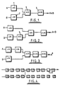
- FIG. 1 the mathematical operation of multiplication of two operands A and B is represented.
- Each of the operands is input to a respective cell 1 and 2 which converts the analogue value appearing at its input to an analogue output representing the logarithm of that value.
- a cell 3 then adds the two logarithms and a cell 4 converts the resultant logarithm to an analogue value representing the product of the analogue values represented by the operands A and B.
- Fig. 2 represents the mathematical operation of division. the cell 5 negating the analogue value at its input.
- Fig. 3 represents the operation of raising the operand A to the power B. It will be appreciated from Figs. 1, 2 and 3 that many simple and more complex mathematical operations can be performed by an appropriate network of functional cells each of which is in itself a relatively simple circuit.
- Fig. 4 represents a device in accordance with the present invention incorporating twenty cells arranged in two rows of ten cells each. Adjacent cells in each row are directly interconnected and the output of any one cell in each row may be connected to a second input of a respective cell in the other row by appropriate switching devices (not shown).
- Each cell may be switched to any one of eight conditions, that is non-inverting pass (NIP) in which the cell operates as a unity gain buffer stage, add in which the cell operates to add signals applied to two inputs, negate in which the cell changes the sign of the input signal, log in which the cell produces an output representing the logarithm of the input, alog in which the cell produces an output representing the anti-logarithm of its input, rectify (RECT) in which the cell produces an output corresponding to the rectification of the input, and auxiliary (AUX) which facilitates the connection of external components to perform extra functions such as integrate, differentiate or the like.
- NIP non-inverting pass
- Fig. 4 have been switched to a configuration in which they perform the function represented by Fig. 1. It will be noted that in this simple configuration many of the cells are acting merely as buffers or are dormant. The cells could be configured, however, to perform complex analogue functions.
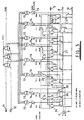
- Fig. 5 is a circuit diagram illustrating the circuit of one of the twenty cells shown in Fig. 4.
- Input signals representing operands are applied to input terminals 6 and 7.
- the two signals to be added would be applied to inputs 6 and 7.
- the input signals to be operated upon would be applied to input 6.
- the cell output appears at output terminal 8.
- the cell is powered from terminals 9 and 10 which carry respectively plus 2.5 volts and minus 2.5 volts.
- the cell is controlled by a digital data input applied to terminal 11 and a clock signal applied to terminal 12.
- the cell of Fig. 5 comprises seven subcells and an output circuit, these eight circuits being represented, respectively, in Figs. 6 to 13. Each of these circuits is controlled by the output of a respective nand gate 13 and associated inverter 14, the nand gates 13 being switched such that the output of each of them is high only when the three-bit output of an array of three flip-flops corresponds to a respective one of the eight possible values for such a three-bit output.
- the binary values are represented in Fig. 5 by 100, 110, 011, etc.
- each of the subcells can be controlled by the application of appropriate digital control signals to terminal 11.
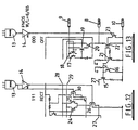
- the output circuit of Fig. 13 comprises an input bias circuit defined primarily by transistors 15 and 16, and an output stage defined primarily by transistor 17 to 23.
- Each of the subcells of Figs. 6 to 12 comprises a differential pair of transistors 24, 25 connected by series transistor switches 26 to a line 27 coupled to the collector of the transistor 15.
- Each of the transistor pairs 24 and 25 is also connected by lines 28, 29 to transistors 17, 18 and 19.
- the switches 26 are controlled by the outputs of respective inverters 14. Thus the switches 26 are normally off with the exception of the one switch associated with the nand gate 13 selected by the output of the digital control circuit.
- the provision of the series switch 26 may be sufficient when that switch is rendered non-conductive to prevent the existence of the circuit associated with that switch from significantly affecting the performance of the circuit as a whole.
- a subcell incorporates resistive components, however, it is desirable to provide auxiliary switches to minimise the shunt effect of those resistors.
- the log function subcell (Fig. 7) incorporates a shunt switch 30 controlled by the output of the respective nand gate 13. Shunt switches 30 are also provided in the add function subcell (Fig. 8), the negate subcell (Fig. 9), the alog subcell (Fig. 10) and the rectify subcell (Fig. 12).
- the nth cell 31 has an input terminal 32 extending across its full width and an output terminal 33, also extending across its full width.
- the nth cell is stacked immediately above the (n+1)th cell 34 which has input terminal 35 and output terminal 36.
- the conductive tracks 33 and 35 are connected together, minimising cell to cell attenuation given the large width of the tracks and the short length of the tracks.
- cell function selection is achieved using the series switches 26 to control current into the associated differential pairs 24, 25 and the shunt switches 32 to shunt resistive components associated with the differential pairs.
- the subcell responsible for that function is enabled by rendering the shunt switch 30 non-conductive to thereby release its associated resistor and rendering the series switch 26 conductive.
- This arrangement works well in terms of isolating the unused subcells. but there is a disadvantage in that current shunted to ground through the shunt switches 30 of the subcells which are not in use represents an unwanted use of power. This disadvantage can be overcome by introducing an isolation switch in series with the subcell resistors.
- the illustrated circuit components define log, add, negate, alog and rectify subcells. Each of these subcells incorporates a differential pair of transistors 24, 25 and a series transistor 26. Additional isolating switches 37 and 38 are provided, the isolating switches being rendered conductive only when the series switch 26 of the associated subcell is rendered conductive.
- the resistances of the isolating switches 37, 38 are not directly compensated given the illustrated circuit, but these resistances cancel when the log and alog functions are combined.
- isolating switches 38, 39 can cause problems due to capacitive feed through. This is avoided in the circuit of Fig. 15 by the provision of shunt switches 39 which are connected between the two isolating switches.
Landscapes
- Engineering & Computer Science (AREA)
- Computer Hardware Design (AREA)
- Physics & Mathematics (AREA)
- Theoretical Computer Science (AREA)
- Mathematical Physics (AREA)
- General Physics & Mathematics (AREA)
- Design And Manufacture Of Integrated Circuits (AREA)
- Electronic Switches (AREA)
- Analogue/Digital Conversion (AREA)
Claims (6)
- Programmierbare Analogeinrichtung, umfassend ein Feld von Zellen, die jeweils steuerbar sind, um irgendeine eines vorgegebenen Satzes von Analogfunktionen auszuführen, und eine Einrichtung zum selektiven Verbinden der Zellen untereinander, um eine Analogschaltung zwischen einem Einrichtungseingang und einem Einrichtungsausgang zu definieren, dadurch gekennzeichnet, dass jede Zelle ein Feld von Subzellen umfasst, wobei jede dafür ausgelegt ist, um eine jeweilige des vorgegebenen Satzes von Analogfunktionen auszuführen, wobei jede Zelle eine Eingangsvorpolungsschaltung umfasst, wobei jede Subzelle einen Reihenschalter umfasst, der selektiv auf einen Leitungszustand geschaltet werden kann, um so die Subzelle mit der Eingangsvorpolungsschaltung zu verbinden, wobei jede Zelle eine Funktionssteuerschaltung umfasst, die selektiv auf einen der Reihenschalter in Abhängigkeit von einem Funktionswähleingang schaltet, wobei jede Subzelle ein differentielles Paar von Transistoren umfasst, die dann, wenn sie von dem jeweiligen Reihenschalter mit der Vorpolungsschaltung elektrisch gekoppelt sind, einen Operationsverstärker mit der Eingangsvorpolungsschaltung definieren, und jede Zelle eine Ausgangsschaltung umfasst, die mit jeder der Subzellen verbunden ist, so dass die Ausgangsschaltung einen Analogausgang in Abhängigkeit von der Funktion des Operationsverstärkers, der von der Eingangsvorpolungsschaltung und dem differentiellen Transistorpaar, mit dem die Eingangsvorpolungsschaltung über den leitenden Reihenschalter verbunden ist, definiert ist, liefert.
- Einrichtung nach Anspruch 1, ferner umfassend Schalter, wobei jeder einen Teil einer jeweiligen Subzelle bildet und von der Funktionssteuerschaltung gesteuert wird, um nur dann in einen nicht-leitenden Zustand gebracht zu werden, wenn der Reihenschalter der jeweiligen Subzelle leitend ist, wobei die weiteren Schalter angeordnet sind, wenn leitend, um den Effekt der zugehörigen Subzelle bei dem Betrieb der Einrichtung zu minimieren.
- Einrichtung nach Anspruch 2, wobei die weiteren Schalter mit Nebenschluss-Widerstandskomponenten der zugehörigen Subzellen verbunden sind.
- Einrichtung nach Anspruch 1, wobei das differentielle Paar von Transistoren von wenigstens einer Subzelle zu wenigstens einer Widerstandskomponente gehört, und ein isolierender Schalter in Reihe zwischen die Widerstandskomponente und das differentielle Paar von Transistoren geschaltet ist, wobei der isolierende Schalter nur dann leitend gemacht wird, wenn der Reihenschalter der Subzelle leitend gemacht wird.
- Einrichtung nach Anspruch 4, wobei das differentielle Paar von Transistoren mit Quellen- und Rückkopplungswiderständen über jeweilige isolierende Schalter gekoppelt ist.
- Einrichtung nach Anspruch 5, wobei ein Nebenschluss-Schalter zwischen die zwei isolierenden Schalter geschaltet ist.
Applications Claiming Priority (3)
| Application Number | Priority Date | Filing Date | Title |
|---|---|---|---|
| GBGB9618648.1A GB9618648D0 (en) | 1996-09-06 | 1996-09-06 | Field programmable analogue processor |
| GB9618648 | 1996-09-06 | ||
| PCT/GB1997/002336 WO1998010362A1 (en) | 1996-09-06 | 1997-09-01 | Field programmable analogue processor |
Publications (2)
| Publication Number | Publication Date |
|---|---|
| EP0925545A1 EP0925545A1 (de) | 1999-06-30 |
| EP0925545B1 true EP0925545B1 (de) | 2002-06-12 |
Family
ID=10799541
Family Applications (1)
| Application Number | Title | Priority Date | Filing Date |
|---|---|---|---|
| EP97936819A Expired - Lifetime EP0925545B1 (de) | 1996-09-06 | 1997-09-01 | Benutzerprogrammierbarer analogprozessor |
Country Status (6)
| Country | Link |
|---|---|
| US (1) | US6415429B1 (de) |
| EP (1) | EP0925545B1 (de) |
| AU (1) | AU3951397A (de) |
| DE (1) | DE69713349T2 (de) |
| GB (1) | GB9618648D0 (de) |
| WO (1) | WO1998010362A1 (de) |
Families Citing this family (3)
| Publication number | Priority date | Publication date | Assignee | Title |
|---|---|---|---|---|
| GB2377568B (en) | 2001-07-12 | 2004-12-15 | Fast Analog Solutions Ltd | Low pass filter |
| FI116254B (fi) * | 2003-11-14 | 2005-10-14 | Nokia Corp | Signaalien suodatus |
| US9582687B2 (en) | 2015-05-15 | 2017-02-28 | King Fahd University Of Petroleum And Minerals | Reconfigurable integrator/differentiator circuit using current follower based simulated inductor |
Family Cites Families (5)
| Publication number | Priority date | Publication date | Assignee | Title |
|---|---|---|---|---|
| GB9007492D0 (en) | 1990-04-03 | 1990-05-30 | Pilkington Micro Electronics | Semiconductor integrated circuit |
| WO1995017781A1 (en) * | 1993-12-23 | 1995-06-29 | The State Of Oregon, Acting By And Through The State Board Of Higher Education On Behalf Of Portland State University | Programmable analog array circuit |
| US5563526A (en) * | 1994-01-03 | 1996-10-08 | Texas Instruments Incorporated | Programmable mixed-mode integrated circuit architecture |
| US5541538A (en) * | 1994-09-01 | 1996-07-30 | Harris Corporation | High speed comparator |
| US6121823A (en) * | 1999-03-17 | 2000-09-19 | Analytical Technology, Inc. | Electrical circuit for sensors requiring a variety of bias voltages |
-
1996
- 1996-09-06 GB GBGB9618648.1A patent/GB9618648D0/en active Pending
-
1997
- 1997-09-01 AU AU39513/97A patent/AU3951397A/en not_active Abandoned
- 1997-09-01 WO PCT/GB1997/002336 patent/WO1998010362A1/en not_active Ceased
- 1997-09-01 EP EP97936819A patent/EP0925545B1/de not_active Expired - Lifetime
- 1997-09-01 DE DE69713349T patent/DE69713349T2/de not_active Expired - Fee Related
- 1997-09-01 US US09/254,490 patent/US6415429B1/en not_active Expired - Fee Related
Also Published As
| Publication number | Publication date |
|---|---|
| GB9618648D0 (en) | 1996-10-16 |
| WO1998010362A1 (en) | 1998-03-12 |
| DE69713349D1 (de) | 2002-07-18 |
| US6415429B1 (en) | 2002-07-02 |
| DE69713349T2 (de) | 2003-02-20 |
| AU3951397A (en) | 1998-03-26 |
| EP0925545A1 (de) | 1999-06-30 |
Similar Documents
| Publication | Publication Date | Title |
|---|---|---|
| Vittoz | Future of analog in the VLSI environment | |
| US4233524A (en) | Multi-function logic circuit | |
| EP0456399A2 (de) | Logisches Modul mit konfigurierbaren kombinatorischen und sequentiellen Blöcken | |
| JPH0660139A (ja) | Mosトランジスタの論理機能ブロックの消費電力計算装置 | |
| JPH0786921A (ja) | 現場プログラム可能なディジタル信号処理アレイ集積回路 | |
| US4749886A (en) | Reduced parallel EXCLUSIVE or and EXCLUSIVE NOR gate | |
| US5664211A (en) | Null convention threshold gate | |
| EP0123222B1 (de) | Digitalanalogwandler | |
| US4914614A (en) | Multivalued ALU | |
| US5977663A (en) | Dynamic threshold gates with embedded registration | |
| EP0925545B1 (de) | Benutzerprogrammierbarer analogprozessor | |
| Schlottmann et al. | A mite-based translinear FPAA | |
| KR19990022761A (ko) | 제 1 뉴런 mosfet 및 기준 소오스에 의해 제공되는 2개의 전기값을 비교하기 위한 회로 | |
| Siskos et al. | Analog implementation of fast min/max filtering | |
| US3016466A (en) | Logical circuit | |
| US5514982A (en) | Low noise logic family | |
| Twigg et al. | Configurable analog signal processing | |
| US5491431A (en) | Logic module core cell for gate arrays | |
| US5894426A (en) | Maximum/minimum value determination apparatus | |
| US6338157B1 (en) | Threshold element and method of designing the same | |
| Quintáns et al. | A virtual instrumentation laboratory based on a reconfigurable coprocessor | |
| US5448506A (en) | Multiplication operational circuit device | |
| JPH0479516A (ja) | 集積回路装置における遅延回路 | |
| Halonen et al. | Programmable analog VLSI CNN chip with local digital logic | |
| US5999643A (en) | Switched-current type of hamming neural network system for pattern recognition |
Legal Events
| Date | Code | Title | Description |
|---|---|---|---|
| PUAI | Public reference made under article 153(3) epc to a published international application that has entered the european phase |
Free format text: ORIGINAL CODE: 0009012 |
|
| 17P | Request for examination filed |
Effective date: 19990331 |
|
| AK | Designated contracting states |
Kind code of ref document: A1 Designated state(s): DE ES FR GB IT |
|
| 17Q | First examination report despatched |
Effective date: 19991007 |
|
| GRAG | Despatch of communication of intention to grant |
Free format text: ORIGINAL CODE: EPIDOS AGRA |
|
| GRAG | Despatch of communication of intention to grant |
Free format text: ORIGINAL CODE: EPIDOS AGRA |
|
| GRAH | Despatch of communication of intention to grant a patent |
Free format text: ORIGINAL CODE: EPIDOS IGRA |
|
| GRAH | Despatch of communication of intention to grant a patent |
Free format text: ORIGINAL CODE: EPIDOS IGRA |
|
| GRAA | (expected) grant |
Free format text: ORIGINAL CODE: 0009210 |
|
| AK | Designated contracting states |
Kind code of ref document: B1 Designated state(s): DE ES FR GB IT |
|
| PG25 | Lapsed in a contracting state [announced via postgrant information from national office to epo] |
Ref country code: IT Free format text: LAPSE BECAUSE OF FAILURE TO SUBMIT A TRANSLATION OF THE DESCRIPTION OR TO PAY THE FEE WITHIN THE PRESCRIBED TIME-LIMIT;WARNING: LAPSES OF ITALIAN PATENTS WITH EFFECTIVE DATE BEFORE 2007 MAY HAVE OCCURRED AT ANY TIME BEFORE 2007. THE CORRECT EFFECTIVE DATE MAY BE DIFFERENT FROM THE ONE RECORDED. Effective date: 20020612 Ref country code: FR Free format text: LAPSE BECAUSE OF FAILURE TO SUBMIT A TRANSLATION OF THE DESCRIPTION OR TO PAY THE FEE WITHIN THE PRESCRIBED TIME-LIMIT Effective date: 20020612 |
|
| REG | Reference to a national code |
Ref country code: GB Ref legal event code: FG4D |
|
| REF | Corresponds to: |
Ref document number: 69713349 Country of ref document: DE Date of ref document: 20020718 |
|
| PGFP | Annual fee paid to national office [announced via postgrant information from national office to epo] |
Ref country code: FR Payment date: 20020910 Year of fee payment: 6 |
|
| PG25 | Lapsed in a contracting state [announced via postgrant information from national office to epo] |
Ref country code: ES Free format text: LAPSE BECAUSE OF FAILURE TO SUBMIT A TRANSLATION OF THE DESCRIPTION OR TO PAY THE FEE WITHIN THE PRESCRIBED TIME-LIMIT Effective date: 20021220 |
|
| EN | Fr: translation not filed | ||
| PLBE | No opposition filed within time limit |
Free format text: ORIGINAL CODE: 0009261 |
|
| STAA | Information on the status of an ep patent application or granted ep patent |
Free format text: STATUS: NO OPPOSITION FILED WITHIN TIME LIMIT |
|
| 26N | No opposition filed |
Effective date: 20030313 |
|
| PGFP | Annual fee paid to national office [announced via postgrant information from national office to epo] |
Ref country code: DE Payment date: 20050825 Year of fee payment: 9 |
|
| PGFP | Annual fee paid to national office [announced via postgrant information from national office to epo] |
Ref country code: GB Payment date: 20050831 Year of fee payment: 9 |
|
| PG25 | Lapsed in a contracting state [announced via postgrant information from national office to epo] |
Ref country code: DE Free format text: LAPSE BECAUSE OF NON-PAYMENT OF DUE FEES Effective date: 20070403 |
|
| GBPC | Gb: european patent ceased through non-payment of renewal fee |
Effective date: 20060901 |
|
| PG25 | Lapsed in a contracting state [announced via postgrant information from national office to epo] |
Ref country code: GB Free format text: LAPSE BECAUSE OF NON-PAYMENT OF DUE FEES Effective date: 20060901 |