EP0923799B1 - Frequency doubled laser with an intracavity nonlinear, quasi-phase matching element - Google Patents
Frequency doubled laser with an intracavity nonlinear, quasi-phase matching element Download PDFInfo
- Publication number
- EP0923799B1 EP0923799B1 EP97939284A EP97939284A EP0923799B1 EP 0923799 B1 EP0923799 B1 EP 0923799B1 EP 97939284 A EP97939284 A EP 97939284A EP 97939284 A EP97939284 A EP 97939284A EP 0923799 B1 EP0923799 B1 EP 0923799B1
- Authority
- EP
- European Patent Office
- Prior art keywords
- laser
- microchip
- radiation
- cavity
- phase matching
- Prior art date
- Legal status (The legal status is an assumption and is not a legal conclusion. Google has not performed a legal analysis and makes no representation as to the accuracy of the status listed.)
- Expired - Lifetime
Links
Images


Classifications
-
- H—ELECTRICITY
- H01—ELECTRIC ELEMENTS
- H01S—DEVICES USING THE PROCESS OF LIGHT AMPLIFICATION BY STIMULATED EMISSION OF RADIATION [LASER] TO AMPLIFY OR GENERATE LIGHT; DEVICES USING STIMULATED EMISSION OF ELECTROMAGNETIC RADIATION IN WAVE RANGES OTHER THAN OPTICAL
- H01S3/00—Lasers, i.e. devices using stimulated emission of electromagnetic radiation in the infrared, visible or ultraviolet wave range
- H01S3/05—Construction or shape of optical resonators; Accommodation of active medium therein; Shape of active medium
- H01S3/06—Construction or shape of active medium
- H01S3/0627—Construction or shape of active medium the resonator being monolithic, e.g. microlaser
-
- H—ELECTRICITY
- H01—ELECTRIC ELEMENTS
- H01S—DEVICES USING THE PROCESS OF LIGHT AMPLIFICATION BY STIMULATED EMISSION OF RADIATION [LASER] TO AMPLIFY OR GENERATE LIGHT; DEVICES USING STIMULATED EMISSION OF ELECTROMAGNETIC RADIATION IN WAVE RANGES OTHER THAN OPTICAL
- H01S3/00—Lasers, i.e. devices using stimulated emission of electromagnetic radiation in the infrared, visible or ultraviolet wave range
- H01S3/10—Controlling the intensity, frequency, phase, polarisation or direction of the emitted radiation, e.g. switching, gating, modulating or demodulating
- H01S3/106—Controlling the intensity, frequency, phase, polarisation or direction of the emitted radiation, e.g. switching, gating, modulating or demodulating by controlling devices placed within the cavity
- H01S3/108—Controlling the intensity, frequency, phase, polarisation or direction of the emitted radiation, e.g. switching, gating, modulating or demodulating by controlling devices placed within the cavity using non-linear optical devices, e.g. exhibiting Brillouin or Raman scattering
- H01S3/109—Frequency multiplication, e.g. harmonic generation
-
- G—PHYSICS
- G02—OPTICS
- G02F—OPTICAL DEVICES OR ARRANGEMENTS FOR THE CONTROL OF LIGHT BY MODIFICATION OF THE OPTICAL PROPERTIES OF THE MEDIA OF THE ELEMENTS INVOLVED THEREIN; NON-LINEAR OPTICS; FREQUENCY-CHANGING OF LIGHT; OPTICAL LOGIC ELEMENTS; OPTICAL ANALOGUE/DIGITAL CONVERTERS
- G02F1/00—Devices or arrangements for the control of the intensity, colour, phase, polarisation or direction of light arriving from an independent light source, e.g. switching, gating or modulating; Non-linear optics
- G02F1/35—Non-linear optics
- G02F1/353—Frequency conversion, i.e. wherein a light beam is generated with frequency components different from those of the incident light beams
- G02F1/3544—Particular phase matching techniques
- G02F1/3548—Quasi phase matching [QPM], e.g. using a periodic domain inverted structure
-
- H—ELECTRICITY
- H01—ELECTRIC ELEMENTS
- H01S—DEVICES USING THE PROCESS OF LIGHT AMPLIFICATION BY STIMULATED EMISSION OF RADIATION [LASER] TO AMPLIFY OR GENERATE LIGHT; DEVICES USING STIMULATED EMISSION OF ELECTROMAGNETIC RADIATION IN WAVE RANGES OTHER THAN OPTICAL
- H01S3/00—Lasers, i.e. devices using stimulated emission of electromagnetic radiation in the infrared, visible or ultraviolet wave range
- H01S3/05—Construction or shape of optical resonators; Accommodation of active medium therein; Shape of active medium
- H01S3/06—Construction or shape of active medium
- H01S3/0602—Crystal lasers or glass lasers
- H01S3/0604—Crystal lasers or glass lasers in the form of a plate or disc
-
- H—ELECTRICITY
- H01—ELECTRIC ELEMENTS
- H01S—DEVICES USING THE PROCESS OF LIGHT AMPLIFICATION BY STIMULATED EMISSION OF RADIATION [LASER] TO AMPLIFY OR GENERATE LIGHT; DEVICES USING STIMULATED EMISSION OF ELECTROMAGNETIC RADIATION IN WAVE RANGES OTHER THAN OPTICAL
- H01S3/00—Lasers, i.e. devices using stimulated emission of electromagnetic radiation in the infrared, visible or ultraviolet wave range
- H01S3/05—Construction or shape of optical resonators; Accommodation of active medium therein; Shape of active medium
- H01S3/06—Construction or shape of active medium
- H01S3/0602—Crystal lasers or glass lasers
- H01S3/0615—Shape of end-face
-
- H—ELECTRICITY
- H01—ELECTRIC ELEMENTS
- H01S—DEVICES USING THE PROCESS OF LIGHT AMPLIFICATION BY STIMULATED EMISSION OF RADIATION [LASER] TO AMPLIFY OR GENERATE LIGHT; DEVICES USING STIMULATED EMISSION OF ELECTROMAGNETIC RADIATION IN WAVE RANGES OTHER THAN OPTICAL
- H01S3/00—Lasers, i.e. devices using stimulated emission of electromagnetic radiation in the infrared, visible or ultraviolet wave range
- H01S3/05—Construction or shape of optical resonators; Accommodation of active medium therein; Shape of active medium
- H01S3/08—Construction or shape of optical resonators or components thereof
- H01S3/08018—Mode suppression
- H01S3/08022—Longitudinal modes
- H01S3/08031—Single-mode emission
- H01S3/08036—Single-mode emission using intracavity dispersive, polarising or birefringent elements
-
- H—ELECTRICITY
- H01—ELECTRIC ELEMENTS
- H01S—DEVICES USING THE PROCESS OF LIGHT AMPLIFICATION BY STIMULATED EMISSION OF RADIATION [LASER] TO AMPLIFY OR GENERATE LIGHT; DEVICES USING STIMULATED EMISSION OF ELECTROMAGNETIC RADIATION IN WAVE RANGES OTHER THAN OPTICAL
- H01S3/00—Lasers, i.e. devices using stimulated emission of electromagnetic radiation in the infrared, visible or ultraviolet wave range
- H01S3/05—Construction or shape of optical resonators; Accommodation of active medium therein; Shape of active medium
- H01S3/08—Construction or shape of optical resonators or components thereof
- H01S3/081—Construction or shape of optical resonators or components thereof comprising three or more reflectors
- H01S3/0813—Configuration of resonator
- H01S3/0815—Configuration of resonator having 3 reflectors, e.g. V-shaped resonators
-
- H—ELECTRICITY
- H01—ELECTRIC ELEMENTS
- H01S—DEVICES USING THE PROCESS OF LIGHT AMPLIFICATION BY STIMULATED EMISSION OF RADIATION [LASER] TO AMPLIFY OR GENERATE LIGHT; DEVICES USING STIMULATED EMISSION OF ELECTROMAGNETIC RADIATION IN WAVE RANGES OTHER THAN OPTICAL
- H01S3/00—Lasers, i.e. devices using stimulated emission of electromagnetic radiation in the infrared, visible or ultraviolet wave range
- H01S3/10—Controlling the intensity, frequency, phase, polarisation or direction of the emitted radiation, e.g. switching, gating, modulating or demodulating
- H01S3/11—Mode locking; Q-switching; Other giant-pulse techniques, e.g. cavity dumping
- H01S3/1123—Q-switching
- H01S3/113—Q-switching using intracavity saturable absorbers
Definitions
- the present invention refers to a method for generating laser radiation, comprising the steps of generating laser radiation of a fundamental wavelength from a laser microchip in a laser cavity by pumping it with radiation from a diode laser.
- the present invention also refers to a laser comprising: first and second reflecting elements defining a laser cavity; and a laser microchip provided in said laser cavity and arranged to be pumped by radiation from a diode laser to thereby generate laser radiation of a fundamental wavelength.
- Microchip lasers and miniature lasers that uses laser microchip are small, robust, compact, diode pumped solid state lasers which can be manufactured in large quantities at a low cost.
- advantages and interesting application areas of microchip lasers reference is given to the article "Microchip Lasers and Laser Arrays: Technology and Applications", Optics and Photonics News, Nov. 1995, pp. 16-19.
- Examples on interesting application areas for microchip lasers include transmission of cable TV signals, image generation, material treatment, etc.
- the microchip laser concept was developed at the MIT Lincoln Laboratory in the middle of the 1980's and aims to use semiconductor packaging and fabrication technology for manufacturing of lasers.
- Simple microchip lasers are made from a rod of laser material, normally a crystal or a glass, such as Nd:YAG.
- the rod is cut into wafers which are polished to show planar and parallel surfaces which is then coated with dielectric mirrors, usually by some kind of vacuum deposition technology.
- the wafers are then cut into chips using conventional semiconductor cutting technology.
- Laser crystal chips usually have an area of approximately 1x1 to 4x4 mm 2 and a thickness in the radiation direction of less than 4 mm.
- the microchip laser technology thus provides for mass production of laser microchips. For example, more than 2,000 chips can be fabricated from a 2.5 cm (1 inch) long Nd:YAG rod.
- different types of functional elements such as Q-switches or frequency doubling elements etc.
- Q-switches or frequency doubling elements etc. can be integrated in the laser cavity as disclosed in T. TAIRA et al., "Intracavity Frequency doubling und Q-switching in diode-laser-pumped Nd : yvon lasers", Applied Optics, 34(21), 4298 (1995).
- the laser chip and one or more functional elements may be brought together and contacted through thermal diffusion bonding or similar.
- the different elements are mounted together in this way, and mirrors are applied directly on the chips/elements, the appearance of air gaps is eliminated in the laser cavity, which eliminates risk for reflections which may disturb the lasing.
- laser microchips can also be used in so called miniature lasers, in which the laser microchip and other incorporated functional elements are not necessarily arranged in contact with each other but instead are separated from each other by small gaps.
- the laser material is doped with ions of a rare earth metal that provides the lasing.
- the laser radiation can only be.built up over a relatively short distance.
- the laser microchip material is given a high degree of dopant as compared to other solid state lasers.
- the doping provides for more than 0.1 percent by weight of the laser material, while the degree of dopant in a conventional solid states laser usually is far below 1,000 ppm, for example 50 ppm for a 10 cm long laser crystal.
- the high degree of dopant in the laser microchip provides a short absorption length, which among other things makes it possible to store a large amount of energy in a small volume, but also leads to a shorter lifetime for electrons excited to the meta stable upper laser level.
- neodymium Nd
- Er erbium
- Pr prasodymium
- Ho holmium
- Yb ytterbium
- YAG - Yttrium Aluminium Garnet (Y 3 Al 5 O 12 ) and yttrium vanadate (YVO 4 ) are two of the most commonly used crystals today.
- YAG has a comparatively long lifetime for the metastable state, but a lower absorption cross-section (i.e. a lower absorption capacity) than yttrium vanadate, which enables the latter to be made shorter.
- Many other crystals may be used, such as YLF (yttrium-lithium-floride), LNP, LSB, SVAP, and GdVO 4 (gadolinium vanadate).
- YLF yttrium-lithium-floride
- Nd lasers are used at the strong transition 4 F 3/2 ⁇ 4 I 11/2 . This provides lasing at wavelengths slightly longer than 1 ⁇ m, somewhat varying as dependent on the host material. For Nd:YAG this wavelength usually appears at 1064 nm.
- Other interesting transitions that may be used are 4 F 3/2 ⁇ 4 I 9/2 , which gives lasing at shorter wavelengths (946 nm for Nd:YAG), and 4 F 3/2 ⁇ 4 I 13/2 , which gives lasing at a longer wavelength (1360 nm for Nd:YAG).
- the laser microchip is usually pumped by a diode laser that gives a wavelength matched to the absorption band of the used rare earth metal.
- the pumped laser may be single mode or multimode.
- the function of the diode laser is only to excite electrons in a small volume of the laser microchip and thereby transfer the largest possible amount of energy to the mode of the laser microchip.
- a relatively cheap diode laser is thus preferably used, as the laser microchip will transfer the relatively poor spectral and spatial properties of the diode laser output into a laser beam having pure spectral and spatial properties and low noise.
- microchip lasers are characterized by a tendency to lase in single mode, which is desired in many applications.
- dn/dT the change in refractive index with temperature
- the thermal expansion of the material also contributes to the creation of this lens.
- the lens stabilizes the laser cavity, which would otherwise have been an unstable (coplanar) cavity.
- a stable resonator may be formed if the pump light is concentrated. This phenomenon gives an automatically stabilized resonator, which enables simple manufacturing and alignment.
- a very important type of microchip lasers and miniature lasers which utilizes laser microchips are such that uses so called intra-cavity frequency doubling.
- These types of lasers comprise an intra-cavity arranged functional element in the form of a frequency doubling crystal that provides frequency doubling (SHG - second harmonic generation) of the fundamental light wave, i.e. which converts the laser radiation of the fundamental wavelength from the laser microchip into laser radiation of half the fundamental wavelength. Examples on such intra-cavity frequency doubling in a microchip laser has been described in the international patent application WO 90/09688.
- Intra-cavity frequency doubled microchip lasers can show a very high conversion efficiency even at low pump power. This is caused by the laser mode being concentrated, i.e. has a high intensity, in the short microchip laser cavity, and by the laser mirrors being made high reflecting at the laser wavelength, which means that the fundamental light wave is confined between the mirrors to build up a high intensity.
- phase matching is required, which means that the polarization induced at different places in the material emit frequency doubled radiation coherently. This require that the two waves ⁇ and 2 ⁇ perceive the same refractive indices. This is normally not possible, as the dispersion makes the refractive index at the shorter wavelength larger than the refractive index at the longer wavelength.
- phase matching When using intra-cavity frequency doubling in microchip lasers, so-called birefringent phase matching is utilized.
- a difference in refractive index for different polarization in uniaxial and biaxial non-linear crystals is utilized.
- the difference in refractive index makes it possible to achieve the desired phase matching.
- Birefringent phase matching is used since birefringent crystal chips may be mass produced in a similar way as the laser chips mentioned above.
- a KTP crystal rod can be cut into wafers along those planes that are required to provide a crystal having the necessary double refraction for birefringent phase matching in different directions. These wafers can then be cut into chips that can be bonded to the laser chips by pick and place technology, as discussed above.
- Another disadvantage is that the polarization of the light is rotated when the light is propagating through a birefringent crystal. This means that light that has propagated one round-trip through the cavity does not have the same state of polarization as it had when it started. This means that the length of the crystal has to be controlled very accurately to avoid such stochastic variations, which otherwise would have severe effect on the frequency doubled output. Each separate crystal has to be polished to an exact length. Further problems occur when the temperature changes, as the refractive indices and thereby the optical path length changes with temperature, which will lead to the fluctuation in the state of polarization. For example, a stable operation for a temperature interval From 10 to 70 °C would be very hard to achieve. To the best knowledge of the inventors, this problem has not been solved yet, which has impeded the realization of temperature stable frequency doubled microchip lasers.
- An object of the invention is thus to realize frequency doubling in a laser having a laser microchip in such a manner that the laser shows a stable state of polarization, a high efficiency and can be fabricated at a low price.
- a method of the kind mentioned in the introduction characterized by the step of converting said laser radiation of said fundamental wavelength, by means of intra-cavity quasi-phase matching in said laser cavity, into frequency doubled radiation having a wavelength being half as long as the fundamental wavelength.
- a laser of the kind mentioned in the introduction characterized by an optical non-linear, quasi-phase matching element provided in the laser cavity to receive said laser radiation of the fundamental wavelength from said laser microchip and to emit frequency doubled laser radiation of a wavelength being half as long as said fundamental wavelength.
- frequency doubling is achieved in connection with the use of a laser micro chip by so called quasi-phase matching.
- the distance l c is usually called the coherence length.
- the coherence length In such a way, light generated in the second region will be in phase with the light generated over the first region. After the next coherence length, the nonlinearity is inverted again. The nonlinearity is in this way modulated periodically throughout the material.
- Quasi-phase matching has several advantages. For example, any wavelength can be phase matched throughout the transparency region of the nonlinear medium by proper choice of the periodic modulation of the nonlinearity. Furthermore, a single polarization can be used, and it is thus no longer necessary to rely on birefringent crystals to get the desired phase matching. Furthermore, for many materials, the largest nonlinearty cannot be used for birefringent phase matching, but it can be used for quasi-phase matching. Theoretically, the efficiency in the frequency doubling process may be improved by a factor of ten or more for quasi-phase matching over conventional birefringent phase matching. Using quasi-phase matching, it is also relatively easy to achieve phase matching at shorter wavelengths.
- An interesting application is to use one single material and quasi-phase match the three laser lines for the Nd:YAG laser to blue, green and red light, what not would not have been possible with conventional birefringent phase matching.
- Small compact lasers at these wavelength are very interesting for many applications, particularly image formation and displays.
- the quasi-phase matching element consist of an optically nonlinear crystal whose c-axis is directed perpendicular to the propagation direction through the element.
- This is called noncritical phase matching and means that the fundamental wavelength beam and the frequency doubled wavelength beam are aligned. This carry a great advantage, since the beam quality is preserved.
- "walk-off" effects typically appear, i.e. the frequency doubled wave is propagating in a different direction than the fundamental, which results in an undesired elliptical beam.
- the conversion efficiency is proportional to the interaction length, which means that it is important to have the two waves to propagate overlapping the longest possible distance to get a maximum energy transferred to the frequency doubled wave.
- said optically nonlinear crystal is made of LiNbO 3 , LiTaO 3 , KTiOPO 4 , RbTiOPO 4 , RbTiAsO 4 , CsTiOAsO 4 , or KTiOAsO 4 .
- KTiOPO 4 (KTP) is the presently most commonly used material and can hence be obtained in good quality and at a low price.
- the polarization axis is inverted periodically. This is called ferroelectric domain inversion.
- Example on manners of achieving domain reversal in ferroelectric crystals are the diffusion at high temperatures, the ion-exchange and poling with electric fields. As mentioned above, the period should be chosen to compensate for phase velocity mismatch between the fundamental and the frequency doubled wave.
- a light converging element provided to converge said laser radiation of the first wavelength so that the light intensity, with respect to said laser radiation of the first wavelength, becomes as large as possible in said quasi-phase matching element.
- the light intensity in the quasi-phase matching element is increased, and as the conversion efficiency is increasing with increasing intensity, an increase in the output power, at the frequency doubled wavelength, is obtained from the quasi-phase matching element.
- converging is obtained by said first reflecting element having a both inward directed and curved reflecting surface, with respect to said laser cavity, forming said light converging element.
- the laser microchip is preferentially provided to have a correspondingly curved surface on which said reflecting element, forming the light converging element, is provided. This gives a very compact construction with high intensity in the quasi-phase matching element.
- a polarizer may be placed in the cavity to achieve linearly polarized laser emission and thereby eliminate polarization instabilities.
- a polarization discriminating element is provided in the laser cavity.
- said pulsing element is a passive Q-switch consisting of a saturable absorber preferably made in a Cr-doped crystal or a Cr-doped glass.
- the laser microchip generates a stable single-mode at a wavelength falling within the phase matching bandwidth of the quasi-phase matching element.
- a short cavity which is the consequence of a short microchip laser, normally gives single mode lasing, but the occurrence of an undesired multi-mode lasing can be eliminated by providing a mode discriminating element, which only allows lasing in desired modes, in the cavity.
- Pockel cells For active Q-switching, so called Pockel cells are utilized. This could for example be a crystal of KTP, LiNbO 3 or LiTaO 3 which is modulated by a voltage applied over electrodes applied on the surfaces of the crystal. Active control gives larger freedom in the design of the laser as well as for the temporal noise in the emission of pulses.
- Another preferred way to transfer the energy from the diode laser to the laser element is to use a holographic optical element.
- GRIN lens graded index lens
- said elements of different kinds are aligned to form an essentially straight beam path through the laser cavity.
- a straight coinciding beam path will provide a higher efficiency in the transfer of energy from the fundamental wave to the frequency doubled wave, as discussed above.
- the beam path essentially follows a straight line between the reflectors and that the planar surfaces of the different elements are arranged perpendicular to the beam path, i.e. the arrangement forms a so called planar cavity.
- a more or less folded beam path may also be an alternative for miniature lasers using microchips.
- both of the reflecting elements are provided to transmit said frequency doubled radiation out from the laser cavity. If only one of the reflecting elements transmits the frequency doubled radiation and the other reflecting element reflects the frequency doubled radiation, destructive interference might occur.
- the laser microchip consists of a material containing more than 0.1 weight percent of the laser dopant.
- the high degree of dopant is compensating the relatively short optical path length of the laser microchip.
- said laser microchip has a length in the optical path direction of less than 3 mm, preferably less than 1.5 mm.
- the dopant is neodymium or ytterbium and the host material is YAG or YVO 4 .
- said quasi-phase matching element preferably has a length in the beam path direction of less than 4 mm, preferably less than 2 mm.
- the cross-section area of the quasi-phase matching element is smaller than 10 mm 2 perpendicular to the beam propagation direction, preferably smaller than 5 mm 2 .
- the elements are arranged in contact with each other to form a cavity without any air gaps which might cause reflections.
- the laser microchip and the quasi-phase matching element are mounted together by thermal diffusion and that the reflecting element is applied on the outside of the laser microchip and the quasi-phase matching element,. respectively, by vacuum evaporation.
- a simpler technique for mounting, which can be applicable in some cases, is to simply glue two or more elements together.
- one or more of said elements are provided on a carrier where they form the miniature or microchip laser. It is furthermore understood that fine adjustments of the elements with respect to each other is possible if they are provided separate from each other on the carrier. If they are mounted separately, internal reflection may be avoided by coating the individual components with anti-reflection coatings.
- the quasi-phase matching element comprises several quasi-phase matching gratings provided in parallel with slightly different grating periods.
- the element may be provided with slightly different grating periods in different parts of the element.
- coupling of the diode laser light may be optimized so that the frequency doubling takes place at a grating period giving the highest frequency doubling efficiency.
- a crystal having different grating periods can also be made by forming the periodic domain inversions of the crystal in a fan-like diverging form, as will be described below.
- the pumping of the laser microchip can be achieved in several ways.
- the pumping diode laser can be provided close to the laser microchip, whereby the pumping is provided directly from the diode laser to the laser microchip.
- This construction gives a very compact device, but unfortunately the risk of causing damage on the optical surfaces during construction of the laser, as the diode laser has to be provided only a few micrometers away from the laser microchip.
- Another method is to transfer the laser light from the diode laser to the laser microchip through an optical fiber.
- This method shows the advantages that the diode laser can be cooled independently of the microchip, as it can be placed away from the chip, that a large amount of light is provided to the laser microchip, as the fibre makes sure that the divergence of light from the diode laser is limited, and that the coupling of light to the laser microchip can be adjusted during production for optimizing thereof, which facilitates mass production.
- the optical fibre coupling is replaced by one or several lenses, or other types of optics, which however can be less desired for mass production as this usually requires extensive adjustments and optimizations.
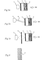
- the microchip laser comprises an approximately 1 mm long laser microchip 1 which is made of a solid-state laser of Nd:YAG.
- the laser microchip 1 is pumped with optical energy from a diode laser 7 and emits a fundamental wavelength.
- an approximately 1 mm long optically nonlinear crystal 2 of KTP is arranged in contact with the laser microchip 1.
- the elements 1 and 2 are mounted together by diffusion bonding and reflecting element 3 and 4 are provided on the end surfaces of the elements 1 and 2 to form an approximately 2 mm long laser cavity which consequently comprises both the laser chip 1 and the quasi-phase matching crystal 2.
- the optical nonlinear crystal 2 comprises a quasi-phase matching grating with a quasi-phase matching bandwidth matched to the fundamental laser wavelength from the laser chip 1.
- the c-axes of the crystal is directed perpendicularly to the beam path through the crystal, i.e. perpendicularly to direction of the arrow SH.
- the crystal 2 receives the fundamental light wave from the laser chip 1 and transform it into a frequency doubled light wave SH.
- the reflecting elements 3 and 4 reflect essentially all the fundamental radiation and transmits as much as possible of the frequency doubled light.
- a frequency doubled microchip laser according to a second embodiment of the invention is shown, which, in addition to the elements described above, also comprises an intra-cavity arranged functional element in form of a Q-switch 5 provided to transmit the frequency doubled light in short pulses with high peak power.
- a frequency doubled microchip laser according to a third embodiment of the invention is shown, which comprises intra-cavitary arranged functional elements in form of a Q-switch 5 and a polarizer 6.
- the polarizer 6 inhibits polarization induced noise in the cavity, which would have a detrimental effect on the generation of the frequency doubled light wave.
- a microchip laser according to a fourth embodiment of the invention is schematically shown, which, in addition to what has been described with reference to the first embodiment, also comprises an intra-cavity arranged mode discriminating element 12 which makes sure that lasing is taking place in desired modes, preferentially single-mode.
- the different functional elements may be chosen and combined according to desired application and are not restricted to the embodiments described above.
- the different elements may also be mounted and combined in desired ways to form a miniature laser, as will be further described with reference to Fig. 9a-9c below.
- Fig. 5a to 5c schematically show a microchip laser of the kind described with reference to Fig. 1, in which the microchip laser is pumped with light from a laser diode 7.
- the laser diode 7, like in Fig. 1 is provided in proximity to the laser element 1, whereby the radiation from the laser diode is transferred directly to the microchip laser.
- the laser diode is provided at a distance from the laser microchip 1, wherein the radiation from the laser diode is transferred to the laser microchip 1 by an optical fiber 8.
- the radiation from the laser diode 7 is transferred to the laser chip 1 via an optical element 9 which may be a holographic optical element, a GRIN lens or a similar optical system.
- a quasi-phase matching element 11 is schematically shown.
- the quasi-phase matching grating is provided with a grating period varying in-a direction perpendicularly to the propagation direction, i.e. the grating period and thus the quasi-phase matching wavelength is changing from the upper part of the element to the lower part in the figure.
- a crystal with several parallel grating periods may be used in the different realizations of the invention.
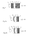
- a microchip laser according to a fifth embodiment of the invention is shown in Fig. 7.
- the laser in Fig. 7 differs from the one in Fig. 1 in that a mechanically supporting element 13 is provided on opposite sides of the laser microchip 1.
- This realization is particularly preferred in high power applications.
- the mechanically supporting elements 13 counteracts such an undesired cracking by reducing the thermal expansion of the laser microchip 1 .
- the mechanically supporting elements 13 is preferably made of the same material as the laser microchip 1, but without doping. If the laser microchip is made of Nd:YAG, it is consequently preferred to have the mechanically supporting elements 13 made of undoped YAG.
- a microchip laser according to a seventh embodiment of the invention is shown.
- the laser in Fig. 8a is different from, for example, the one shown in Fig. 1 in that it has the side 1a opposite to the quasi-phase matching element 2 polished to a curved surface on which a curved reflecting element 3a is provided.
- the curved reflecting element 3a works as a converging element which both forms a stable laser cavity and achieves the highest possible light intensity in the quasi-phase matching element 2, which schematically is indicated with dashed lines in the figure. It may be noted that a completely planar parallel microchip laser of the kind shown in Fig.
- the converging element is provided in a similar way by a reflecting element 3a, which corresponds to the curved reflecting element 3a in Fig. 8a but which in Fig. 8b instead is provided on a curved surface of a mirror substrate 14a.
- a reflecting element 3a which corresponds to the curved reflecting element 3a in Fig. 8a but which in Fig. 8b instead is provided on a curved surface of a mirror substrate 14a.
- One side of the substrate 14a is essentially planar, while the other side of the substrate 14a, i.e. the side directed towards the laser microchip 1 and covered with the reflecting element 3a, is curved and hence only in contact with the laser micro-chip 1 in a peripheral portion thereof.
- the reflecting element 3a may be completely separated from the laser microchip 1.
- the reflecting element 3a is preferentially high reflecting for the fundamental wavelength. It is at the same time preferred that the element 3a transmits light from the laser diode 7 so it easily can pass into the laser cavity. As a consequence of the curvature of the substrate 14a and the reflecting element 3a, a semi-convex air gap is formed between the reflecting element 3a and the laser chip 1.
- the curved surface of the reflecting element 3a will provide a stabilization of the beam path through the laser and a focusing of the light in the quasi-phase matching element, in a similar way as is described with reference to Fig. 8a and which has been indicated by the dashed lines in Fig. 8b.
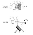
- Fig. 9a and 9b schematically show a miniature laser according to an eighth embodiment of the invention.
- a first reflecting element 3, a laser microchip 1, a quasi-phase matching element 2, and a second reflecting element 4 are arranged separately from each other on a prepared micro-table or carrier 10, which may be a silicon chip, a plastic plate, an etched glass or metal plate, or the like.
- the laser microchip is pumped by a laser diode 7 via an optical fiber 8.
- the laser light may instead be transferred from the diode laser 7 directly to the laser micro-chip 1 without any optical fiber, or by using a lens system or the like.
- the elements are mounted separately from each other on the carriers 10. This facilities fine adjustments of the different elements to allow optimization of the function of the miniature laser.
- the reflecting elements 3 and 4 may be chosen, and their individual positions be adjusted, to give an optimized beam path through the cavity formed by the reflecting elements 3 and 4. It is desired that the beam path is adjusted so that an optimum power density is achieved in the quasi-phase matching element 2.
- the carrier 10 be provided with tuning nobs, or similar tools (not shown), to trim the position of the different elements.
- a quasi-phase matching element which only has one grating period can be rotated or tilted around the axes perpendicular to the beam path through the cavity, as shown in Fig. 9b.
- the grating period can hence be mechanically adjusted for optimum frequency doubling.
- the miniature laser in Fig. 9a and 9b may of course also include other elements, like a tunable mode discriminating element for choice of desired laser mode.
- a miniature laser of the kind shown in Fig. 9a and 9b may also be provided with light converging elements aiming to stabilize the laser and provide an optimum light intensity in the quasi-phase matching element 2.
- a converging element in the form of a conventional convex lens 14b, is provided between the laser chip 1 and the quasi-phase matching element 2.
- the lens 14b in Fig. 9c is separated from the laser chip 1 and the element 2 by air gaps.
- the lens 14a will stabilize the beam path through the laser and at the same time focus the beam in the quasi-phase matching element, in a similar way as described with reference to Fig. 8a and 8b.
- a converging element is provided in form of a curved mirror 15 arranged between the laser chip 12 and the quasi-phase matching element 2.
- a folded beam path through the cavity is utilized, defined by the reflecting elements 3, 4 and 15.
- the mirror 15 will reflect and focus the light from the laser microchip 1 on the quasi-phase matching element 2 to provide both a stabilization of the beam path through the laser and a focusing of the light to a high intensity in the quasi-phase matching element, in a similar way to what has been described above.
Landscapes
- Physics & Mathematics (AREA)
- Electromagnetism (AREA)
- Engineering & Computer Science (AREA)
- Plasma & Fusion (AREA)
- Optics & Photonics (AREA)
- Nonlinear Science (AREA)
- Lasers (AREA)
- Optical Modulation, Optical Deflection, Nonlinear Optics, Optical Demodulation, Optical Logic Elements (AREA)
Applications Claiming Priority (3)
| Application Number | Priority Date | Filing Date | Title |
|---|---|---|---|
| SE9603234 | 1996-09-05 | ||
| SE9603234A SE510442C2 (sv) | 1996-09-05 | 1996-09-05 | Mikrochipslaser |
| PCT/SE1997/001466 WO1998010497A1 (en) | 1996-09-05 | 1997-09-02 | Laser |
Publications (2)
| Publication Number | Publication Date |
|---|---|
| EP0923799A1 EP0923799A1 (en) | 1999-06-23 |
| EP0923799B1 true EP0923799B1 (en) | 2004-11-03 |
Family
ID=20403783
Family Applications (1)
| Application Number | Title | Priority Date | Filing Date |
|---|---|---|---|
| EP97939284A Expired - Lifetime EP0923799B1 (en) | 1996-09-05 | 1997-09-02 | Frequency doubled laser with an intracavity nonlinear, quasi-phase matching element |
Country Status (8)
| Country | Link |
|---|---|
| US (1) | US6259711B1 (sv) |
| EP (1) | EP0923799B1 (sv) |
| JP (1) | JP2000517481A (sv) |
| AT (1) | ATE281704T1 (sv) |
| CA (1) | CA2264753A1 (sv) |
| DE (1) | DE69731475T2 (sv) |
| SE (1) | SE510442C2 (sv) |
| WO (1) | WO1998010497A1 (sv) |
Families Citing this family (32)
| Publication number | Priority date | Publication date | Assignee | Title |
|---|---|---|---|---|
| US7046711B2 (en) * | 1999-06-11 | 2006-05-16 | High Q Laser Production Gmbh | High power and high gain saturation diode pumped laser means and diode array pumping device |
| FR2795248B1 (fr) * | 1999-06-21 | 2004-11-12 | Lprl Laboratoire De Physique D | Source monochromatique comprenant un materiau optiquement actif |
| DE19939774C2 (de) * | 1999-08-21 | 2001-06-28 | Rofin Sinar Laser Gmbh | Festkörperlaser (Scheibenlaser) mit direktem Kontakt des aktiven Mediums zu einer Kühlmittelflüssigkeit |
| US6373865B1 (en) * | 2000-02-01 | 2002-04-16 | John E. Nettleton | Pseudo-monolithic laser with an intracavity optical parametric oscillator |
| US6633596B1 (en) * | 2000-05-31 | 2003-10-14 | University Corporation For Atmospheric Research | Frequency stable pulsed laser |
| US6914921B2 (en) * | 2001-09-28 | 2005-07-05 | The Furukawa Electric Company, Ltd. | Optical filter, laser module, and wavelength locker module |
| DE10204796A1 (de) * | 2002-02-01 | 2003-08-21 | Ozygus Bernd | Lasergainmodul |
| US20040076204A1 (en) * | 2002-10-16 | 2004-04-22 | Kruschwitz Brian E. | External cavity organic laser |
| JP2004296706A (ja) * | 2003-03-26 | 2004-10-21 | Sony Corp | 光共振器及びレーザ発振器 |
| TW574031B (en) * | 2003-04-11 | 2004-02-01 | Applied Biophotonics Corp | Quasi-phase-matching photodynamic therapy (PDT) and photodynamic diagnosis (PDD) laser sources |
| JP2006310743A (ja) * | 2005-03-31 | 2006-11-09 | Topcon Corp | レーザ発振装置 |
| FR2884651B1 (fr) * | 2005-04-15 | 2007-11-30 | Oxxius Sa Sa | "dispositif laser lineaire monolithique monofrequence, et systeme comprenant un tel dispositif" |
| EP1722449B1 (de) * | 2005-05-12 | 2008-10-22 | Innovavent GmbH | Verwendung eines Scheibenlasers zur Kristallisation von Siliziumschichten |
| EP1888914B1 (de) * | 2005-05-27 | 2012-07-11 | Robert Bosch Gmbh | Zündeinrichtung für eine brennkraftmaschine |
| JP2007158020A (ja) * | 2005-12-05 | 2007-06-21 | Ricoh Co Ltd | 光学素子 |
| KR20070076251A (ko) * | 2006-01-18 | 2007-07-24 | 삼성전자주식회사 | 외부 공진기형 면발광 레이저 |
| CN101395772B (zh) * | 2006-03-03 | 2011-01-26 | 松下电器产业株式会社 | 照明光源及激光投影装置 |
| US7570676B2 (en) * | 2006-05-09 | 2009-08-04 | Spectralus Corporation | Compact efficient and robust ultraviolet solid-state laser sources based on nonlinear frequency conversion in periodically poled materials |
| KR100764424B1 (ko) * | 2006-08-30 | 2007-10-05 | 삼성전기주식회사 | 파장변환 레이저 장치 및 이에 사용되는 비선형 광학결정 |
| JP2008177226A (ja) * | 2007-01-16 | 2008-07-31 | Cyber Laser Kk | レーザパルス発生装置及び方法 |
| US7573930B2 (en) * | 2007-06-14 | 2009-08-11 | Innovavent Gmbh | Anamorphotic solid-sate laser |
| JP2009259914A (ja) * | 2008-04-14 | 2009-11-05 | Sony Corp | レーザ装置、レーザディスプレイ装置およびレーザ照射装置 |
| JP2010109070A (ja) * | 2008-10-29 | 2010-05-13 | Osaka Prefecture Univ | 多波長レーザー発振装置およびそれを備えてなるテラヘルツ波発生装置 |
| EP2680377B1 (en) | 2012-06-29 | 2017-05-10 | C2C Link Corporation | Method for making a laser module |
| US9197027B2 (en) | 2012-07-05 | 2015-11-24 | C2C Link Corporation | Method for making laser module |
| CN103050870B (zh) * | 2012-10-17 | 2015-07-15 | 北京工业大学 | 可光纤输出的微片激光器 |
| JP6281935B2 (ja) * | 2013-10-25 | 2018-02-21 | 大学共同利用機関法人自然科学研究機構 | Qスイッチレーザー装置 |
| FR3025661B1 (fr) * | 2014-09-05 | 2016-11-25 | Oxxius | Systeme de generation de faisceau laser par effet non lineaire a base de cavite microchip resonante |
| CN111095694A (zh) | 2017-09-05 | 2020-05-01 | 国立研究开发法人量子科学技术研究开发机构 | 激光装置、光源以及测量装置 |
| JP6771442B2 (ja) * | 2017-09-20 | 2020-10-21 | 株式会社東芝 | 光学素子 |
| FR3078571B1 (fr) * | 2018-03-01 | 2020-02-07 | Blue Industry And Science | Oscillateur parametrique optique |
| JP7343914B2 (ja) * | 2021-01-14 | 2023-09-13 | 大学共同利用機関法人自然科学研究機構 | レーザ発振器 |
Family Cites Families (26)
| Publication number | Priority date | Publication date | Assignee | Title |
|---|---|---|---|---|
| US4723257A (en) | 1986-05-19 | 1988-02-02 | Spectra-Physics, Inc. | Laser diode pumped solid state laser with miniaturized laser head |
| US4953166A (en) * | 1988-02-02 | 1990-08-28 | Massachusetts Institute Of Technology | Microchip laser |
| US4860304A (en) | 1988-02-02 | 1989-08-22 | Massachusetts Institute Of Technology | Solid state microlaser |
| US5256164A (en) * | 1988-02-02 | 1993-10-26 | Massachusetts Institute Of Technology | Method of fabricating a microchip laser |
| US5265116A (en) * | 1988-02-02 | 1993-11-23 | Massachusetts Institute Of Technology | Microchip laser |
| US4847851A (en) | 1988-05-19 | 1989-07-11 | University Of South Florida | Butt-coupled single transverse mode diode pumped laser |
| US4982405A (en) | 1989-09-07 | 1991-01-01 | Massachusette Institute Of Technology | Coupled-cavity Q-switched laser |
| US5132977A (en) | 1989-09-07 | 1992-07-21 | Massachusetts Institute Of Technology | Coupled-cavity Q-switched laser |
| US5341393A (en) | 1990-05-10 | 1994-08-23 | Fuji Photo Film Co., Ltd. | Laser-diode-pumped solid-state laser |
| US5187714A (en) | 1990-10-19 | 1993-02-16 | Fuji Photo Film Co., Ltd. | Laser-diode-pumped solid-state laser |
| US5119382A (en) | 1990-12-24 | 1992-06-02 | Mcdonnell Douglas Corporation | Tetravalent chromium doped passive Q-switch |
| US5315433A (en) | 1991-02-28 | 1994-05-24 | Fuji Photo Film Co., Ltd. | Optical wavelength converting apparatus |
| JP2654726B2 (ja) | 1991-09-11 | 1997-09-17 | 富士写真フイルム株式会社 | レーザーダイオードポンピング固体レーザー |
| US5278855A (en) | 1992-05-11 | 1994-01-11 | At&T Bell Laboratories | Broadband semiconductor saturable absorber |
| US5289491A (en) * | 1993-03-22 | 1994-02-22 | Amoco Corporation | Intracavity harmonic sub-resonator with extended phase matching range |
| EP0715774B1 (en) | 1993-08-26 | 2000-05-17 | Laser Power Corporation | Deep blue microlaser |
| US5425039A (en) * | 1994-02-24 | 1995-06-13 | Micron Optics, Inc. | Single-frequency fiber Fabry-Perot micro lasers |
| US5388114A (en) * | 1994-03-17 | 1995-02-07 | Polaroid Corporation | Miniaturized self-Q-switched frequency-doubled laser |
| US5511085A (en) * | 1994-09-02 | 1996-04-23 | Light Solutions Corporation | Passively stabilized intracavity doubling laser |
| SE504584C2 (sv) | 1994-12-07 | 1997-03-10 | Fredrik Laurell | Anordning för alstring av frekvensdubblerat laserljus medelst kvasifasmatchning |
| FR2734094B1 (fr) * | 1995-05-12 | 1997-06-06 | Commissariat Energie Atomique | Emetteur infrarouge monolithique a semi-conducteur pompe par un microlaser solide declenche |
| FR2734092B1 (fr) * | 1995-05-12 | 1997-06-06 | Commissariat Energie Atomique | Microlaser monolithique declenche et materiau non lineaire intracavite |
| FR2734093B1 (fr) * | 1995-05-12 | 1997-06-06 | Commissariat Energie Atomique | Oscillateur parametrique optique monolithique pompe par un microlaser |
| GB2300964B (en) | 1995-05-13 | 1999-11-10 | I E Optomech Limited | Monolithic laser |
| US5585962A (en) | 1995-06-07 | 1996-12-17 | Amoco Corporation | External resonant frequency mixers based on degenerate and half-degenerate resonators |
| US5982789A (en) * | 1995-11-22 | 1999-11-09 | Light Solutions Corporation | Pulsed laser with passive stabilization |
-
1996
- 1996-09-05 SE SE9603234A patent/SE510442C2/sv unknown
-
1997
- 1997-09-02 AT AT97939284T patent/ATE281704T1/de not_active IP Right Cessation
- 1997-09-02 JP JP10512566A patent/JP2000517481A/ja active Pending
- 1997-09-02 EP EP97939284A patent/EP0923799B1/en not_active Expired - Lifetime
- 1997-09-02 DE DE69731475T patent/DE69731475T2/de not_active Expired - Lifetime
- 1997-09-02 US US09/242,892 patent/US6259711B1/en not_active Expired - Lifetime
- 1997-09-02 CA CA002264753A patent/CA2264753A1/en not_active Abandoned
- 1997-09-02 WO PCT/SE1997/001466 patent/WO1998010497A1/en active IP Right Grant
Non-Patent Citations (1)
| Title |
|---|
| TAIRA T. AND KOBAYASHI T.: "Intracavity frequency doubling and Q-switching in diode-laser-pumped Nd:YVO4 lasers", APPLIED OPTICS, vol. 34, no. 21, 20 August 1995 (1995-08-20), pages 4298 - 4301, XP000517287, DOI: doi:10.1364/AO.34.004298 * |
Also Published As
| Publication number | Publication date |
|---|---|
| EP0923799A1 (en) | 1999-06-23 |
| SE510442C2 (sv) | 1999-05-25 |
| SE9603234D0 (sv) | 1996-09-05 |
| CA2264753A1 (en) | 1998-03-12 |
| ATE281704T1 (de) | 2004-11-15 |
| US6259711B1 (en) | 2001-07-10 |
| SE9603234L (sv) | 1998-03-06 |
| DE69731475T2 (de) | 2005-10-20 |
| DE69731475D1 (de) | 2004-12-09 |
| WO1998010497A1 (en) | 1998-03-12 |
| JP2000517481A (ja) | 2000-12-26 |
Similar Documents
| Publication | Publication Date | Title |
|---|---|---|
| EP0923799B1 (en) | Frequency doubled laser with an intracavity nonlinear, quasi-phase matching element | |
| US4739507A (en) | Diode end pumped laser and harmonic generator using same | |
| Zayhowski | Microchip lasers | |
| US5854802A (en) | Single longitudinal mode frequency converted laser | |
| US5218610A (en) | Tunable solid state laser | |
| US5499256A (en) | Polarized frequency-selective optical source | |
| EP0742966B1 (en) | Diode pumped, multi axial mode, intracavity frequency doubled laser | |
| US5063566A (en) | Internally-doubled, composite-cavity microlaser | |
| CA2185692C (en) | Miniaturized self-q-switched frequency-doubled laser | |
| EP0452069B1 (en) | Ring laser | |
| US4942582A (en) | Single frequency solid state laser | |
| US5197072A (en) | Optical wavelength converting device, and laser diode pumped solid laser | |
| US5172391A (en) | Polarization controlling system for lasers | |
| EP1180836A2 (en) | Microlaser assembly having a microresonator and aligned electro-optic components | |
| JP3683360B2 (ja) | 偏光制御素子および固体レーザー | |
| JP3614474B2 (ja) | 波長変換レーザー | |
| US6628692B2 (en) | Solid-state laser device and solid-state laser amplifier provided therewith | |
| US6047014A (en) | Solid state laser and method of manufacturing the same | |
| CN106229803B (zh) | 一种光纤基单频蓝光脉冲激光器 | |
| US8649404B2 (en) | Compact and efficient visible laser source with high speed modulation | |
| JPH04229690A (ja) | 弱吸収レーザ材をポンピングするための装置及び方法 | |
| JP2761678B2 (ja) | レーザーダイオードポンピング固体レーザー | |
| KR100366699B1 (ko) | 내부 공진형 제2 고조파 발생 장치 | |
| KR101156637B1 (ko) | 주기적 분극 재료를 이용하여 비선형 주파수 변환을 하는소형 고체상태 레이저 | |
| JP2663197B2 (ja) | レーザーダイオードポンピング固体レーザー |
Legal Events
| Date | Code | Title | Description |
|---|---|---|---|
| PUAI | Public reference made under article 153(3) epc to a published international application that has entered the european phase |
Free format text: ORIGINAL CODE: 0009012 |
|
| 17P | Request for examination filed |
Effective date: 19990301 |
|
| AK | Designated contracting states |
Kind code of ref document: A1 Designated state(s): AT BE CH DE DK ES FI FR GB IE IT LI NL SE |
|
| RAP1 | Party data changed (applicant data changed or rights of an application transferred) |
Owner name: COBOLT AB |
|
| RIN1 | Information on inventor provided before grant (corrected) |
Inventor name: LAURELL, FREDRIK |
|
| 17Q | First examination report despatched |
Effective date: 20021104 |
|
| RTI1 | Title (correction) |
Free format text: FREQUENCY DOUBLED LASER WITH AN INTRACAVITY NONLINEAR, QUASI-PHASE MATCHING ELEMENT |
|
| GRAP | Despatch of communication of intention to grant a patent |
Free format text: ORIGINAL CODE: EPIDOSNIGR1 |
|
| RTI1 | Title (correction) |
Free format text: FREQUENCY DOUBLED LASER WITH AN INTRACAVITY NONLINEAR, QUASI-PHASE MATCHING ELEMENT |
|
| GRAS | Grant fee paid |
Free format text: ORIGINAL CODE: EPIDOSNIGR3 |
|
| GRAA | (expected) grant |
Free format text: ORIGINAL CODE: 0009210 |
|
| AK | Designated contracting states |
Kind code of ref document: B1 Designated state(s): AT BE CH DE DK ES FI FR GB IE IT LI NL SE |
|
| PG25 | Lapsed in a contracting state [announced via postgrant information from national office to epo] |
Ref country code: NL Free format text: LAPSE BECAUSE OF FAILURE TO SUBMIT A TRANSLATION OF THE DESCRIPTION OR TO PAY THE FEE WITHIN THE PRESCRIBED TIME-LIMIT Effective date: 20041103 Ref country code: LI Free format text: LAPSE BECAUSE OF FAILURE TO SUBMIT A TRANSLATION OF THE DESCRIPTION OR TO PAY THE FEE WITHIN THE PRESCRIBED TIME-LIMIT Effective date: 20041103 Ref country code: IT Free format text: LAPSE BECAUSE OF FAILURE TO SUBMIT A TRANSLATION OF THE DESCRIPTION OR TO PAY THE FEE WITHIN THE PRESCRIBED TIME-LIMIT;WARNING: LAPSES OF ITALIAN PATENTS WITH EFFECTIVE DATE BEFORE 2007 MAY HAVE OCCURRED AT ANY TIME BEFORE 2007. THE CORRECT EFFECTIVE DATE MAY BE DIFFERENT FROM THE ONE RECORDED. Effective date: 20041103 Ref country code: FI Free format text: LAPSE BECAUSE OF FAILURE TO SUBMIT A TRANSLATION OF THE DESCRIPTION OR TO PAY THE FEE WITHIN THE PRESCRIBED TIME-LIMIT Effective date: 20041103 Ref country code: CH Free format text: LAPSE BECAUSE OF FAILURE TO SUBMIT A TRANSLATION OF THE DESCRIPTION OR TO PAY THE FEE WITHIN THE PRESCRIBED TIME-LIMIT Effective date: 20041103 Ref country code: BE Free format text: LAPSE BECAUSE OF FAILURE TO SUBMIT A TRANSLATION OF THE DESCRIPTION OR TO PAY THE FEE WITHIN THE PRESCRIBED TIME-LIMIT Effective date: 20041103 Ref country code: AT Free format text: LAPSE BECAUSE OF FAILURE TO SUBMIT A TRANSLATION OF THE DESCRIPTION OR TO PAY THE FEE WITHIN THE PRESCRIBED TIME-LIMIT Effective date: 20041103 |
|
| REG | Reference to a national code |
Ref country code: GB Ref legal event code: FG4D |
|
| REG | Reference to a national code |
Ref country code: CH Ref legal event code: EP |
|
| REF | Corresponds to: |
Ref document number: 69731475 Country of ref document: DE Date of ref document: 20041209 Kind code of ref document: P |
|
| REG | Reference to a national code |
Ref country code: IE Ref legal event code: FG4D |
|
| RAP2 | Party data changed (patent owner data changed or rights of a patent transferred) |
Owner name: COBOLT AB |
|
| PG25 | Lapsed in a contracting state [announced via postgrant information from national office to epo] |
Ref country code: SE Free format text: LAPSE BECAUSE OF FAILURE TO SUBMIT A TRANSLATION OF THE DESCRIPTION OR TO PAY THE FEE WITHIN THE PRESCRIBED TIME-LIMIT Effective date: 20050203 Ref country code: DK Free format text: LAPSE BECAUSE OF FAILURE TO SUBMIT A TRANSLATION OF THE DESCRIPTION OR TO PAY THE FEE WITHIN THE PRESCRIBED TIME-LIMIT Effective date: 20050203 |
|
| PG25 | Lapsed in a contracting state [announced via postgrant information from national office to epo] |
Ref country code: ES Free format text: LAPSE BECAUSE OF FAILURE TO SUBMIT A TRANSLATION OF THE DESCRIPTION OR TO PAY THE FEE WITHIN THE PRESCRIBED TIME-LIMIT Effective date: 20050214 |
|
| NLT2 | Nl: modifications (of names), taken from the european patent patent bulletin |
Owner name: COBOLT AB |
|
| NLV1 | Nl: lapsed or annulled due to failure to fulfill the requirements of art. 29p and 29m of the patents act | ||
| REG | Reference to a national code |
Ref country code: CH Ref legal event code: PL |
|
| PG25 | Lapsed in a contracting state [announced via postgrant information from national office to epo] |
Ref country code: IE Free format text: LAPSE BECAUSE OF NON-PAYMENT OF DUE FEES Effective date: 20050902 |
|
| PLBE | No opposition filed within time limit |
Free format text: ORIGINAL CODE: 0009261 |
|
| STAA | Information on the status of an ep patent application or granted ep patent |
Free format text: STATUS: NO OPPOSITION FILED WITHIN TIME LIMIT |
|
| 26N | No opposition filed |
Effective date: 20050804 |
|
| ET | Fr: translation filed | ||
| REG | Reference to a national code |
Ref country code: IE Ref legal event code: MM4A |
|
| REG | Reference to a national code |
Ref country code: FR Ref legal event code: PLFP Year of fee payment: 19 |
|
| PGFP | Annual fee paid to national office [announced via postgrant information from national office to epo] |
Ref country code: DE Payment date: 20150903 Year of fee payment: 19 Ref country code: GB Payment date: 20150904 Year of fee payment: 19 |
|
| PGFP | Annual fee paid to national office [announced via postgrant information from national office to epo] |
Ref country code: FR Payment date: 20150916 Year of fee payment: 19 |
|
| REG | Reference to a national code |
Ref country code: DE Ref legal event code: R119 Ref document number: 69731475 Country of ref document: DE |
|
| GBPC | Gb: european patent ceased through non-payment of renewal fee |
Effective date: 20160902 |
|
| REG | Reference to a national code |
Ref country code: FR Ref legal event code: ST Effective date: 20170531 |
|
| PG25 | Lapsed in a contracting state [announced via postgrant information from national office to epo] |
Ref country code: FR Free format text: LAPSE BECAUSE OF NON-PAYMENT OF DUE FEES Effective date: 20160930 Ref country code: GB Free format text: LAPSE BECAUSE OF NON-PAYMENT OF DUE FEES Effective date: 20160902 Ref country code: DE Free format text: LAPSE BECAUSE OF NON-PAYMENT OF DUE FEES Effective date: 20170401 |