EP0922780B1 - Method of manufacturing a high purity hard gold alloy - Google Patents
Method of manufacturing a high purity hard gold alloy Download PDFInfo
- Publication number
- EP0922780B1 EP0922780B1 EP97927367A EP97927367A EP0922780B1 EP 0922780 B1 EP0922780 B1 EP 0922780B1 EP 97927367 A EP97927367 A EP 97927367A EP 97927367 A EP97927367 A EP 97927367A EP 0922780 B1 EP0922780 B1 EP 0922780B1
- Authority
- EP
- European Patent Office
- Prior art keywords
- alloy
- gold
- high purity
- gold alloy
- members
- Prior art date
- Legal status (The legal status is an assumption and is not a legal conclusion. Google has not performed a legal analysis and makes no representation as to the accuracy of the status listed.)
- Expired - Lifetime
Links
Images


Classifications
-
- C—CHEMISTRY; METALLURGY
- C22—METALLURGY; FERROUS OR NON-FERROUS ALLOYS; TREATMENT OF ALLOYS OR NON-FERROUS METALS
- C22F—CHANGING THE PHYSICAL STRUCTURE OF NON-FERROUS METALS AND NON-FERROUS ALLOYS
- C22F1/00—Changing the physical structure of non-ferrous metals or alloys by heat treatment or by hot or cold working
- C22F1/14—Changing the physical structure of non-ferrous metals or alloys by heat treatment or by hot or cold working of noble metals or alloys based thereon
-
- C—CHEMISTRY; METALLURGY
- C22—METALLURGY; FERROUS OR NON-FERROUS ALLOYS; TREATMENT OF ALLOYS OR NON-FERROUS METALS
- C22C—ALLOYS
- C22C5/00—Alloys based on noble metals
- C22C5/02—Alloys based on gold
-
- H—ELECTRICITY
- H01—ELECTRIC ELEMENTS
- H01L—SEMICONDUCTOR DEVICES NOT COVERED BY CLASS H10
- H01L24/00—Arrangements for connecting or disconnecting semiconductor or solid-state bodies; Methods or apparatus related thereto
- H01L24/01—Means for bonding being attached to, or being formed on, the surface to be connected, e.g. chip-to-package, die-attach, "first-level" interconnects; Manufacturing methods related thereto
- H01L24/42—Wire connectors; Manufacturing methods related thereto
- H01L24/43—Manufacturing methods
-
- H—ELECTRICITY
- H01—ELECTRIC ELEMENTS
- H01L—SEMICONDUCTOR DEVICES NOT COVERED BY CLASS H10
- H01L24/00—Arrangements for connecting or disconnecting semiconductor or solid-state bodies; Methods or apparatus related thereto
- H01L24/01—Means for bonding being attached to, or being formed on, the surface to be connected, e.g. chip-to-package, die-attach, "first-level" interconnects; Manufacturing methods related thereto
- H01L24/42—Wire connectors; Manufacturing methods related thereto
- H01L24/44—Structure, shape, material or disposition of the wire connectors prior to the connecting process
- H01L24/45—Structure, shape, material or disposition of the wire connectors prior to the connecting process of an individual wire connector
-
- H—ELECTRICITY
- H01—ELECTRIC ELEMENTS
- H01L—SEMICONDUCTOR DEVICES NOT COVERED BY CLASS H10
- H01L2224/00—Indexing scheme for arrangements for connecting or disconnecting semiconductor or solid-state bodies and methods related thereto as covered by H01L24/00
- H01L2224/01—Means for bonding being attached to, or being formed on, the surface to be connected, e.g. chip-to-package, die-attach, "first-level" interconnects; Manufacturing methods related thereto
- H01L2224/42—Wire connectors; Manufacturing methods related thereto
- H01L2224/43—Manufacturing methods
-
- H—ELECTRICITY
- H01—ELECTRIC ELEMENTS
- H01L—SEMICONDUCTOR DEVICES NOT COVERED BY CLASS H10
- H01L2224/00—Indexing scheme for arrangements for connecting or disconnecting semiconductor or solid-state bodies and methods related thereto as covered by H01L24/00
- H01L2224/01—Means for bonding being attached to, or being formed on, the surface to be connected, e.g. chip-to-package, die-attach, "first-level" interconnects; Manufacturing methods related thereto
- H01L2224/42—Wire connectors; Manufacturing methods related thereto
- H01L2224/44—Structure, shape, material or disposition of the wire connectors prior to the connecting process
- H01L2224/45—Structure, shape, material or disposition of the wire connectors prior to the connecting process of an individual wire connector
- H01L2224/45001—Core members of the connector
- H01L2224/4501—Shape
- H01L2224/45012—Cross-sectional shape
- H01L2224/45015—Cross-sectional shape being circular
-
- H—ELECTRICITY
- H01—ELECTRIC ELEMENTS
- H01L—SEMICONDUCTOR DEVICES NOT COVERED BY CLASS H10
- H01L2224/00—Indexing scheme for arrangements for connecting or disconnecting semiconductor or solid-state bodies and methods related thereto as covered by H01L24/00
- H01L2224/01—Means for bonding being attached to, or being formed on, the surface to be connected, e.g. chip-to-package, die-attach, "first-level" interconnects; Manufacturing methods related thereto
- H01L2224/42—Wire connectors; Manufacturing methods related thereto
- H01L2224/44—Structure, shape, material or disposition of the wire connectors prior to the connecting process
- H01L2224/45—Structure, shape, material or disposition of the wire connectors prior to the connecting process of an individual wire connector
- H01L2224/45001—Core members of the connector
- H01L2224/45099—Material
- H01L2224/451—Material with a principal constituent of the material being a metal or a metalloid, e.g. boron (B), silicon (Si), germanium (Ge), arsenic (As), antimony (Sb), tellurium (Te) and polonium (Po), and alloys thereof
- H01L2224/45138—Material with a principal constituent of the material being a metal or a metalloid, e.g. boron (B), silicon (Si), germanium (Ge), arsenic (As), antimony (Sb), tellurium (Te) and polonium (Po), and alloys thereof the principal constituent melting at a temperature of greater than or equal to 950°C and less than 1550°C
- H01L2224/45144—Gold (Au) as principal constituent
-
- H—ELECTRICITY
- H01—ELECTRIC ELEMENTS
- H01L—SEMICONDUCTOR DEVICES NOT COVERED BY CLASS H10
- H01L2924/00—Indexing scheme for arrangements or methods for connecting or disconnecting semiconductor or solid-state bodies as covered by H01L24/00
- H01L2924/0001—Technical content checked by a classifier
- H01L2924/00011—Not relevant to the scope of the group, the symbol of which is combined with the symbol of this group
-
- H—ELECTRICITY
- H01—ELECTRIC ELEMENTS
- H01L—SEMICONDUCTOR DEVICES NOT COVERED BY CLASS H10
- H01L2924/00—Indexing scheme for arrangements or methods for connecting or disconnecting semiconductor or solid-state bodies as covered by H01L24/00
- H01L2924/0001—Technical content checked by a classifier
- H01L2924/00014—Technical content checked by a classifier the subject-matter covered by the group, the symbol of which is combined with the symbol of this group, being disclosed without further technical details
-
- H—ELECTRICITY
- H01—ELECTRIC ELEMENTS
- H01L—SEMICONDUCTOR DEVICES NOT COVERED BY CLASS H10
- H01L2924/00—Indexing scheme for arrangements or methods for connecting or disconnecting semiconductor or solid-state bodies as covered by H01L24/00
- H01L2924/01—Chemical elements
- H01L2924/01005—Boron [B]
-
- H—ELECTRICITY
- H01—ELECTRIC ELEMENTS
- H01L—SEMICONDUCTOR DEVICES NOT COVERED BY CLASS H10
- H01L2924/00—Indexing scheme for arrangements or methods for connecting or disconnecting semiconductor or solid-state bodies as covered by H01L24/00
- H01L2924/01—Chemical elements
- H01L2924/01006—Carbon [C]
-
- H—ELECTRICITY
- H01—ELECTRIC ELEMENTS
- H01L—SEMICONDUCTOR DEVICES NOT COVERED BY CLASS H10
- H01L2924/00—Indexing scheme for arrangements or methods for connecting or disconnecting semiconductor or solid-state bodies as covered by H01L24/00
- H01L2924/01—Chemical elements
- H01L2924/01013—Aluminum [Al]
-
- H—ELECTRICITY
- H01—ELECTRIC ELEMENTS
- H01L—SEMICONDUCTOR DEVICES NOT COVERED BY CLASS H10
- H01L2924/00—Indexing scheme for arrangements or methods for connecting or disconnecting semiconductor or solid-state bodies as covered by H01L24/00
- H01L2924/01—Chemical elements
- H01L2924/01014—Silicon [Si]
-
- H—ELECTRICITY
- H01—ELECTRIC ELEMENTS
- H01L—SEMICONDUCTOR DEVICES NOT COVERED BY CLASS H10
- H01L2924/00—Indexing scheme for arrangements or methods for connecting or disconnecting semiconductor or solid-state bodies as covered by H01L24/00
- H01L2924/01—Chemical elements
- H01L2924/01029—Copper [Cu]
-
- H—ELECTRICITY
- H01—ELECTRIC ELEMENTS
- H01L—SEMICONDUCTOR DEVICES NOT COVERED BY CLASS H10
- H01L2924/00—Indexing scheme for arrangements or methods for connecting or disconnecting semiconductor or solid-state bodies as covered by H01L24/00
- H01L2924/01—Chemical elements
- H01L2924/01039—Yttrium [Y]
-
- H—ELECTRICITY
- H01—ELECTRIC ELEMENTS
- H01L—SEMICONDUCTOR DEVICES NOT COVERED BY CLASS H10
- H01L2924/00—Indexing scheme for arrangements or methods for connecting or disconnecting semiconductor or solid-state bodies as covered by H01L24/00
- H01L2924/01—Chemical elements
- H01L2924/01049—Indium [In]
-
- H—ELECTRICITY
- H01—ELECTRIC ELEMENTS
- H01L—SEMICONDUCTOR DEVICES NOT COVERED BY CLASS H10
- H01L2924/00—Indexing scheme for arrangements or methods for connecting or disconnecting semiconductor or solid-state bodies as covered by H01L24/00
- H01L2924/01—Chemical elements
- H01L2924/01051—Antimony [Sb]
-
- H—ELECTRICITY
- H01—ELECTRIC ELEMENTS
- H01L—SEMICONDUCTOR DEVICES NOT COVERED BY CLASS H10
- H01L2924/00—Indexing scheme for arrangements or methods for connecting or disconnecting semiconductor or solid-state bodies as covered by H01L24/00
- H01L2924/01—Chemical elements
- H01L2924/01057—Lanthanum [La]
-
- H—ELECTRICITY
- H01—ELECTRIC ELEMENTS
- H01L—SEMICONDUCTOR DEVICES NOT COVERED BY CLASS H10
- H01L2924/00—Indexing scheme for arrangements or methods for connecting or disconnecting semiconductor or solid-state bodies as covered by H01L24/00
- H01L2924/01—Chemical elements
- H01L2924/01058—Cerium [Ce]
-
- H—ELECTRICITY
- H01—ELECTRIC ELEMENTS
- H01L—SEMICONDUCTOR DEVICES NOT COVERED BY CLASS H10
- H01L2924/00—Indexing scheme for arrangements or methods for connecting or disconnecting semiconductor or solid-state bodies as covered by H01L24/00
- H01L2924/01—Chemical elements
- H01L2924/01064—Gadolinium [Gd]
-
- H—ELECTRICITY
- H01—ELECTRIC ELEMENTS
- H01L—SEMICONDUCTOR DEVICES NOT COVERED BY CLASS H10
- H01L2924/00—Indexing scheme for arrangements or methods for connecting or disconnecting semiconductor or solid-state bodies as covered by H01L24/00
- H01L2924/01—Chemical elements
- H01L2924/0107—Ytterbium [Yb]
-
- H—ELECTRICITY
- H01—ELECTRIC ELEMENTS
- H01L—SEMICONDUCTOR DEVICES NOT COVERED BY CLASS H10
- H01L2924/00—Indexing scheme for arrangements or methods for connecting or disconnecting semiconductor or solid-state bodies as covered by H01L24/00
- H01L2924/01—Chemical elements
- H01L2924/01075—Rhenium [Re]
-
- H—ELECTRICITY
- H01—ELECTRIC ELEMENTS
- H01L—SEMICONDUCTOR DEVICES NOT COVERED BY CLASS H10
- H01L2924/00—Indexing scheme for arrangements or methods for connecting or disconnecting semiconductor or solid-state bodies as covered by H01L24/00
- H01L2924/01—Chemical elements
- H01L2924/01079—Gold [Au]
-
- H—ELECTRICITY
- H01—ELECTRIC ELEMENTS
- H01L—SEMICONDUCTOR DEVICES NOT COVERED BY CLASS H10
- H01L2924/00—Indexing scheme for arrangements or methods for connecting or disconnecting semiconductor or solid-state bodies as covered by H01L24/00
- H01L2924/15—Details of package parts other than the semiconductor or other solid state devices to be connected
- H01L2924/181—Encapsulation
Definitions
- the present invention relates to an electronic member, a dental member and a decorative member.
- a high-purity gold alloy member as an electronic member is used to connect an electrode on a semiconductor device and an external lead and has excellent heat resistance. More specifically, the gold alloy has electrical characteristics and bonding characteristics equivalent to or superior to those of conventional gold alloys despite its small wire diameter.
- the high-purity gold alloy according to the present invention has good electrical characteristics and is especially excellent in mechanical strength and in breaking strength at hot working.
- Gold alloy is used in most dental members and has a low purity of gold Au ranging from 42 to 95 mass %.
- the present invention provides a high-purity gold alloy for dental use which has a composition of high-purity gold alloy and yet improved mechanical characteristics, and retains the characteristics specific to gold, such as corrosion resistance, color tone, etc.
- Gold alloy is expected to be pure gold-like yellow in color and bright.
- a hardening method according to the present invention provides a pure gold-colored, high-purity gold alloy.
- Fine wires of gold alloy are used chiefly as bonding wires for connecting electrodes on semiconductor devices and external leads.
- Thermocompression bonding is adopted as a bonding technique.
- a distal end portion of a fine alloy wire is heated and melted with the use of an electric torch to form a ball, and the ball is compression-bonded to an electrode of a semiconductor device heated at 150 to 300°C. Further, the alloy wire is bonded to an external lead by ultrasonic compression bonding.
- Gold alloys for dental applications have been in use separately for casting and working. Suitable properties vary depending on uses, and therefore, gold alloys with low to high hardness and low to high tensile strength are available on the market. Gold alloys have been considered an ideal material because they can be melted even with the use of town gas and thus are easy to cast and also they have good conformability. However, gold alloys, which are expensive, do not have high purity and satisfactory strength, and the characteristics specific to gold, such as corrosion resistance, color tone, etc., could not be fully enjoyed.
- Gold alloys having a hardness and a tensile strength as mechanical properties ranging from 80 to 280 Hv and from 350 to 1100 MPa, respectively, are used for different applications.
- those additives which have a large volume percentage and which change the color tone are mainly used. Therefore, there is a demand for additives that are small in volume percentage and can retain bright pure gold color.
- Conventional gold alloys are admixed with. Cu to increase the hardness by age hardening of the ordered lattice, with indium or rhenium to reduce the size of crystal grains, and with palladium to enhance the corrosion resistance, in such a manner that these characteristics are well-balanced.
- GB 2116208A describes an alloy consisting of 50 ppm of Gd, balance Au, and an alloy consisting of 440 ppm of Gd, balance Au.
- a fine bonding wire of high-purity gold alloy capable of forming a ball neck suited for reduction in wire diameter and having small bonding grains can be obtained.
- a high-purity gold alloy (Au: 99.98 % or more) for bonding has a gadolinium content ranging from from 1 ppm to 99.9 ppm by weight %, and the total amount of the additive is 199 ppm or less.
- Boron B shows low solid solubility in gold and serves to enhance mechanical strength. Adding a small amount of boron increases work hardness and tensile strength, but heat resistance is not improved. By adding gadolinium Gd, heat resistance improved and age hardening effect, work hardening effect and breaking strength could be remarkably enhanced, and also a synergistic effect was observed (see FIG.2).
- gadolinium Gd added is too small, the effect of heat treatment is also small. Even if a large amount of gadolinium is added, well-balanced strength is not fully achieved unless gadolinium is used in combination with other elements.
- Gadolinium Gd when added in combination with a rare-earth element or an alkaline earth metal, showed a marked additive effect.
- a gold alloy for dental use having a purity of 98.50 to 99.96 weight %, its mechanical strength, hardness, tensile strength and heat resistance could be remarkably enhanced by. adding gadolinium Gd to the gold alloy and then subjeetinq the alloy to aging by heat treatment. Articles admixed with gadolinium are small in volume and the color thereof is close to pure gold.
- gadolinium Gd is added and then aging treatment is performed, hardness, tensile strength and heat resistance are enhanced.
- gadolinium Gd is added in combination with the aforementioned additive elements, a synergistic effect can be achieved through the admixture of gadolinium with other elements.
- Boron B can remarkably enhance the work hardness if added in a small quantity, but has low solid solubility.
- Silicon si when added, improves cast ingot hardness and work hardness.
- mother alloys admixed with the aforementioned elements were prepared by using electrolytic gold having a gold purity of 99.995 weight %. Using a high-frequency vacuum melting furnace, the alloys were individually melted and cast into ingots of 20 mm ⁇ 20 mm ⁇ 150 mm.
- the cast ingots of high-purity gold alloys having the chemical compositions as shown in Table 1 were first rolled, then worked with the use of a grooved roll, and finally drawn at ordinary temperature to obtain a wire of 20 micrometers in diameter.
- solution heat treatment was performed first at 800°C, followed by three hours of age hardening at 250°C.
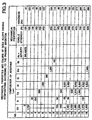
- breaking strength was measured by conducting a tensile test at ordinary temperature, and also Vickers hardness and the ball shape at bonding were observed. The results are shown in FIG.2.
- FIG. 1 shows the softening curves of small-diameter gold alloy wires (diameter: 0.8 mm) admixed with gadolinium Gd, boron B and aluminum Al.
- a high-speed automatic bonder was used to form a gold alloy ball by an arc discharge of an electric torch, and the ball shape was observed using a scanning electron microscope. A bond with a satisfactory shape is indicated by the mark " ⁇ " and a bond with a defective shape is indicated by the mark " ⁇ ".
- a lead frame and a semiconductor device to be measured were fixed by means of a jig, and a central portion of the small-diameter gold alloy wire was pulled apart to measure the tensile strength at breakage of the wire.
- very fine wires produced using the high-purity gold alloys according to the present invention have higher breaking strength, hardness and heat resistance than conventional high-purity gold alloy wires, are less subject to variations or disconnection, and permit stable bonding. Excellent electrical characteristics can also be achieved. Since the gold alloy wires of the present invention are improved especially in mechanical strength, hardness and heat resistance at ordinary temperature, tensile strength at high temperature is also high, the junction loop height can be reduced, and the gold alloy wires could be used satisfactorily in high-speed automatic bonding. Also, the ball shape was perfectly spherical and thus small, making it possible to improve the yield and reduce the cost.
- mother alloys admixed with the aforementioned elements were prepared by using 4N pure gold having a gold purity of 99.99 weight %.
- the alloys were individually melted by high-frequency vacuum melting and were cast into ingots (20 mm ⁇ 20 mm ⁇ 150 mm). Subsequently, the ingots were heated at 800°C for one hour and then rapidly cooled in water, followed by work hardening and age hardening. The working ratio was 99.5% and the aging treatment was performed at 250°C for three hours.
- the gold alloys according to the method of the present invention have a gold content of 98.5 weight % or more, have increased hardness and tensile strength as mechanical properties, and are also improved in heat resistance and color tone.
- the gold alloys showed satisfactory strength for use in dental members.
- Dental members are required to ensure biological safety, besides good mechanical properties.
- the above high-purity gold alloys have small amounts of additive elements contained therein, and thus it can be said that their degree of safety is high.
- By suitably selecting the additive elements it is possible to obtain dental members 'satisfying both the mechanical and biological requirements.
- biological safety different approval systems are adopted in different countries, and in Japan, approval by the Ministry of Welfare is required under the Pharmaceutical Affairs Law.
- High-purity gold alloys admixed with 1000 ppm of rare-earth elements and alkaline earth metals and having a gold purity of 99.9 weight % were prepared by way of experiment and the colors thereof were examined; as a result, it was found that the gold alloys admixed with Gd, La, Ce, Sm or Yb had a pure gold-like color and that among them, the gold alloy admixed with gadolinium Gd had a color most close to pure gold.
- the high-purity hard gold alloy member according to the present invention is. suitable for use as a decorative member such as a necklace, a watch, etc., an electronic member such as a bonding wire, a lead frame, a thin film, etc., and a dental member.
Landscapes
- Chemical & Material Sciences (AREA)
- Engineering & Computer Science (AREA)
- Organic Chemistry (AREA)
- Power Engineering (AREA)
- Microelectronics & Electronic Packaging (AREA)
- Materials Engineering (AREA)
- Mechanical Engineering (AREA)
- Metallurgy (AREA)
- Computer Hardware Design (AREA)
- Manufacturing & Machinery (AREA)
- Physics & Mathematics (AREA)
- Thermal Sciences (AREA)
- Crystallography & Structural Chemistry (AREA)
- Adornments (AREA)
- Conductive Materials (AREA)
- Manufacture And Refinement Of Metals (AREA)
- Dental Preparations (AREA)
- Wire Bonding (AREA)
Abstract
Description
- The present invention relates to an electronic member, a dental member and a decorative member.
- A high-purity gold alloy member as an electronic member is used to connect an electrode on a semiconductor device and an external lead and has excellent heat resistance. More specifically, the gold alloy has electrical characteristics and bonding characteristics equivalent to or superior to those of conventional gold alloys despite its small wire diameter. The high-purity gold alloy according to the present invention has good electrical characteristics and is especially excellent in mechanical strength and in breaking strength at hot working.
- Gold alloy is used in most dental members and has a low purity of gold Au ranging from 42 to 95 mass %. The present invention provides a high-purity gold alloy for dental use which has a composition of high-purity gold alloy and yet improved mechanical characteristics, and retains the characteristics specific to gold, such as corrosion resistance, color tone, etc.
- Gold alloy is expected to be pure gold-like yellow in color and bright. A hardening method according to the present invention provides a pure gold-colored, high-purity gold alloy.
- Fine wires of gold alloy are used chiefly as bonding wires for connecting electrodes on semiconductor devices and external leads. Thermocompression bonding is adopted as a bonding technique. A distal end portion of a fine alloy wire is heated and melted with the use of an electric torch to form a ball, and the ball is compression-bonded to an electrode of a semiconductor device heated at 150 to 300°C. Further, the alloy wire is bonded to an external lead by ultrasonic compression bonding.
- A trend for higher integration of semiconductor devices has created needs for shorter pitch of interelectrode distances, smaller ball diameter, longer path, etc., and thus there is a great demand for finer wires. Conventional high-purity gold alloys have low breaking strength as a mechanical strength when reduced in wire diameter and thus difficulty arises in meeting the requirements for further reduction in wire diameter. Fine wires of gold alloy with high mechanical strength and heat resistance are therefore demanded.
- Conventional high-purity gold alloys are admixed with excessive alloying elements for reduction in wire diameter, and due to oxidation of the additive elements during the formation of a ball, an oxide layer is formed on the surface of the ball, with the result that the bonding strength lowers because the ball fails to be satisfactorily bonded to an electrode at the time of thermocompression bonding. Further, since the ball has increased hardness, its deformation factor and shear strength are low at the time of compression bonding, and in extreme cases, the ball breaks the semiconductor device. Also, a shrinkage hole is liable to be formed at the extremity of the ball, and because of consequent reduction in the bonding surface, the bonding strength after the thermocompression bonding lowers.
- Gold alloys for dental applications have been in use separately for casting and working. Suitable properties vary depending on uses, and therefore, gold alloys with low to high hardness and low to high tensile strength are available on the market. Gold alloys have been considered an ideal material because they can be melted even with the use of town gas and thus are easy to cast and also they have good conformability. However, gold alloys, which are expensive, do not have high purity and satisfactory strength, and the characteristics specific to gold, such as corrosion resistance, color tone, etc., could not be fully enjoyed.
- Gold alloys having a hardness and a tensile strength as mechanical properties ranging from 80 to 280 Hv and from 350 to 1100 MPa, respectively, are used for different applications. As additives added to the alloys, those additives which have a large volume percentage and which change the color tone are mainly used. Therefore, there is a demand for additives that are small in volume percentage and can retain bright pure gold color.
- Conventional gold alloys are admixed with. Cu to increase the hardness by age hardening of the ordered lattice, with indium or rhenium to reduce the size of crystal grains, and with palladium to enhance the corrosion resistance, in such a manner that these characteristics are well-balanced.
- GB 2116208A describes an alloy consisting of 50 ppm of Gd, balance Au, and an alloy consisting of 440 ppm of Gd, balance Au.
- By admixing high-purity gold for bonding with gadolinium Gd or further with a trace amount of boron B, subjecting the alloy to solution heat treatment followed by age hardening treatment, mechanical properties, hardness and breaking strength are remarkably improved and also the recrystallization region for the formation of a ball is expanded. It was found that where a small amount of boron B coexisted with gadolinium Gd and further with Group II and Group III elements, satisfactory additive effects could be achieved (see FIG.2).
- A fine bonding wire of high-purity gold alloy capable of forming a ball neck suited for reduction in wire diameter and having small bonding grains can be obtained.
- There have been proposed gold alloy wires which are admixed with small amounts of Ca, Be, B, etc. to eliminate the drawbacks with high-purity gold wires (Unexamined Japanese Patent Publication (KOKAI) No. 53-105968, No. 53-112059 and No. 59-65440). Manufacture of very fine wires is, however, still associated with many problems to be solved.
- According to the method of the present invention, a high-purity gold alloy (Au: 99.98 % or more) for bonding has a gadolinium content ranging from from 1 ppm to 99.9 ppm by weight %, and the total amount of the additive is 199 ppm or less.
- Boron B shows low solid solubility in gold and serves to enhance mechanical strength. Adding a small amount of boron increases work hardness and tensile strength, but heat resistance is not improved. By adding gadolinium Gd, heat resistance improved and age hardening effect, work hardening effect and breaking strength could be remarkably enhanced, and also a synergistic effect was observed (see FIG.2).
- If an excessive amount of boron B is added, hardness increases and 'the amount of plastic deformation of the ball decreases, with the result that a satisfactory bonding strength is not obtained or that a fine crack is formed in the semiconductor device. Further, difficulty arises in the formation of a perfectly spherical ball. If the amount of boron added is too small, then the distribution of boron within gold becomes uneven, and consequent variations in mechanical strength lead to unstable bonding strength, making products defective.
- If the amount of gadolinium Gd added is too small, the effect of heat treatment is also small. Even if a large amount of gadolinium is added, well-balanced strength is not fully achieved unless gadolinium is used in combination with other elements.
- If an excessive amount of calcium Ca is added, a shrinkage hole is formed at the extremity of a ball and the ball formed is not perfectly spherical, lowering the bonding strength. If the Ca content is too small, on the other hand, cooperating effect and combined effect are not fully achieved. Beryllium Be, aluminum Al, antimony Sb, silicon Si and samarium Sm, when added, showed a tendency similar to that observed in the case where calcium was added.
- Adding beryllium showed an effect very similar to that achieved with calcium, and adding yttrium showed an effect closely similar to that obtained with samarium.
- Gadolinium Gd, when added in combination with a rare-earth element or an alkaline earth metal, showed a marked additive effect.
- For a gold alloy for dental use having a purity of 98.50 to 99.96 weight %, its mechanical strength, hardness, tensile strength and heat resistance could be remarkably enhanced by. adding gadolinium Gd to the gold alloy and then subjeetinq the alloy to aging by heat treatment. Articles admixed with gadolinium are small in volume and the color thereof is close to pure gold.
- If gadolinium Gd is added and then aging treatment is performed, hardness, tensile strength and heat resistance are enhanced. Where gadolinium Gd is added in combination with the aforementioned additive elements, a synergistic effect can be achieved through the admixture of gadolinium with other elements.
- Boron B can remarkably enhance the work hardness if added in a small quantity, but has low solid solubility.
- Where calcium Ca, beryllium Be, yttrium Y or samarium Sm is added, hardness by means of work hardening and heat resistance are improved.
- Silicon si, when added, improves cast ingot hardness and work hardness.
- Adding aluminum Al remarkably increases tensile strength, and also enhances work hardness. Antimony Sb serves to increase work hardness. Where these elements were added in combination with an alkaline earth metal or a rare-earth element, the above properties could be furthered.
-
- FIG. 1 shows improvements in softening curve achieved by the addition of gadolinium Gd, boron B and aluminum Al in a high-purity gold alloy according to the present invention;
- FIG. 2 shows tensile strength, Vickers hardness and ball shape of sample high-purity gold alloy wires; and
- FIG. 3 shows mechanical characteristics (tensile strength, Vickers hardness) of sample gold alloys for dental use.
-
- To obtain a high-purity gold alloy for bonding wire, mother alloys admixed with the aforementioned elements were prepared by using electrolytic gold having a gold purity of 99.995 weight %. Using a high-frequency vacuum melting furnace, the alloys were individually melted and cast into ingots of 20 mm × 20 mm × 150 mm.
- The cast ingots of high-purity gold alloys having the chemical compositions as shown in Table 1 were first rolled, then worked with the use of a grooved roll, and finally drawn at ordinary temperature to obtain a wire of 20 micrometers in diameter. As heat treatment, solution heat treatment was performed first at 800°C, followed by three hours of age hardening at 250°C.
- For the purpose of evaluation, breaking strength was measured by conducting a tensile test at ordinary temperature, and also Vickers hardness and the ball shape at bonding were observed. The results are shown in FIG.2.
- FIG. 1 shows the softening curves of small-diameter gold alloy wires (diameter: 0.8 mm) admixed with gadolinium Gd, boron B and aluminum Al.
- For the evaluation of the ball shape, a high-speed automatic bonder was used to form a gold alloy ball by an arc discharge of an electric torch, and the ball shape was observed using a scanning electron microscope. A bond with a satisfactory shape is indicated by the mark "○" and a bond with a defective shape is indicated by the mark "×".
- For the evaluation of the bonding strength, after the high-speed bonding, a lead frame and a semiconductor device to be measured were fixed by means of a jig, and a central portion of the small-diameter gold alloy wire was pulled apart to measure the tensile strength at breakage of the wire.
- In view of a trend for finer wires, very fine wires produced using the high-purity gold alloys according to the present invention have higher breaking strength, hardness and heat resistance than conventional high-purity gold alloy wires, are less subject to variations or disconnection, and permit stable bonding. Excellent electrical characteristics can also be achieved. Since the gold alloy wires of the present invention are improved especially in mechanical strength, hardness and heat resistance at ordinary temperature, tensile strength at high temperature is also high, the junction loop height can be reduced, and the gold alloy wires could be used satisfactorily in high-speed automatic bonding. Also, the ball shape was perfectly spherical and thus small, making it possible to improve the yield and reduce the cost.
- To obtain gold alloys for dental use, mother alloys admixed with the aforementioned elements were prepared by using 4N pure gold having a gold purity of 99.99 weight %. The alloys were individually melted by high-frequency vacuum melting and were cast into ingots (20 mm × 20 mm × 150 mm). Subsequently, the ingots were heated at 800°C for one hour and then rapidly cooled in water, followed by work hardening and age hardening. The working ratio was 99.5% and the aging treatment was performed at 250°C for three hours.
- Mechanical characteristics were evaluated as to Vickers hardness and tensile strength. The results are shown in FIG. 3.
- The gold alloys according to the method of the present invention have a gold content of 98.5 weight % or more, have increased hardness and tensile strength as mechanical properties, and are also improved in heat resistance and color tone. The gold alloys showed satisfactory strength for use in dental members.
- Dental members are required to ensure biological safety, besides good mechanical properties. The above high-purity gold alloys have small amounts of additive elements contained therein, and thus it can be said that their degree of safety is high. By suitably selecting the additive elements, it is possible to obtain dental members 'satisfying both the mechanical and biological requirements. As for biological safety, different approval systems are adopted in different countries, and in Japan, approval by the Ministry of Welfare is required under the Pharmaceutical Affairs Law.
- High-purity gold alloys admixed with 1000 ppm of rare-earth elements and alkaline earth metals and having a gold purity of 99.9 weight % were prepared by way of experiment and the colors thereof were examined; as a result, it was found that the gold alloys admixed with Gd, La, Ce, Sm or Yb had a pure gold-like color and that among them, the gold alloy admixed with gadolinium Gd had a color most close to pure gold.
- As described above, the high-purity hard gold alloy member according to the present invention is. suitable for use as a decorative member such as a necklace, a watch, etc., an electronic member such as a bonding wire, a lead frame, a thin film, etc., and a dental member.
Claims (5)
- A method for manufacturing a high-purity hard gold alloy comprising the steps of:providing an alloy comprising 1-99.9 ppm of Gd, optionally 0.1-150 ppm of B, optionally one or more additives selected from the group consisting of Al, Si, Y, Sb, rare-earth metals and alkaline earth metals in a total amount of 1-199 ppm, the balance being gold with a purity of 99.98 % by weight or more and incidental impurities;subjecting said alloy to solution heat treatment at a temperature higher than a solubility curve followed by rapid cooling, thereby an alloy with a uniform distribution of the components is obtained ;subjecting to age hardening treatment said alloy; andoptionally working said alloy into a desired shape, said age hardening being performed before of after said working step.
- A method for manufacturing a high-purity hard gold alloy comprising the steps of:providing an alloy comprising 50-14,999 ppm of Gd, optionally 0.1-150 ppm of B, optionally one or more additives selected from the group consisting of Al, Si, Y, Sb, rare-earth metals and alkaline earth metals in a total amount of 3001-14,999 ppm, and incidental impurities, the balance being gold with a purity of 98.5 - 99.69 % by weight;subjecting said alloy to solution heat treatment at a temperature higher than a solubility curve followed by rapid cooling, thereby an alloy with a uniform distribution of the components is obtained ;subjecting to age hardening treatment said alloy; andoptionally working said alloy into a desired shape, said age hardening being performed before of after said working step.
- The method according to claim 1 or 2, characterized in that said one or more additives are selected from the group consisting of Be, Al, Si, Ca, Sm, Y and Sb.
- The method according to claim 1 or 2, wherein said solution heat treatment is performed at a heating temperature of 600 to 2800 °C, and said age hardening treatment is performed at a temperature of 150 to 350 °C.
- The method according to any one of claim 1 through 3, wherein after said solution heat treatment, said working step and said age hardening treatment are alternatively repeated.
Applications Claiming Priority (5)
| Application Number | Priority Date | Filing Date | Title |
|---|---|---|---|
| JP18524296 | 1996-06-12 | ||
| JP18524396 | 1996-06-12 | ||
| JP18524396 | 1996-06-12 | ||
| JP18524296 | 1996-06-12 | ||
| PCT/JP1997/002014 WO1997047778A1 (en) | 1996-06-12 | 1997-06-11 | High purity hard gold alloy and method of manufacturing same |
Publications (3)
| Publication Number | Publication Date |
|---|---|
| EP0922780A1 EP0922780A1 (en) | 1999-06-16 |
| EP0922780A4 EP0922780A4 (en) | 1999-12-22 |
| EP0922780B1 true EP0922780B1 (en) | 2002-09-25 |
Family
ID=26502987
Family Applications (1)
| Application Number | Title | Priority Date | Filing Date |
|---|---|---|---|
| EP97927367A Expired - Lifetime EP0922780B1 (en) | 1996-06-12 | 1997-06-11 | Method of manufacturing a high purity hard gold alloy |
Country Status (7)
| Country | Link |
|---|---|
| US (1) | US6063213A (en) |
| EP (1) | EP0922780B1 (en) |
| CN (1) | CN1085738C (en) |
| AT (1) | ATE224961T1 (en) |
| DE (1) | DE69715885T2 (en) |
| HK (1) | HK1020998A1 (en) |
| WO (1) | WO1997047778A1 (en) |
Families Citing this family (17)
| Publication number | Priority date | Publication date | Assignee | Title |
|---|---|---|---|---|
| US6319617B1 (en) * | 1999-12-17 | 2001-11-20 | Agere Systems Gaurdian Corp. | Oxide-bondable solder |
| US6306516B1 (en) * | 1999-12-17 | 2001-10-23 | Agere Systems Guardian Corp. | Article comprising oxide-bondable solder |
| JP2001049364A (en) | 2000-07-03 | 2001-02-20 | Kazuo Ogasa | Hard noble metal alloy member and its production |
| KR100618052B1 (en) * | 2003-04-14 | 2006-08-30 | 엠케이전자 주식회사 | Au alloy bonding wire for semiconductor device |
| US20080050267A1 (en) * | 2004-09-30 | 2008-02-28 | Hiroshi Murai | Au Alloy Bonding Wire |
| US20060231171A1 (en) * | 2005-04-19 | 2006-10-19 | Davis Samuel A | Method for adding boron to metal alloys |
| US7713390B2 (en) * | 2005-05-16 | 2010-05-11 | Applied Materials, Inc. | Ground shield for a PVD chamber |
| US7224067B2 (en) * | 2005-09-15 | 2007-05-29 | Intel Corporation | Intermetallic solder with low melting point |
| US20070075430A1 (en) * | 2005-09-30 | 2007-04-05 | Daewoong Suh | Solder joint intermetallic compounds with improved ductility and toughness |
| DE102006006728A1 (en) * | 2006-02-13 | 2007-08-23 | W.C. Heraeus Gmbh | bonding wire |
| WO2008072485A1 (en) * | 2006-11-24 | 2008-06-19 | Kazuo Ogasa | High-performance elastic metal alloy member and process for production thereof |
| US9212408B2 (en) | 2007-09-19 | 2015-12-15 | Citizen Holdings Co., Ltd. | Decorative part with substrate and multi-layer hardening laminate |
| JP2012251235A (en) * | 2011-06-06 | 2012-12-20 | Three O Co Ltd | Fine crystallite high-performance metal alloy member, and manufacturing method therefor |
| CN104011235A (en) * | 2011-11-08 | 2014-08-27 | 斯沃奇集团研究和开发有限公司 | Gold Timepiece Or Jewellery Part |
| CN103695692B (en) * | 2013-12-11 | 2015-11-25 | 广州番禺职业技术学院 | A kind of high-purity high rigidity alloy material and preparation method thereof |
| JP6302780B2 (en) * | 2014-07-14 | 2018-03-28 | 株式会社グローバルコーポレーション | Method for producing 999 gold alloy and silver alloy having high hardness and high strength |
| CN111485131B (en) * | 2020-04-17 | 2021-12-24 | 烟台招金励福贵金属股份有限公司 | Gold bonding wire and preparation method thereof |
Family Cites Families (7)
| Publication number | Priority date | Publication date | Assignee | Title |
|---|---|---|---|---|
| GB2116208B (en) * | 1981-12-04 | 1985-12-04 | Mitsubishi Metal Corp | Fine gold alloy wire for bonding of a semiconductor device |
| JPS6357753A (en) * | 1986-08-29 | 1988-03-12 | Citizen Watch Co Ltd | Manufacture of personal ornaments |
| JP2641000B2 (en) * | 1991-12-26 | 1997-08-13 | 新日本製鐵株式会社 | Gold alloy fine wire for bonding |
| JP2780611B2 (en) * | 1993-09-06 | 1998-07-30 | 三菱マテリアル株式会社 | Gold decorative materials hardened by alloying small amounts of components |
| JP3221178B2 (en) * | 1993-09-06 | 2001-10-22 | 三菱マテリアル株式会社 | High hardness wire drawn wire for gold ornaments with excellent hardness stability |
| CN1084795C (en) * | 1995-04-07 | 2002-05-15 | 小笠和男 | High-purity hard gold alloy and process for production thereof |
| JP3337049B2 (en) * | 1995-05-17 | 2002-10-21 | 田中電子工業株式会社 | Gold wire for bonding |
-
1997
- 1997-06-11 DE DE69715885T patent/DE69715885T2/en not_active Expired - Fee Related
- 1997-06-11 AT AT97927367T patent/ATE224961T1/en not_active IP Right Cessation
- 1997-06-11 WO PCT/JP1997/002014 patent/WO1997047778A1/en active IP Right Grant
- 1997-06-11 CN CN97195394A patent/CN1085738C/en not_active Expired - Fee Related
- 1997-06-11 EP EP97927367A patent/EP0922780B1/en not_active Expired - Lifetime
-
1998
- 1998-12-08 US US09/216,754 patent/US6063213A/en not_active Expired - Fee Related
-
1999
- 1999-12-23 HK HK99106076A patent/HK1020998A1/en not_active IP Right Cessation
Also Published As
| Publication number | Publication date |
|---|---|
| EP0922780A4 (en) | 1999-12-22 |
| CN1085738C (en) | 2002-05-29 |
| DE69715885T2 (en) | 2003-06-05 |
| ATE224961T1 (en) | 2002-10-15 |
| DE69715885D1 (en) | 2002-10-31 |
| CN1221459A (en) | 1999-06-30 |
| HK1020998A1 (en) | 2000-05-26 |
| WO1997047778A1 (en) | 1997-12-18 |
| US6063213A (en) | 2000-05-16 |
| EP0922780A1 (en) | 1999-06-16 |
Similar Documents
| Publication | Publication Date | Title |
|---|---|---|
| EP0922780B1 (en) | Method of manufacturing a high purity hard gold alloy | |
| JPS62127438A (en) | Bonding wire for semiconductor device | |
| US6103025A (en) | Fine wire of gold alloy, method for manufacture thereof and use thereof | |
| JPH06271959A (en) | Palladium fine wire for wire bonding of semiconductor device | |
| JP2922388B2 (en) | Gold alloy fine wire for bonding | |
| JPH11222639A (en) | Extra fine wire composed of gold alloy for bringing semiconductor component into contact and its production | |
| JPS63235440A (en) | Fine copper wire and its production | |
| JPS62104061A (en) | Bonding wire for semiconductor element and manufacture thereof | |
| JP2003059964A (en) | Bonding wire and manufacturing method therefor | |
| EP1811556A1 (en) | Wire bump material | |
| KR101158547B1 (en) | Gold alloy wire for ball bonding | |
| CN110699570B (en) | High-balling-performance bonding silver wire material and preparation method thereof | |
| JPH0726167B2 (en) | Au alloy extra fine wire for bonding wire of semiconductor device | |
| JPH0464121B2 (en) | ||
| KR101047827B1 (en) | Gold Alloy Wire for Ball Bonding | |
| JPS62127437A (en) | Bonding wire for semiconductor device | |
| JP2003023030A (en) | Bonding wire and manufacturing method therefor | |
| JPS62127436A (en) | Bonding wire for semiconductor device | |
| JPS63241942A (en) | Fine copper wire and manufacture thereof | |
| JPS61110735A (en) | Cold alloy having superior heat resistance | |
| JP2766701B2 (en) | Bonding wire | |
| JPS5957441A (en) | Al alloy thin wire for wire-bonding of semiconductor device | |
| JPS63243243A (en) | Fine copper wire and its production | |
| JPS6294969A (en) | Bonding wire for semiconductor device | |
| JPH05132729A (en) | Copper bonding wire |
Legal Events
| Date | Code | Title | Description |
|---|---|---|---|
| PUAI | Public reference made under article 153(3) epc to a published international application that has entered the european phase |
Free format text: ORIGINAL CODE: 0009012 |
|
| 17P | Request for examination filed |
Effective date: 19990111 |
|
| AK | Designated contracting states |
Kind code of ref document: A1 Designated state(s): AT BE CH DE DK ES FI FR GB GR IE IT LI LU MC NL PT SE |
|
| A4 | Supplementary search report drawn up and despatched |
Effective date: 19991105 |
|
| AK | Designated contracting states |
Kind code of ref document: A4 Designated state(s): AT BE CH DE DK ES FI FR GB GR IE IT LI LU MC NL PT SE |
|
| 17Q | First examination report despatched |
Effective date: 20010116 |
|
| GRAG | Despatch of communication of intention to grant |
Free format text: ORIGINAL CODE: EPIDOS AGRA |
|
| RTI1 | Title (correction) |
Free format text: METHOD OF MANUFACTURING A HIGH PURITY HARD GOLD ALLOY |
|
| GRAG | Despatch of communication of intention to grant |
Free format text: ORIGINAL CODE: EPIDOS AGRA |
|
| GRAH | Despatch of communication of intention to grant a patent |
Free format text: ORIGINAL CODE: EPIDOS IGRA |
|
| GRAH | Despatch of communication of intention to grant a patent |
Free format text: ORIGINAL CODE: EPIDOS IGRA |
|
| GRAA | (expected) grant |
Free format text: ORIGINAL CODE: 0009210 |
|
| AK | Designated contracting states |
Kind code of ref document: B1 Designated state(s): AT BE CH DE DK ES FI FR GB GR IE IT LI LU MC NL PT SE |
|
| PG25 | Lapsed in a contracting state [announced via postgrant information from national office to epo] |
Ref country code: NL Free format text: LAPSE BECAUSE OF FAILURE TO SUBMIT A TRANSLATION OF THE DESCRIPTION OR TO PAY THE FEE WITHIN THE PRESCRIBED TIME-LIMIT Effective date: 20020925 Ref country code: IT Free format text: LAPSE BECAUSE OF FAILURE TO SUBMIT A TRANSLATION OF THE DESCRIPTION OR TO PAY THE FEE WITHIN THE PRE;WARNING: LAPSES OF ITALIAN PATENTS WITH EFFECTIVE DATE BEFORE 2007 MAY HAVE OCCURRED AT ANY TIME BEFORE 2007. THE CORRECT EFFECTIVE DATE MAY BE DIFFERENT FROM THE ONE RECORDED.SCRIBED TIME-LIMIT Effective date: 20020925 Ref country code: GR Free format text: LAPSE BECAUSE OF FAILURE TO SUBMIT A TRANSLATION OF THE DESCRIPTION OR TO PAY THE FEE WITHIN THE PRESCRIBED TIME-LIMIT Effective date: 20020925 Ref country code: FI Free format text: LAPSE BECAUSE OF FAILURE TO SUBMIT A TRANSLATION OF THE DESCRIPTION OR TO PAY THE FEE WITHIN THE PRESCRIBED TIME-LIMIT Effective date: 20020925 Ref country code: BE Free format text: LAPSE BECAUSE OF FAILURE TO SUBMIT A TRANSLATION OF THE DESCRIPTION OR TO PAY THE FEE WITHIN THE PRESCRIBED TIME-LIMIT Effective date: 20020925 Ref country code: AT Free format text: LAPSE BECAUSE OF FAILURE TO SUBMIT A TRANSLATION OF THE DESCRIPTION OR TO PAY THE FEE WITHIN THE PRESCRIBED TIME-LIMIT Effective date: 20020925 |
|
| REF | Corresponds to: |
Ref document number: 224961 Country of ref document: AT Date of ref document: 20021015 Kind code of ref document: T |
|
| REG | Reference to a national code |
Ref country code: GB Ref legal event code: FG4D |
|
| REG | Reference to a national code |
Ref country code: CH Ref legal event code: EP |
|
| REG | Reference to a national code |
Ref country code: IE Ref legal event code: FG4D |
|
| REF | Corresponds to: |
Ref document number: 69715885 Country of ref document: DE Date of ref document: 20021031 |
|
| REG | Reference to a national code |
Ref country code: CH Ref legal event code: NV Representative=s name: PATENTANWALTSBUERO EDER AG |
|
| PG25 | Lapsed in a contracting state [announced via postgrant information from national office to epo] |
Ref country code: SE Free format text: LAPSE BECAUSE OF FAILURE TO SUBMIT A TRANSLATION OF THE DESCRIPTION OR TO PAY THE FEE WITHIN THE PRESCRIBED TIME-LIMIT Effective date: 20021225 Ref country code: DK Free format text: LAPSE BECAUSE OF FAILURE TO SUBMIT A TRANSLATION OF THE DESCRIPTION OR TO PAY THE FEE WITHIN THE PRESCRIBED TIME-LIMIT Effective date: 20021225 |
|
| PG25 | Lapsed in a contracting state [announced via postgrant information from national office to epo] |
Ref country code: PT Free format text: LAPSE BECAUSE OF FAILURE TO SUBMIT A TRANSLATION OF THE DESCRIPTION OR TO PAY THE FEE WITHIN THE PRESCRIBED TIME-LIMIT Effective date: 20021226 |
|
| ET | Fr: translation filed | ||
| NLV1 | Nl: lapsed or annulled due to failure to fulfill the requirements of art. 29p and 29m of the patents act | ||
| PG25 | Lapsed in a contracting state [announced via postgrant information from national office to epo] |
Ref country code: ES Free format text: LAPSE BECAUSE OF FAILURE TO SUBMIT A TRANSLATION OF THE DESCRIPTION OR TO PAY THE FEE WITHIN THE PRESCRIBED TIME-LIMIT Effective date: 20030328 |
|
| PG25 | Lapsed in a contracting state [announced via postgrant information from national office to epo] |
Ref country code: LU Free format text: LAPSE BECAUSE OF NON-PAYMENT OF DUE FEES Effective date: 20030611 Ref country code: IE Free format text: LAPSE BECAUSE OF NON-PAYMENT OF DUE FEES Effective date: 20030611 |
|
| PG25 | Lapsed in a contracting state [announced via postgrant information from national office to epo] |
Ref country code: MC Free format text: LAPSE BECAUSE OF NON-PAYMENT OF DUE FEES Effective date: 20030630 |
|
| PLBE | No opposition filed within time limit |
Free format text: ORIGINAL CODE: 0009261 |
|
| STAA | Information on the status of an ep patent application or granted ep patent |
Free format text: STATUS: NO OPPOSITION FILED WITHIN TIME LIMIT |
|
| 26N | No opposition filed |
Effective date: 20030626 |
|
| REG | Reference to a national code |
Ref country code: IE Ref legal event code: MM4A |
|
| PGFP | Annual fee paid to national office [announced via postgrant information from national office to epo] |
Ref country code: FR Payment date: 20040607 Year of fee payment: 8 Ref country code: CH Payment date: 20040607 Year of fee payment: 8 |
|
| PG25 | Lapsed in a contracting state [announced via postgrant information from national office to epo] |
Ref country code: LI Free format text: LAPSE BECAUSE OF NON-PAYMENT OF DUE FEES Effective date: 20050630 Ref country code: CH Free format text: LAPSE BECAUSE OF NON-PAYMENT OF DUE FEES Effective date: 20050630 |
|
| REG | Reference to a national code |
Ref country code: CH Ref legal event code: PL |
|
| PG25 | Lapsed in a contracting state [announced via postgrant information from national office to epo] |
Ref country code: FR Free format text: LAPSE BECAUSE OF NON-PAYMENT OF DUE FEES Effective date: 20060228 |
|
| REG | Reference to a national code |
Ref country code: FR Ref legal event code: ST Effective date: 20060228 |
|
| PGFP | Annual fee paid to national office [announced via postgrant information from national office to epo] |
Ref country code: DE Payment date: 20060614 Year of fee payment: 10 |
|
| PGFP | Annual fee paid to national office [announced via postgrant information from national office to epo] |
Ref country code: GB Payment date: 20060620 Year of fee payment: 10 |
|
| REG | Reference to a national code |
Ref country code: HK Ref legal event code: WD Ref document number: 1021996 Country of ref document: HK |
|
| GBPC | Gb: european patent ceased through non-payment of renewal fee |
Effective date: 20070611 |
|
| PG25 | Lapsed in a contracting state [announced via postgrant information from national office to epo] |
Ref country code: DE Free format text: LAPSE BECAUSE OF NON-PAYMENT OF DUE FEES Effective date: 20080101 |
|
| PG25 | Lapsed in a contracting state [announced via postgrant information from national office to epo] |
Ref country code: GB Free format text: LAPSE BECAUSE OF NON-PAYMENT OF DUE FEES Effective date: 20070611 |