EP0920090A2 - Connecteur de circuit imprimé - Google Patents
Connecteur de circuit imprimé Download PDFInfo
- Publication number
- EP0920090A2 EP0920090A2 EP98121557A EP98121557A EP0920090A2 EP 0920090 A2 EP0920090 A2 EP 0920090A2 EP 98121557 A EP98121557 A EP 98121557A EP 98121557 A EP98121557 A EP 98121557A EP 0920090 A2 EP0920090 A2 EP 0920090A2
- Authority
- EP
- European Patent Office
- Prior art keywords
- connector
- springs
- circuit
- pads
- cover
- Prior art date
- Legal status (The legal status is an assumption and is not a legal conclusion. Google has not performed a legal analysis and makes no representation as to the accuracy of the status listed.)
- Withdrawn
Links
Images


Classifications
-
- H—ELECTRICITY
- H01—ELECTRIC ELEMENTS
- H01R—ELECTRICALLY-CONDUCTIVE CONNECTIONS; STRUCTURAL ASSOCIATIONS OF A PLURALITY OF MUTUALLY-INSULATED ELECTRICAL CONNECTING ELEMENTS; COUPLING DEVICES; CURRENT COLLECTORS
- H01R12/00—Structural associations of a plurality of mutually-insulated electrical connecting elements, specially adapted for printed circuits, e.g. printed circuit boards [PCB], flat or ribbon cables, or like generally planar structures, e.g. terminal strips, terminal blocks; Coupling devices specially adapted for printed circuits, flat or ribbon cables, or like generally planar structures; Terminals specially adapted for contact with, or insertion into, printed circuits, flat or ribbon cables, or like generally planar structures
- H01R12/70—Coupling devices
- H01R12/71—Coupling devices for rigid printing circuits or like structures
- H01R12/72—Coupling devices for rigid printing circuits or like structures coupling with the edge of the rigid printed circuits or like structures
- H01R12/721—Coupling devices for rigid printing circuits or like structures coupling with the edge of the rigid printed circuits or like structures cooperating directly with the edge of the rigid printed circuits
-
- H—ELECTRICITY
- H01—ELECTRIC ELEMENTS
- H01R—ELECTRICALLY-CONDUCTIVE CONNECTIONS; STRUCTURAL ASSOCIATIONS OF A PLURALITY OF MUTUALLY-INSULATED ELECTRICAL CONNECTING ELEMENTS; COUPLING DEVICES; CURRENT COLLECTORS
- H01R12/00—Structural associations of a plurality of mutually-insulated electrical connecting elements, specially adapted for printed circuits, e.g. printed circuit boards [PCB], flat or ribbon cables, or like generally planar structures, e.g. terminal strips, terminal blocks; Coupling devices specially adapted for printed circuits, flat or ribbon cables, or like generally planar structures; Terminals specially adapted for contact with, or insertion into, printed circuits, flat or ribbon cables, or like generally planar structures
- H01R12/70—Coupling devices
- H01R12/77—Coupling devices for flexible printed circuits, flat or ribbon cables or like structures
- H01R12/79—Coupling devices for flexible printed circuits, flat or ribbon cables or like structures connecting to rigid printed circuits or like structures
-
- H—ELECTRICITY
- H05—ELECTRIC TECHNIQUES NOT OTHERWISE PROVIDED FOR
- H05K—PRINTED CIRCUITS; CASINGS OR CONSTRUCTIONAL DETAILS OF ELECTRIC APPARATUS; MANUFACTURE OF ASSEMBLAGES OF ELECTRICAL COMPONENTS
- H05K3/00—Apparatus or processes for manufacturing printed circuits
- H05K3/36—Assembling printed circuits with other printed circuits
- H05K3/361—Assembling flexible printed circuits with other printed circuits
- H05K3/365—Assembling flexible printed circuits with other printed circuits by abutting, i.e. without alloying process
Definitions
- the present invention relates in general to electrical connectors. More particularly, the present invention relates to a structure for releasably connecting contacts of a circuit to conductive pads on a printed circuit board.
- PCB printed circuit board
- a connector mounted to one or both ends of the jumper, is formed with a set of electrical receptacles or sockets which is designed to receive the terminal posts or contact the pads on the PCB.
- a primary focus of manufacturers is to increase the circuit density associated with interconnecting the sub-assemblies and components found within their products. This leads to higher density modules, each requiring multiple interconnections to other modules.
- major problems with connectors having closely spaced contacts include the problems of cross-talk, lack of controlled impedance, and increased inductance.
- the present invention provides a structure for releasably connecting contacts of a circuit to conductive pads on a circuit board that reduces cross-talk, controls impedance, and reduces inductance as connector density increases.
- the present invention is directed to a connector for connecting respective electrical conductor areas of a plurality of flexible circuits with associated conductor pads of an edge connector portion of a circuit board, comprising: a connector housing having a circuit board opening sized to at least partially accommodate the edge connector portion, and a further opening allowing passage of the flexible circuits into an interior cavity of the connector housing; a first spring having a resilient arched feature for supporting one of the flexible circuits to resiliently bias an electrical conductor area of the flexible circuit into electrical contact with associated conductor pads when the connector engages the edge connector portion; and a second spring having a resilient arched feature for supporting another of the flexible circuits to resiliently bias an electrical conductor area of the another flexible circuit into electrical contact with associated conductor pads when the connector engages the edge connector portion, the electrical conductor area of the another flexible circuit facing the electrical conductor area of the first flexible circuit.
- At least one of the springs is bent so as to have a first L shaped portion and a second L shaped portion at an end thereof, the second L shaped portion being oriented approximately 90 degrees offset to the first L shaped portion, one end of the first L shaped portion contacting one end of the second L shaped portion.
- the springs resiliently urge the flexible circuits to provide electrical contact with the conductor pads of the edge connector portion when the connector is attached at a desired location to the circuit board.
- the connector housing comprises: a cover; a first insertion portion connected to the cover, the first insertion portion supporting the first spring; a second insertion portion connected to the first insertion portion to form the circuit board opening and the further opening, the second insertion portion supporting the second spring; and a base connected to the first and second insertion portions.
- the first and second insertion portions comprise compression support lead frames.
- the cover, the first and second insertion portions, and the base have resilient snap connector features to engage and retain the cover, the first and second insertion portions, and the base together as a unit in desired positions relative to one another.
- the cover, the first and second insertion portions, and the base have alignment features to facilitate desired registration with each other.
- the edge connector portion has a further conductor pad
- the connector further comprises: a third spring for resiliently biasing an electrical conductor area of a further flexible circuit into electrical contact with the further conductor pad when the connector engages the edge connector portion, the third spring having a resilient arched feature; and the third spring supporting the further flexible circuit to resiliently urge the further flexible circuit to provide electrical contact with the further conductor pad of the edge connector portion when the connector is attached at a desired location to the circuit board.
- the connector housing comprises: a cover; a first insertion portion connected to the cover, the first insertion portion supporting the first spring; a second insertion portion connected to the first insertion portion to form the circuit board opening and the further opening, the second insertion portion supporting the second spring; and a base connected to the first and second insertion portions, the base supporting the third spring.
- a connector for electrically conductive connection to a row of electrically conductive contact pads of a circuit comprises: a rigid housing; a flexible circuit housed, at least in part, in the housing, and having an end portion defining a row of conductive contact areas on one face thereof corresponding to the row of electrically conductive contact pads; spring means held captive by the housing, the spring means having a resilient arched feature and being bent so as to have a first L shaped portion and a second L shaped portion at an end thereof, the second L shaped portion being oriented approximately 90 degrees offset to the first L shaped portion, one end of the first L shaped portion contacting one end of the second L shaped portion; and means for attaching the flexible circuit to the spring means so that the contact areas are resiliently urged by the arched feature into electrically conductive contact with the pads when the connector is attached at a desired location to the circuit.
- the connector is for connection to an edge portion of the circuit, the edge portion having opposed faces each carrying a row of the electrically conductive contact pads, wherein the housing houses a separate spring means associated with each the row of pads; each the spring means includes a first plurality of springs each having an arched portion and each corresponding to at least one the contact area; and a separate flexible circuit is provided for each row of pads, each located and resiliently urged in the same manner.
- the arched portions of the first plurality of springs of the separate spring means are arched toward one another and the contact areas of the separate flexible circuits face one another within the housing.
- the first plurality of springs are housed in the housing and the spring means includes a second plurality of springs which extend from the housing each corresponding to a contact area of another flexible circuit; the contact areas of the another flexible circuit are positioned to be resiliently urged by the second plurality of springs into contact with a secondary row of conductive contact areas on the circuit, when the connector is attached to the circuit.
- the first and second pluralities of springs are separate and the springs of the second plurality of springs each include an arched portion positioned to provide the resilient urging of the contact areas of the another flexible circuit into conductive contact with the secondary row of conductive contact areas on the circuit.
- the housing has an opening for locating and receiving an edge portion of the circuit carrying the contact pads in a row extending along the edge portion and the contact areas of the flexible circuit electrically conductively contact the pads when the edge portion is inserted into the opening.
- the spring means includes a first plurality of parallel springs each having an arched feature and each corresponding to at least one contact area of the row of conductive contact areas.
- the housing comprises: a cover; a first insertion portion connected to the cover, the first insertion portion supporting one row of springs of the parallel springs; a second insertion portion connected to the first insertion portion to form a circuit opening, the second insertion portion supporting the other row of springs of the parallel springs; and a base connected to the first and second insertion portions.
- the cover, the first and second insertion portions, and the base have resilient snap connector features to engage and retain the cover, the first and second insertion portions, and the base together as a unit in desired positions relative to one another.
- the cover, the first and second insertion portions, and the base have alignment features to facilitate desired registration with each other.
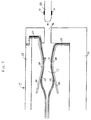
- Fig. 1 shows a cross-sectional view of an exemplary connector 10 in accordance with the present invention.
- the connector 10 comprises a molded plastic housing consisting of first and second housing halves 12 and 14.
- the housing halves 12 and 14 are spaced apart by an insulating spacer (not shown) and joined together by a support ring (not shown) to form the housing.
- the internal components of the connector 10 consist of a pair of spring means 20 and 30 and a pair of flexible circuits 23 and 33.
- the spring means and flexible circuits are inserted so that free ends 27 and 37 are secured against wall portions of the housing.
- Fig. 1 shows one pair of spring means 20 and 30, a plurality of pairs of spring means can be arranged in parallel with each other in a row to provide a plurality of contacts within the connector, as described below with respect to Fig. 8A.
- Each circuit 23, 33 comprises a flexible substrate carrying at least one, and typically a plurality of, electrical conductors terminating in electrically conductive circuit areas 25 and 35 towards an end portion of the flexible circuit within the connector 10.
- the circuit areas 25 and 35 are positioned to connect with electrically conductive pads 51 on a substrate 50 of a printed circuit board (PCB) when the connector 10 is attached to an edge connector portion of the PCB.
- PCB printed circuit board
- a PCB carries an array of circuit paths terminating at an edge connector portion in a row of electrically conductive pads 51.
- a similar row of pads is located on the underside of the PCB with the two rows being superimposed as a mirror image of one another.
- the edge connector portion containing the electrically conductive pads 51 is inserted into the edge connector receiving aperture 16 of the housing, with each electrically conductive pad 51 contacting a different spring means in the connector.
- pads shall be construed to include exposed conductors to which electrical connection is desired.
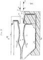
- the flexible circuits 23 and 33 extend into a cavity 17 of the housing so that the areas 25 and 35 of the flexible circuit align with the pads 51 of the PCB when the edge connector portion of the PCB is inserted into the connector through the edge connector receiving aperture 16 of the housing.
- the flexible circuits 23 and 33 are spaced apart by a spacer (not shown) with their contact areas 25 and 35 facing one another, and are biased towards one another by arched portions 28 and 38 of the spring means 20 and 30.
- the arched portions 28 and 38 are located in the housing and overlap the aperture 17 to resiliently bias the contact areas 25 and 35 of the flexible circuits 23 and 33 into engagement with pads 51 of a PCB to which the connector is attached.
- Each spring means 20 and 30 is a metal structure, and preferably is a comb-like metal structure in which, when more than one pair of spring means is present to contact a plurality of pads arranged in a row on a PCB, the arched portions are formed in parallel portions and interconnected at one end thereof by a cross-member 5, as shown for example in Fig. 2A.
- the cross-member 5 serves to maintain the spring portions in parallel alignment with one another and to locate the spring means relative to the contact areas 25 and 35 of the flexible circuit 23 and 33 and the cavity 17 of the housing.
- the ends of each spring means are shaped to define tabs which engage corresponding openings in the end portion of the associated flexible circuit to locate the flexible circuit relative to the spring.
- the spring means are stamped and formed to have a preloaded spring rate designed to provide the desired normal force at the respective contact surface with the PCB is fully engaged in the connector.
- the spring means 20, 30 are preferably made from phosphor bronze or other materials having the desired spring characteristics to provide the sufficient normal force.
- the materials selected and the geometric configuration of the spring means is preferably such that a sufficient normal force is generated at the respective contact areas to assure electrical reliability of the interconnections.
- the spring means 20 preferably has a first L shaped portion 26 and a second L shaped portion 29 at an end thereof.
- the second L shaped portion 29 is oriented approximately 90 degrees offset to the first L shaped portion 26, and one end of the first L shaped portion 26 contacts one end of the second L shaped portion 29.
- This structure provides additional strength to the connector 10 by distributing internal stresses in an optimal manner.
- the housing half 12 is formed with a groove or slot to accommodate the L shaped portions 26, 29.
- the ends of the flexible circuits 23, 33 which are remote from the connector described may be terminated in any conventional manner or may be terminated in a similar connector to that described.
- the engagement of the springs with their attached flexible circuits ensures that the free ends of the springs and the associated end portions of the flexible circuits 23, 33 do not interfere with the insertion of an edge connector portion of a PCB to the connector.
- the free end portions of the springs and the cross-member 5 serve to provide the contact with the first and second housing halves 12 and 14 required for the application of the desired spring force by the arched portion of the spring to achieve the desired electrical contact between the contact areas and the pads.
- the spring means 20, 30 may be constructed of a material or coated with a suitable material to provide, with the substrate of the flexible circuits, an impedance desired where the flexible circuit communicates directly with a PCB.
- the connector 40 of Fig. 3 includes elements similar to those described above and construction features which function substantially in the same way as the features of the embodiment described above with respect to Figs. 1 and 2 for connection to an edge connector portion of a PCB carrying rows of pads as described above. These elements are labeled identically and their description is omitted for brevity.
- the connector 40 of Fig. 3 has an additional spring means 41 and a flexible circuit 43 as shown in Fig. 4.
- the flexible circuit 43 is coupled to the spring means at an end portion of the spring 41 by a conventional means, preferably soldering.
- the flexible circuit 43 terminates at an end in electrically conductive area 45.
- Electrically conductive area 45 is positioned to connect with a secondary set of electrically conductive pads 52 of a PCB when the connector 40 is attached to the edge connector portion of the PCB.
- the secondary pads 52 are preferably positioned behind the pads 51.
- the additional spring means 41 and flexible circuit 43 can be used to contact additional voltage and signal connections in the PCB.
- the spring means 41 is a metal structure, and preferably is a comb-like metal structure in which, when more than one spring means is present to contact a plurality of pads arranged in a row on a PCB, the arched portions are formed in parallel portions and interconnected at one end thereof by a cross-member, as described above with respect to Fig. 2A.
- the cross-member maintains the spring portions in parallel alignment with one another and to locate the spring means relative to the contact area 45. Sufficient floating movement of the springs is desired to allow the desired alignment between the contact areas 45 and the pads 52 of the PCB.
- a supporting block 47 contains the spring means 41, the flexible circuit 43, and contact areas 45 in a predetermined pitch, preferably 1 mm, and is attached to a secondary plane, preferably copper, by conventional means, including soldering. It should be understood that the present invention can have any suitable pitch between contacts, as tolerances allow.
- This subassembly is inserted into the main housing and retained by retaining means 60, as shown in Fig. 5.
- the retaining means 60 preferably comprises plastic and is used for providing additional support to spring means 41 and flexible circuit 43.
- Retaining means 60 replaces housing half 14 of Fig. 1, as described below with respect to Fig. 8A.
- Fig. 6 is a cross-sectional view of another exemplary connector 70 in accordance with the present invention.
- the connector of Fig. 6 contains elements similar to those described above with respect to Figs. 1 and 3. These elements are labeled identically and their description is omitted for brevity.
- the exemplary connector 70 is similar to that shown in Fig. 3; however, in this embodiment, spring means 30 is replaced by spring means 80 that is substantially identical to spring means 20.
- the spring means 80 has a first L shaped portion 86 and a second L shaped portion 89 at an end thereof.
- the second L shaped portion 89 is oriented approximately 90 degrees offset to the first L shaped portion 86, and one end of the first L shaped portion 86 contacts one end of the second L shaped portion 89.
- This structure provides additional strength to the connector 70 by distributing internal stresses in an optimal manner.
- the supporting block 47 is formed with a groove or slot to accommodate end portion of the spring means 80. In this manner, additional strength is provided to the connector
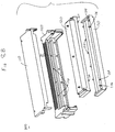
- Fig. 7 is a cross-sectional view of an exemplary connector similar to the connector shown in Fig. 6.
- the connector of Fig. 7 is shown inverted with respect to the orientation of Fig. 6 and is contained within a housing 100.
- the housing 100 comprises a cover 110, a first insertion portion 120, a second insertion portion 130, and a base 140.
- the insertion portions 120 and 130 are compression support lead frames which connect together to form a slot entry for a PCB to be inserted.
- the housing is made of plastic.
- the cover 110 corresponds to retaining means 60 of Fig. 5.
- the insertion portions 120 and 130 are used to provide support to the spring means 20 and 80 and their associated flexible circuits.
- the base 140 is used to provide support to the additional spring means 41.
- Various holes and pins corresponding to connection points between the various components are shown in dashed lines.
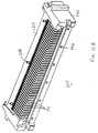
- Figs. 8A and 8B show front and rear exploded perspective views, respectively, of the housing 100.
- a plurality of the spring means can be formed in parallel alignment with one another to contact a plurality of pads on a PCB.
- a plurality of conductors (preferably copper) are spaced apart to keep the impedance and inductance low.
- Figs. 8A and 8B show a row of the additional spring means 141 (the pair of spring means 20 and 80 from Fig. 7 is not shown). The conductors come into intimate contact with pads on the substrate of the PCB.
- the base 140 has two rows of slots or holes 142 which are used as connection points for insertion portions 120 and 130. Specifically, pins 122 on insertion portion 120 and pins 132 on insertion portion 130 are press-fit or inserted through the respective rows of holes on the base 140 to provide additional support to the connector.
- the insertion portions 120 and 130 have pins and openings for connection to each other. Specifically, insertion portion 120 has pins 124 on its underside for insertion into openings 134 on insertion portion 130. Insertion portion 130 has pins 136 for insertion into openings 126 on insertion portion 120 (as shown in a bottom perspective view of the insertion portion 120 in Fig. 9).
- Figs. 10A through 10D are different views of the cover 110.
- Fig. 10A is a top view.
- Fig. 10B is a front side view.
- Fig. 10C is a bottom view.
- Fig. 10D is a perspective bottom view.
- the insertion portion 120 has pins 128 on its upper surface for insertion into openings 118 in the cover 110, as shown in Fig. 10D.
- the cover 110 has tabs 112 that are used to fasten the cover 110 to the base 140.
- any conventional fastening or fixing means including screws and adhesives, can be used to join the components of the housing 100 to one another.
- Figs. 11A and 11B show an assembled housing 100, with and without the cover 110, respectively.
- the cover 110 is attached to the base 140 by the tabs 112 or other conventional means.
- Fig. 12 is a perspective front view of an exemplary connector enclosed in a housing shown with a portion of a printed circuit 210 having an edge connector portion 220 carrying a plurality of electrically conductive contact pads 230.
- Flexible circuits 150 and 155 correspond to the flexible circuits that are coupled to the spring means that contact the primary PCB pads (e.g., flexible circuits 23 and 33 in Fig. 3).
- Flexible circuit 160 corresponds to the flexible circuit that is coupled to the spring means and contacts the secondary PCB pads (e.g., flexible circuit 43 in Fig. 3).
- the ends of the flexible circuits 150, 155, and 160 that are not coupled to the spring means can be connected to, for example, a multi-chip module.
- an exemplary connector in accordance with the present invention together with a second similar connector can be used to interconnect two PCBs, each having edge connector portions carrying rows of electrically conductive contact pads on both faces of each edge portion with the interconnection being by direct communication with contact areas at the ends of the flexible circuits which are common to the connectors.
Applications Claiming Priority (2)
| Application Number | Priority Date | Filing Date | Title |
|---|---|---|---|
| US979766 | 1992-11-20 | ||
| US08/979,766 US5971806A (en) | 1997-11-26 | 1997-11-26 | Electrical connector for connecting conductor areas of a flexible circuit with associated conductor pads of a circuit board |
Publications (2)
| Publication Number | Publication Date |
|---|---|
| EP0920090A2 true EP0920090A2 (fr) | 1999-06-02 |
| EP0920090A3 EP0920090A3 (fr) | 1999-12-15 |
Family
ID=25527144
Family Applications (1)
| Application Number | Title | Priority Date | Filing Date |
|---|---|---|---|
| EP98121557A Withdrawn EP0920090A3 (fr) | 1997-11-26 | 1998-11-18 | Connecteur de circuit imprimé |
Country Status (4)
| Country | Link |
|---|---|
| US (1) | US5971806A (fr) |
| EP (1) | EP0920090A3 (fr) |
| JP (1) | JPH11224748A (fr) |
| TW (1) | TW395588U (fr) |
Cited By (1)
| Publication number | Priority date | Publication date | Assignee | Title |
|---|---|---|---|---|
| WO2012107314A1 (fr) * | 2011-02-09 | 2012-08-16 | Robert Bosch Gmbh | Connexion enfichable permettant la mise en contact directe d'une carte de circuit imprimé |
Families Citing this family (25)
| Publication number | Priority date | Publication date | Assignee | Title |
|---|---|---|---|---|
| US6923681B1 (en) * | 1998-05-22 | 2005-08-02 | Raytheon Company | Electrical assembly for solderless interconnection of circuit boards in a stacked configuration |
| US6346012B1 (en) * | 1998-08-15 | 2002-02-12 | Delta Electronics, Inc. | Locking cartridge for conveniently locking very thin connector with near-zero inductance onto PC board |
| US6336816B1 (en) * | 2000-07-19 | 2002-01-08 | Cray Inc. | Electrical circuit connector with support |
| US6699395B1 (en) | 2000-10-18 | 2004-03-02 | Storage Technology Corporation | Method of forming alignment features for conductive devices |
| US6431876B1 (en) | 2000-10-18 | 2002-08-13 | Storage Technology Corporation | Conductive trace interconnection |
| US6641408B1 (en) | 2000-10-18 | 2003-11-04 | Storage Technology Corporation | Compliant contacts for conductive devices |
| US6508674B1 (en) | 2000-10-18 | 2003-01-21 | Storage Technology Corporation | Multi-layer conductive device interconnection |
| US6783926B2 (en) * | 2001-09-15 | 2004-08-31 | Kenneth Reece | Circuit board IC card connector |
| JP2003142183A (ja) * | 2001-11-01 | 2003-05-16 | Fujitsu Component Ltd | コンタクトモジュール、コネクタおよびコンタクトモジュールの製造方法 |
| DE10203150A1 (de) * | 2002-01-28 | 2003-07-31 | Harting Electro Optics Gmbh & | Steckverbinder mit verschiebbaren Kontaktelementen |
| DE20310734U1 (de) * | 2003-07-12 | 2003-10-23 | Harting Electro Optics Gmbh & | Steckvorrichtung zur Verbindung von Leiterplatten |
| DE102004008014A1 (de) * | 2004-02-19 | 2005-09-08 | Robert Bosch Gmbh | Direktsteckverbindung mit Kabelendhülse |
| US7172465B2 (en) * | 2005-02-22 | 2007-02-06 | Micron Technology, Inc. | Edge connector including internal layer contact, printed circuit board and electronic module incorporating same |
| US7300303B2 (en) * | 2005-09-26 | 2007-11-27 | Intel Corporation | Method and apparatus for attaching flexible circuit to a rigid printed circuit board |
| JP4762690B2 (ja) * | 2005-11-17 | 2011-08-31 | 古河電気工業株式会社 | 電気接続箱 |
| CN101584089B (zh) | 2006-12-13 | 2012-06-13 | 泛达公司 | 具有分层的插头接口触头的通信插座 |
| US20100227482A1 (en) * | 2009-03-09 | 2010-09-09 | Tyco Electronics Corporation | Mechanically supported contact and electrical connector utilizing the same |
| US8282420B2 (en) * | 2009-09-21 | 2012-10-09 | International Business Machines Corporation | Delayed contact action connector |
| US9184521B2 (en) * | 2013-09-04 | 2015-11-10 | Htc Corporation | Connector assembly and electronic device |
| US10852784B2 (en) | 2018-04-11 | 2020-12-01 | Dell Products, Lp | Relative height adjustable connector system for motherboard to graphics board transition in information handling systems |
| US10852783B2 (en) | 2018-04-11 | 2020-12-01 | Dell Products, Lp | Relative height adjustable connector system for motherboard to graphics board transition with a plating alternative in information handling systems |
| US10649505B2 (en) | 2018-04-11 | 2020-05-12 | Dell Products, Lp | Adaptable graphics board with a reconfigurable I/O module board for use in information handling systems |
| US10254793B1 (en) | 2018-04-11 | 2019-04-09 | Dell Products, Lp | Adaptable graphics board form factor with adjacent orientation to a motherboard for use with plural external I/O requirements in information handling systems |
| TWI710168B (zh) | 2020-01-21 | 2020-11-11 | 大陸商東莞立訊技術有限公司 | 連接器 |
| DE102020133073A1 (de) * | 2020-12-11 | 2022-06-15 | HELLA GmbH & Co. KGaA | Vorrichtung mit einem Gehäuse, mit einer elektrischen Schaltung in dem Gehäuse und mit einer elektrisch leitenden Verbindung zwischen dem Gehäuse und der Schaltung |
Citations (4)
| Publication number | Priority date | Publication date | Assignee | Title |
|---|---|---|---|---|
| EP0284012A2 (fr) * | 1987-03-26 | 1988-09-28 | Miraco, Inc. | Système de connexion pour plaques à circuits imprimés |
| US5240420A (en) * | 1992-03-31 | 1993-08-31 | Research Organization For Circuit Knowledge | Self-aligning high-density printed circuit connector |
| US5350319A (en) * | 1993-04-02 | 1994-09-27 | Miraco, Inc. | High-density printed circuit connector |
| US5421738A (en) * | 1994-06-29 | 1995-06-06 | Miraco, Inc. | High-density printed circuit connector with pivotable spring |
Family Cites Families (17)
| Publication number | Priority date | Publication date | Assignee | Title |
|---|---|---|---|---|
| US3334325A (en) * | 1964-11-04 | 1967-08-01 | Hughes Aircraft Co | Reference plane card connector system |
| US3407379A (en) * | 1966-05-11 | 1968-10-22 | Taiyo Yuden Kabushikikaisha | Multi-connector |
| GB1245493A (en) * | 1968-03-11 | 1971-09-08 | Texas Instruments Inc | Connector |
| DE1802130A1 (de) * | 1968-10-09 | 1970-04-23 | Siemens Ag | Vielfachstecker |
| US4613193A (en) * | 1984-08-13 | 1986-09-23 | Tritec, Inc. | Board-operated electrical connector for printed circuit boards |
| US4659155A (en) * | 1985-11-19 | 1987-04-21 | Teradyne, Inc. | Backplane-daughter board connector |
| US4911387A (en) * | 1988-06-27 | 1990-03-27 | Creative Systems Engineering, Inc. | Modular conduit system |
| US4911643A (en) * | 1988-10-11 | 1990-03-27 | Beta Phase, Inc. | High density and high signal integrity connector |
| US4938702A (en) * | 1989-09-22 | 1990-07-03 | Key Tronic Corporation | Connector clamp for attaching flat electrical conductor leads to printed wiring boards |
| US5051099A (en) * | 1990-01-10 | 1991-09-24 | Amp Incorporated | High speed card edge connector |
| US5024609A (en) * | 1990-04-04 | 1991-06-18 | Burndy Corporation | High-density bi-level card edge connector and method of making the same |
| US5076803A (en) * | 1991-02-22 | 1991-12-31 | Miraco, Inc. | Locking connector assembly |
| US5507651A (en) * | 1991-04-22 | 1996-04-16 | Kel Corporation | Connector assembly for film circuitry |
| DE69230913T2 (de) * | 1991-07-16 | 2000-12-07 | Berg Electronics Mfg | Flachbau-, oberflächenmontierter Steckverbinder mit gekrümmten freitragendenKontaktfedern. |
| US5239748A (en) * | 1992-07-24 | 1993-08-31 | Micro Control Company | Method of making high density connector for burn-in boards |
| US5496180A (en) * | 1994-04-06 | 1996-03-05 | The Whitaker Corporation | Surface mountable card edge connector |
| US5639265A (en) * | 1994-07-30 | 1997-06-17 | Mitsumi Electric Co., Ltd. | Electric connector |
-
1997
- 1997-11-26 US US08/979,766 patent/US5971806A/en not_active Expired - Fee Related
-
1998
- 1998-11-16 TW TW087218945U patent/TW395588U/zh unknown
- 1998-11-18 EP EP98121557A patent/EP0920090A3/fr not_active Withdrawn
- 1998-11-25 JP JP10334366A patent/JPH11224748A/ja active Pending
Patent Citations (4)
| Publication number | Priority date | Publication date | Assignee | Title |
|---|---|---|---|---|
| EP0284012A2 (fr) * | 1987-03-26 | 1988-09-28 | Miraco, Inc. | Système de connexion pour plaques à circuits imprimés |
| US5240420A (en) * | 1992-03-31 | 1993-08-31 | Research Organization For Circuit Knowledge | Self-aligning high-density printed circuit connector |
| US5350319A (en) * | 1993-04-02 | 1994-09-27 | Miraco, Inc. | High-density printed circuit connector |
| US5421738A (en) * | 1994-06-29 | 1995-06-06 | Miraco, Inc. | High-density printed circuit connector with pivotable spring |
Cited By (3)
| Publication number | Priority date | Publication date | Assignee | Title |
|---|---|---|---|---|
| WO2012107314A1 (fr) * | 2011-02-09 | 2012-08-16 | Robert Bosch Gmbh | Connexion enfichable permettant la mise en contact directe d'une carte de circuit imprimé |
| CN103339803A (zh) * | 2011-02-09 | 2013-10-02 | 罗伯特·博世有限公司 | 用于直接电接触印刷电路板的插塞连接 |
| CN103339803B (zh) * | 2011-02-09 | 2017-03-22 | 罗伯特·博世有限公司 | 用于直接电接触印刷电路板的插塞连接 |
Also Published As
| Publication number | Publication date |
|---|---|
| EP0920090A3 (fr) | 1999-12-15 |
| TW395588U (en) | 2000-06-21 |
| JPH11224748A (ja) | 1999-08-17 |
| US5971806A (en) | 1999-10-26 |
Similar Documents
| Publication | Publication Date | Title |
|---|---|---|
| US5971806A (en) | Electrical connector for connecting conductor areas of a flexible circuit with associated conductor pads of a circuit board | |
| US6203328B1 (en) | Connector for engaging end region of circuit substrate | |
| US6527588B2 (en) | Electrical connector with integrated PCB assembly | |
| US6540522B2 (en) | Electrical connector assembly for orthogonally mating circuit boards | |
| US6435882B1 (en) | Socketable flexible circuit based electronic device module and a socket for the same | |
| US7147481B2 (en) | Shielded electrical connector with anti-mismatching means | |
| US5399105A (en) | Conductive shroud for electrical connectors | |
| EP0632933B1 (fr) | Systeme de raccordement coaxial miniaturise a haute densite comprenant des modules de groupage positionnes en quinconce | |
| JP3035291B2 (ja) | 高速バックプレ―ン・コネクタ | |
| EP1107387A1 (fr) | Connecteur blindé | |
| EP1058352B1 (fr) | Connecteur électrique | |
| CA2248712A1 (fr) | Agencement de connecteur haute densite, destine a un module pour cartes imprimees | |
| CN1964142A (zh) | 电转接器及其组件 | |
| US3868162A (en) | Electrical connector | |
| JPH06223895A (ja) | コネクタおよびその方法 | |
| US7059907B2 (en) | Modular electrical connector | |
| CN111952806A (zh) | 直接配合电缆组件 | |
| US5895281A (en) | High density board to board connector | |
| US4629267A (en) | Circuit terminating device | |
| US7153144B2 (en) | Module connector | |
| EP0643448B1 (fr) | Connecteur coaxial pour la connexion de plaquettes de circuits imprimés | |
| EP1209764A1 (fr) | Connecteur BGA avec soulagement de contrainte | |
| KR100790762B1 (ko) | 케이블 커넥터 및 그 조립용 키트 | |
| WO2022193996A1 (fr) | Connecteur, dispositif photoélectrique et dispositif de réseau | |
| US5795184A (en) | Device for interconnecting stacked connectors and board |
Legal Events
| Date | Code | Title | Description |
|---|---|---|---|
| PUAI | Public reference made under article 153(3) epc to a published international application that has entered the european phase |
Free format text: ORIGINAL CODE: 0009012 |
|
| AK | Designated contracting states |
Kind code of ref document: A2 Designated state(s): DE FR GB |
|
| AX | Request for extension of the european patent |
Free format text: AL;LT;LV;MK;RO;SI |
|
| PUAL | Search report despatched |
Free format text: ORIGINAL CODE: 0009013 |
|
| AK | Designated contracting states |
Kind code of ref document: A3 Designated state(s): AT BE CH CY DE DK ES FI FR GB GR IE IT LI LU MC NL PT SE |
|
| AX | Request for extension of the european patent |
Free format text: AL;LT;LV;MK;RO;SI |
|
| 17P | Request for examination filed |
Effective date: 20000418 |
|
| AKX | Designation fees paid |
Free format text: DE FR GB |
|
| 17Q | First examination report despatched |
Effective date: 20000724 |
|
| STAA | Information on the status of an ep patent application or granted ep patent |
Free format text: STATUS: THE APPLICATION IS DEEMED TO BE WITHDRAWN |
|
| 18D | Application deemed to be withdrawn |
Effective date: 20001205 |