EP0918446A2 - Optical processing device with wavelength stabilisation and an optical switch using such a device - Google Patents
Optical processing device with wavelength stabilisation and an optical switch using such a device Download PDFInfo
- Publication number
- EP0918446A2 EP0918446A2 EP99200114A EP99200114A EP0918446A2 EP 0918446 A2 EP0918446 A2 EP 0918446A2 EP 99200114 A EP99200114 A EP 99200114A EP 99200114 A EP99200114 A EP 99200114A EP 0918446 A2 EP0918446 A2 EP 0918446A2
- Authority
- EP
- European Patent Office
- Prior art keywords
- optical
- wavelength
- output
- supplied
- signal
- Prior art date
- Legal status (The legal status is an assumption and is not a legal conclusion. Google has not performed a legal analysis and makes no representation as to the accuracy of the status listed.)
- Ceased
Links
Images


Classifications
-
- H—ELECTRICITY
- H04—ELECTRIC COMMUNICATION TECHNIQUE
- H04Q—SELECTING
- H04Q11/00—Selecting arrangements for multiplex systems
- H04Q11/0001—Selecting arrangements for multiplex systems using optical switching
- H04Q11/0005—Switch and router aspects
-
- H—ELECTRICITY
- H04—ELECTRIC COMMUNICATION TECHNIQUE
- H04B—TRANSMISSION
- H04B10/00—Transmission systems employing electromagnetic waves other than radio-waves, e.g. infrared, visible or ultraviolet light, or employing corpuscular radiation, e.g. quantum communication
- H04B10/50—Transmitters
- H04B10/501—Structural aspects
- H04B10/506—Multiwavelength transmitters
-
- H—ELECTRICITY
- H04—ELECTRIC COMMUNICATION TECHNIQUE
- H04B—TRANSMISSION
- H04B10/00—Transmission systems employing electromagnetic waves other than radio-waves, e.g. infrared, visible or ultraviolet light, or employing corpuscular radiation, e.g. quantum communication
- H04B10/50—Transmitters
- H04B10/572—Wavelength control
-
- H—ELECTRICITY
- H04—ELECTRIC COMMUNICATION TECHNIQUE
- H04Q—SELECTING
- H04Q11/00—Selecting arrangements for multiplex systems
- H04Q11/0001—Selecting arrangements for multiplex systems using optical switching
- H04Q11/0005—Switch and router aspects
- H04Q2011/0007—Construction
- H04Q2011/0009—Construction using wavelength filters
-
- H—ELECTRICITY
- H04—ELECTRIC COMMUNICATION TECHNIQUE
- H04Q—SELECTING
- H04Q11/00—Selecting arrangements for multiplex systems
- H04Q11/0001—Selecting arrangements for multiplex systems using optical switching
- H04Q11/0005—Switch and router aspects
- H04Q2011/0007—Construction
- H04Q2011/0011—Construction using wavelength conversion
-
- H—ELECTRICITY
- H04—ELECTRIC COMMUNICATION TECHNIQUE
- H04Q—SELECTING
- H04Q11/00—Selecting arrangements for multiplex systems
- H04Q11/0001—Selecting arrangements for multiplex systems using optical switching
- H04Q11/0005—Switch and router aspects
- H04Q2011/0007—Construction
- H04Q2011/0013—Construction using gating amplifiers
-
- H—ELECTRICITY
- H04—ELECTRIC COMMUNICATION TECHNIQUE
- H04Q—SELECTING
- H04Q11/00—Selecting arrangements for multiplex systems
- H04Q11/0001—Selecting arrangements for multiplex systems using optical switching
- H04Q11/0005—Switch and router aspects
- H04Q2011/0007—Construction
- H04Q2011/0018—Construction using tunable transmitters or receivers
-
- H—ELECTRICITY
- H04—ELECTRIC COMMUNICATION TECHNIQUE
- H04Q—SELECTING
- H04Q11/00—Selecting arrangements for multiplex systems
- H04Q11/0001—Selecting arrangements for multiplex systems using optical switching
- H04Q11/0005—Switch and router aspects
- H04Q2011/0037—Operation
- H04Q2011/0039—Electrical control
-
- H—ELECTRICITY
- H04—ELECTRIC COMMUNICATION TECHNIQUE
- H04Q—SELECTING
- H04Q11/00—Selecting arrangements for multiplex systems
- H04Q11/0001—Selecting arrangements for multiplex systems using optical switching
- H04Q11/0005—Switch and router aspects
- H04Q2011/0037—Operation
- H04Q2011/0041—Optical control
-
- H—ELECTRICITY
- H04—ELECTRIC COMMUNICATION TECHNIQUE
- H04Q—SELECTING
- H04Q11/00—Selecting arrangements for multiplex systems
- H04Q11/0001—Selecting arrangements for multiplex systems using optical switching
- H04Q11/0005—Switch and router aspects
- H04Q2011/0052—Interconnection of switches
-
- H—ELECTRICITY
- H04—ELECTRIC COMMUNICATION TECHNIQUE
- H04Q—SELECTING
- H04Q11/00—Selecting arrangements for multiplex systems
- H04Q11/0001—Selecting arrangements for multiplex systems using optical switching
- H04Q11/0005—Switch and router aspects
- H04Q2011/0052—Interconnection of switches
- H04Q2011/0058—Crossbar; Matrix
Definitions
- the present invention generally relates to optical processing systems and more particularly to a wavelength-synchronized optical processing device that produces an optical signal with a wavelength that is synchronized to a stabilized wavelength of a reference optical beam and various optical information processing systems that use such an optical processing device.
- FIG.1 shows the block diagram of a conventional optical processing system that uses a wavelength converter 1a.
- the wavelength converter 1a is supplied with an input optical signal having a wavelength of ⁇ 0 and produces an output optical signal with a wavelength of ⁇ 1 .
- the wavelength converter converts the wavelength of the input optical signal to a second wavelength, and the optical signal having the wavelength ⁇ 1 is divided out from the converted optical signal in response to a reference optical beam given externally with the wavelength ⁇ 1 .
- the output optical signal of the wavelength converter 1a is supplied to an optical divider 2a that divides the incident optical beam into a first output beam corresponding to the output optical signal and a second output beam, and the second output beam is supplied to a wavelength comparator 3a.
- the wavelength comparator 3a is further supplied with the reference optical beam and produces an electric output indicative of the difference between the wavelength of the output optical signal of the converter 1a and the wavelength ⁇ 1 of the reference optical beam.
- the output electric signal of the comparator 3a is supplied to a controller 4a that in turn produces a control signal for controlling the operation of the wavelength converter 1a.
- a controller 4a that in turn produces a control signal for controlling the operation of the wavelength converter 1a.
- the wavelength converter 1a may be formed by using a DFB laser diode that can change the oscillation wavelength by controlling the bias current or temperature.
- FIG.2 shows another conventional wavelength conversion system wherein an input optical signal having a wavelength ⁇ 0 is supplied to a photoelectric converter 1b that produces an electric output in response to the incident optical signal.
- the output electric signal is supplied to a clock extraction circuit 2b wherein a clock signal is extracted from the information that is modulated on the input optical signal.
- the clock extraction circuit further discriminates the logic level of the binary information signal modulated on the input optical beam with a timing given by the clocks, and drives an optical modulator 3b.
- the optical modulator 3b is thereby supplied with a reference optical beam with the wavelength ⁇ 1 and modulates the same in accordance with the electric output of the clock extraction circuit 2b. As a result, an optical output signal is obtained with the wavelength ⁇ 1 .
- any of these conventional optical processing systems there has been a problem in that the normal operation of the system is not achieved when there is a fluctuation in the wavelength of the input optical beam.
- the transmission side uses the stabilized optical source with respect to the oscillation wavelength.
- such a fluctuation of the wavelength of the optical signal may be caused as a result of the dispersion of optical pulses that occur in the optical fibers.
- the optical transmission system is not only required to eliminate the fluctuation of the wavelength of the optical source at the transmission side but is also required to have an ability to adapt to the fluctuation of wavelength and to eliminate the same at the reception side or at any intermediate locations between the transmission side and the reception side.
- Another and more specific object of the present invention is to provide a wavelength-synchronized optical processing device for use in an optical transmission system wherein the optical processing device is capable of eliminating the fluctuation of wavelength from an optical beam that is transmitted through the optical transmission system.
- Another object of the present invention is to provide a wavelength-synchronized optical processing device comprising an optical processing unit supplied with an input optical beam carrying thereon one or more optical signals having respective, mutually different wavelengths, for producing an output optical signal with a wavelength specified by the wavelength of a reference optical beam that is supplied to the optical processing unit externally, and a controller for controlling the operation of the optical processing unit.
- an optical processing unit supplied with an input optical beam carrying thereon one or more optical signals having respective, mutually different wavelengths, for producing an output optical signal with a wavelength specified by the wavelength of a reference optical beam that is supplied to the optical processing unit externally, and a controller for controlling the operation of the optical processing unit.
- one can select any optical signal component of the desired wavelength from the optical signals modulated on the input optical beam with the wavelength-multiplexed mode.
- the wavelength of the input optical signal is synchronized to the stabilized wavelength of the reference optical beam and one can obtain the output optical signals with the accurate wavelength even when there is a substantial fluctuation in the wavelength of the incident optical signals.
- the optical processing unit comprises a variable wavelength filter supplied with the input optical signal and controlled by the controller for selectively passing the optical signal having the wavelength specified by the wavelength of the reference optical beam, a photoelectric converter supplied with an optical output of the variable wavelength filter for converting the same to an electric signal, and an optical modulator supplied with the output electric signal of the photoelectric converter for modulating an optical beam having the wavelength of the reference optical beam in response to the electric signal.
- a desired optical beam having a wavelength that is synchronized to the reference wavelength from the wavelength-multiplexed input optical beam.
- the optical processing unit may further include a wavelength converter for converting the wavelength of the output optical beam to a desired wavelength. Thereby, one can reestablish the wavelength multiplex of the optical signals with the interval of the wavelength set stably.
- Another object of the present invention is to provide an optical switching system comprising an electro-optic converter supplied with input electric signals of different channels for producing optical signals in correspondence to the input electric signals with respective, mutually different wavelengths, an optical distribution unit supplied with the output optical signals from the electro-optic converter for merging and distributing the optical signals into a plurality of physically separated optical channels, and a wavelength-synchronized optical processing device provided on each of the optical channels for producing a stabilized optical output that has a wavelength stabilized with respect to an wavelength of a reference optical beam, and a reference beam generator for producing the reference optical beam with a stabilized wavelength.
- the exchange of signals between a huge number of channels is achieved with a simple construction of the switching system.
- the optical channels are grouped into a plurality of channel groups each including a plurality of channels, and the reference beam generator supplies the reference optical beam to the plurality of channel groups commonly such that the wavelength of the reference beam is changed in each channel in one channel group.
- Another object of the present invention is to provide an optical switching system comprising a plurality of input-side optical channels for guiding wavelength-multiplexed optical signals therethrough, a plurality of output-side channels for guiding output optical signals therethrough, each of said input-side optical channels and each of said output-side optical channels being crossed with each other at a node, wherein there is provided a wavelength-synchronized optical processing device in correspondence to each node, said optical processing device comprising: an optical processing unit supplied with said wavelength-multiplexed input optical signal and a reference optical beam having a reference wavelength for transferring selectively an optical signal that has a wavelength specified by the reference wavelength from the optical input channel to the optical output channel; and a reference beam generator for producing the reference optical beam with said reference wavelength.
- the transfer of optical signals from the plurality of input-side optical channels to a desired output-side optical channel is achieved while simultaneously stabilizing the wavelength of the output optical beam on the output-side optical channel. Further, a number of optical output signals having different wavelengths are multiplexed on the output-side optical channel at the plurality of nodes and one obtains a wavelength-multiplexed optical signal with stabilized wavelengths.
- Another object of the present invention is to provide a variable-wavelength filter device that is supplied with a control signal having a controlled wavelength for selectively transmitting an incident optical beam that has a wavelength specified by the controlled wavelength.
- FIG.3 shows the general construction of the wavelength-synchronized optical processing device according to a first embodiment of the present invention.
- the optical processing device of FIG.3 is an optical demultiplexer that selectively recovers an optical signal component from a wavelength-multiplex optical signal modulated on an input optical beam, in response to a reference optical beam that specifies the wavelength of the optical signal to be recovered.
- the optical processing device includes an optical processing unit 11 and a control unit 12, wherein the optical processing unit 11 is generally formed from a variable-wavelength band pass filter 13, a photodetector 14 and an optical modulation unit 15.
- the band pass filter 13 of the optical processing unit 11 is supplied with an incident optical beam and controlled by the control unit 12 such that only the optical signal that has a particular wavelength specified by the control unit 12 is passed through the filter 13.
- the output optical beam of the filter 13 is supplied to the photodetector 14 wherein the photodetector 14 converts the optical beam to an electric signal.
- the output electric signal of the photodetector 14 is supplied to the optical modulation unit 15 and the optical modulation unit 15 modulates the reference optical beam in response to the electric output of the photodetector 14.
- the filter 13 may be formed of a DFB laser amplifier and changes the wavelength of the optical beam passing therethrough in response to a bias current that is controlled below the threshold of laser oscillation.
- the optical modulation unit 15 may be a Franz-Keldysh effect device or a laser diode of which gain can be changed in response to the output of the photodetector 14.
- an input optical beam that carries thereon optical signals having respective wavelengths ⁇ 1 ' - ⁇ n ' in the wavelength-multiplex mode is supplied to the filter 13 that in turn is controlled by the control unit 12 to pass the optical signal having the wavelength ⁇ i ' selectively.
- the wavelength of the reference beam is well stabilized by using a stabilized optical source such as a laser diode of which operational temperature and bias current are compensated for with respect to any variation.
- a stabilized optical source such as a laser diode of which operational temperature and bias current are compensated for with respect to any variation.
- the circuit 11 can be formed as an integrated circuit including the control unit 12.
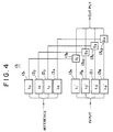
- FIG.4 shows the construction of the filter 13 used in the system of FIG.3.
- the filter 13 includes a number of filter elements 13 1 - 13 4 respectively passing the optical beams of the wavelengths ⁇ a - ⁇ d , as well as a number of filter elements 13 5 - 13 8 respectively passing the optical beams of the wavelengths ⁇ 1 ' - ⁇ 4 ', wherein the wavelength-multiplexed input optical beam is supplied to each of the filter elements 13 5 - 13 8 parallel with each other. Further, the reference optical beam is supplied parallel to each of the filter elements 13 1 - 13 4 .
- the output optical beams of the filter elements 13 5 - 13 8 are supplied to corresponding variable transmittance controllers 13 9 - 13 12 each having a transmittance that is controlled in response to the output of the corresponding filter element.
- the transmittance of the controller 13 9 is selectively increased and the optical signal having the wavelength ⁇ 1 ' and passed through the filter element 13 5 is selectively outputted as an output optical beam of the filter 13.
- This, of course, is not the essential requirement for the operation of the device.
- FIG.5 shows an example of the variable transmittance controllers 13 9 - 13 12 , wherein the input optical signal from the filter 13 5 - 13 9 is supplied to a laser amplifier 13 23 for amplification by the stimulated emission caused therein in response to the passage of the wavefront of the input optical beam.
- the operation of the laser amplifier 13 23 is controlled by an electronic control circuit 13 22 that in turn is controlled in response to an electric signal produced by a photodetector 13 21 to which the reference optical beam is supplied.
- the electronic circuit 13 22 produces a bias signal to the laser amplifier 13 23 when there is an incident reference optical beam to the photodetector 13 21 .
- the laser amplifier 13 22 amplifies the incident input optical signal, while when there is no bias signal, the laser amplifier 13 22 absorbs the input optical signal.
- a Franz-Keldysh effect device or MQW optical modulator that uses the quantum confinement Stark effect.
- FIG.6 shows another embodiment of the variable-wavelength filter 13 wherein there is provided an optical switch 13 31 that has a first input port B for receiving the reference optical beam and a second input port A for receiving the input optical beam, wherein one of the optical beams at the input port A and the input port B is supplied selectively to a filter device 13 32 of which wavelength is controlled by a controller 13 34 .
- the optical beam that has passed through the filter device 13 32 is supplied to a second optical switch 13 33 that has a first output port C connected to an output waveguide (not shown) and a second output port D connected to the controller 13 34 .
- the first optical switch 13 31 is set at first such that the input port B is selected. Further, the second optical switch 13 33 is set such that the output port D is selected.
- the reference optical beam supplied to the input port B is transferred to the controller 13 34 after passing through the filter device 13 32 and the switch 13 33 .
- the controller 13 34 sets the state of the filter device 13 32 such that the transmittance of the optical beam becomes maximum.
- the state of the optical switches 13 31 and 13 33 switched such that the input optical beam at the port A is outputted at the port C after passing through the filter device 13 32 .
- the system 13 acts as the variable-wavelength filter that passes the optical signal having a wavelength coincident to the wavelength of the reference optical beam selectively.
- FIG.7 shows the construction of the filter device 13 32 .
- the filter device 13 32 is formed of a DFB laser diode that has an active layer 13 41 and a diffraction grating 13 42 .
- the device is biased below the threshold of laser oscillation. Thereby, the incident optical beam causes a stimulated emission in the active layer 13 41 upon passage therethrough.
- FIG.8 shows the band-pass characteristics of the laser amplifier of FIG.7 for different bias voltages. As can be seen in FIG.8, the peak of the transmittance shifts in response to the bias voltage. By using this effect, one can set the pass-band or pass-wavelength in the filter device by means of the controller 13 43 .
- the optical switches 13 31 and 13 33 one may use the directional coupler and saturable optical absorption switch that changes the transmittance in response to the injection of carriers.
- FIG.9 shows a wavelength-synchronized optical processing device according to a second embodiment of the present invention.
- the device includes an optical processing unit 11a and a control unit 11b, wherein the optical processing unit 11a uses the photodetector 14 for detecting the input optical beam that has the wavelength of ⁇ i ' similarly to the optical processing unit 11 of the first embodiment.
- This input optical beam may have the fluctuation in the wavelength ⁇ i '.
- the output electric signal of the photodetector 14 is supplied to the optical modulator 15 that in turn is supplied with the reference optical beam of the wavelength ⁇ i .
- the optical modulator 15 modulates the reference optical beam with the output electric signal of the photodetector 14, and an output optical beam carrying the optical signal of the original wavelength ⁇ i ' is obtained with a stabilized wavelength of ⁇ i .
- a control unit 12a is used for controlling the operation of the optical modulator 15.
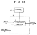
- FIG.10 shows a wavelength-synchronized optical processing device according to a third embodiment of the present invention.
- the optical processing device is formed of an optical processing unit 11b and a control unit 12b, wherein there is provided a laser diode 16 that is controlled by a controller 12b.
- the laser diode is injected with the reference optical beam of the stabilized wavelength ⁇ i and further with the input optical beam of the wavelength ⁇ i ' for producing an output optical beam carrying thereon the information modulated on the input optical beam, with the wavelength of ⁇ i .
- the laser diode acts as the wavelength converter.
- the optical signal of the wavelength ⁇ i ' and containing fluctuation is converted to the optical signal of the wavelength ⁇ i that is free from fluctuation.
- FIG.11 shows a fourth embodiment of the optical processing device according to the present invention.
- the optical processing device of the present embodiment has a construction similar to that of FIG.3 except that there is provided a wavelength converter 17 after the optical processing unit 11 for converting the wavelength of the output optical beam from the wavelength ⁇ i to another wavelength ⁇ k .
- a wavelength converter 17 After the optical processing unit 11 for converting the wavelength of the output optical beam from the wavelength ⁇ i to another wavelength ⁇ k .
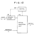
- FIG.12 shows the optical processing device according to a fifth embodiment of the present invention.
- the optical processing device of the present embodiment has a structure similar to that of FIG.10 except that there is provided a variable-wavelength filter 18 provided for filtering the input optical beam.
- the variable-wavelength filter 18 is controlled by the controller 12b and selectively passes one of the optical signals multiplexed on the input optical beam with the wavelengths ⁇ 1 ' - ⁇ n '. In this case, too, any of the desired optical signals that are multiplexed on the input optical beam with the wavelength-multiplex mode is converted to the desired, stabilized wavelength ⁇ i .
- FIG.13 shows an optical path selector according to a sixth embodiment of the present invention, wherein a number of optical processing devices 21 1 - 21 n are used.
- the optical path selector of the present embodiment uses a number of electro-optic converters 23 1 - 23 n , wherein each electro-optic converter may be formed from a laser diode that produces an optical signal with a wavelength that is pertinent to the laser diode.
- the electro-optic converter 23 1 produces the optical signal with a wavelength ⁇ 1
- the electro-optic converter 23 2 produces the optical signal with a wavelength ⁇ 2
- the electro-optic converter 23 n produces the optical signal with a wavelength ⁇ n .
- the output optical signals of these electro-optic converters are supplied to an optical synthesis and distribution unit 24 that synthesizes a wavelength-multiplex optical signal from these optical signals.
- each optical processing device 21 1 - 21 n has a construction similar to any of the wavelength-synchronized optical processing devices described previously.
- a reference optical beam generator 22 that includes a number of stabilized laser diodes each stabilized in terms of the temperature and bias current and produces the reference optical beam with stabilized wavelengths.
- the reference optical beam thus produced is supplied to the optical processing devices 21 1 - 21 n as the reference optical beam as described previously, and each optical processing device produces an output optical beam with the stabilized wavelength that is specified by the wavelength of the reference optical beam.
- the original optical signal having the wavelength ⁇ 1 is selectively outputted to the optical transmission line connected to the optical processing device 21 1 with the stabilized wavelength of ⁇ 1 .
- the optical processing device 21 1 may be supplied with the optical output signal of the wavelength ⁇ 2 from the electro-optic converter 23 2 and output the same on the transmission line connected to the device 21 1 with the wavelength of ⁇ 1 .
- the selection of the wavelength of the input optical signal at the optical processing device 21 1 - 21 n may be achieved by the control unit provided in each of the optical processing device.
- the system of the present embodiment is suited for use in optical path selectors or optical transmitters that send the wavelength-multiplex optical signals with stabilized wavelengths.
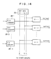
- FIG.14 shows the block diagram of an optical transmitter according to a seventh embodiment of the present invention.
- the electro-optic converters wherein the electro-optic converters are grouped into a number of groups each including the electro-optic converters 23 1 - 23 n .
- the output optical beams produced by these electro-optic converters are supplied to corresponding optical processing devices 21 1 - 21 n directly similar to the embodiment of FIG.14.
- the reference optical beam generator 22 produces the reference optical beams with the wavelengths of ⁇ 1 , ⁇ 2 , . . ., ⁇ n similar to the embodiment of FIG.13. Thereby, the wavelengths ⁇ 1 - ⁇ n are changed from each other in each group while the reference optical beams are supplied to the optical processing devices of other groups in parallel.
- the optical processing device can produce the optical signals with any desired wavelengths by supplying thereto suitable reference optical beams from the generator 22.
- suitable reference optical beams For example, one can obtain the output optical signal from the device 21 1 by supplying the reference optical beam thereto with the wavelength of ⁇ n .
- the present embodiment is useful for the optical transmitters and the optical repeaters.
- the system of FIG.14 can be configured to form a number of optical channels each carrying the wavelength-multiplexed optical signals of the wavelengths of ⁇ 1 - ⁇ n .
- FIG.15 shows an optical matrix switch according to an eighth embodiment of the present invention, wherein there are provided a number of optical transmission lines 33 at the input side and a number of optical transmission lines 34 at the output side.
- wavelength-multiplexed optical signals are supplied with wavelengths ⁇ 1 ' - ⁇ n ', while on each transmission line 34 of the output side, wavelength-multiplexed optical signals are carried with wavelengths of ⁇ 1 - ⁇ n .
- a wavelength-synchronized optical processing device 31 that has a construction of any of the foregoing embodiments of FIGS.3 - 12, and each optical processing system 31 is supplied with the reference optical beam that is produced by a reference optical beam generator 32 with the stabilized wavelengths of ⁇ 1 - ⁇ n .
- the optical processing device 31 causes a transfer of the input optical signal of the selected wavelength from the transmission line 33 of the input side to the optical transmission line 34 of the output side, wherein the optical signal thus transferred has a stabilized wavelength that is specified by the wavelength of the reference optical beam.
- each optical transmission line 34 carries thereon a number of wavelength multiplexed optical signals produced by a group of the optical processing devices 31 that are connected commonly to a single optical transmission line 33.
- the group of the optical processing devices 31 that are provided commonly on one optical transmission line 33 are supplied with a single reference optical beam commonly, and the wavelength of the reference optical beam is changed in each optical transmission line 33.
- optical signals of different wavelengths are outputted on each optical transmission line 34 of the output side.
- FIG.16 shows the details of the optical matrix switch of FIG.15.
- an optical divider 35 on the optical transmission line in correspondence to each of the optical processing devices 31 for tapping the wavelength-multiplexed optical signals on the transmission line 33, and the optical signals thus tapped are supplied to the optical processing device 31.
- the optical processing device 31 selects one of the optical signals on the line 33 and outputs the selected optical signal with the wavelength of the reference optical beam.
- the output optical beam of the optical processing device 31 in turn is supplied to an optical coupler 36 that is provided on the optical transmission line 34 in correspondence to each of the optical processing device 31.
- the optical coupler 36 establishes an optical coupling between an optical fiber or waveguide that carries the optical output of the system 31 and the optical fiber or waveguide forming the optical transmission line 34, and the optical beam outputted from the optical processing device 31 is merged or wavelength-multiplexed upon the optical signals on the line 34.
- an optical matrix switch can be constructed in the form of optical integrated circuit by forming the optical divider 35 and the optical coupler 36 together with the optical processing device 31 and the reference optical beam generator 32 on a common substrate.
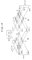
- FIG.17 shows an optical matrix switch according to a ninth embodiment of the present invention.
- two optical matrix switches 38 and 39 each having the construction of FIG.16 are connected in series, wherein the matrix switches 38 and the matrix switches 39 are connected by intermediate optical transmission lines 37 1 - 37 n .
- These optical transmission lines act as the optical transmission lines at the output side for the optical matrix switch 38 while act simultaneously as the input side optical transmission lines for the optical matrix switch 39.
- the reference optical beam generator 32 is used commonly for both the optical matrix switch 38 and the optical matrix switch 39, wherein the reference optical beam generator 32 supplies the reference optical beams to the optical matrix 38 and the optical matrix 39 independently.
- the reference optical beam having the wavelength of ⁇ 1 is supplied to a group of the optical processing devices 31 that are located at the intersections formed between the line 33 1 and the lines 37 1 - 37 n
- the reference optical beam having the wavelength of ⁇ 2 is supplied to another group of the optical processing devices 31 that are located at the intersections formed between the line 33 2 and the lines 37 1 - 37 n
- the wavelength of the reference optical beam supplied to a group of the optical processing devices 31 that are provided on a common optical transmission line of the input side is changed with respect to the wavelength of the reference optical beam that is supplied to the to another group of the optical processing devices 31 that are provided commonly on another input side optical transmission line.
- optical signals thus outputted on the lines 37 1 - 37 n are then switched by the second optical matrix switch 39, wherein the optical switching similar to the one described with reference to the optical matrix switch 38 is achieved.
- output optical signals having respective wavelengths determined by the wavelength of the reference optical beams supplied to the optical matrix switch 39 are obtained at the output optical transmission lines 34 1 - 34 n .
- the wavelength of these output optical signals is of course stabilized by using the stabilized optical source for the reference optical beam generator 32.
- FIG.18 shows a tenth embodiment of the present invention, wherein the present embodiment forms a wavelength converter for converting the wavelength of the optical signals modulated on the input optical beam with the wavelength-multiplex mode and outputting the optical signals thus converted in the wavelength multiplex mode.
- each of the optical processing devices 41 1 - 41 n is supplied with the wavelength-multiplex optical signals from the optical distribution part 44 that in turn is supplied with an input optical beam carrying the wavelength-multiplex signals and distributing the same to the optical processing devices 41 1 - 41 n .
- the optical processing devices 41 1 - 41 n are controlled by a control unit 43 that selects an optical signal from the wavelength-multiplexed optical signals.
- the control unit 43 controls a variable-wavelength filter similar to the filter 13 of FIG.3. Thereby, the control unit 43 acts as the control unit 12.
- a reference optical beam generator 42 that produces the reference optical beam with the wavelengths ⁇ 1 , ⁇ 2 , . . ., ⁇ n and supply the same to respective optical processing devices.
- the optical processing devices 41 1 - 41 n produce output optical beams in coincidence with respective wavelengths of the reference optical beams.
- the output optical beams thus produced are added in an optical synthesis unit 45 that produces the an output optical beam on which the optical signals are modulated in the wavelength-multiplex mode.
- FIG.19 shows an eleventh embodiment of the present invention.
- the optical processing system of the present embodiment includes a number of wavelength-synchronized optical processing devices 51 11 - 51 mn described previously with reference to FIGS.3 - 12 and a reference optical beam generator 52 for producing the reference optical beam.
- each transmission line is connected to a corresponding optical distribution unit 55 1 - 55 m and supplies thereto a wavelength-multiplexed input optical beam.
- the input optical beam carries thereon the optical signals of the wavelengths ⁇ 1 ' - ⁇ n '.
- Each optical distribution unit such as the unit 55 1 is connected to a number of optical processing devices such as 51 11 - 51 1n for supplying the wavelength-multiplexed optical signals to each of these devices.
- the optical processing devices are supplied with the reference optical beams from the reference optical beam generator 52 with selected wavelengths and produce the output optical signals with the wavelength specified by the wavelength of the reference beams.
- the reference optical beam of the wavelength ⁇ 1 is supplied to the optical processing devices 51 11 - 51 1n commonly, the reference optical beam of the wavelength ⁇ 2 is supplied to the optical processing devices 51 21 - 51 2n (not shown) commonly, . . . and the reference optical beam of the wavelength ⁇ n is supplied to the optical processing devices 51 m1 - 51 mn , commonly.
- the reference optical signals produced from the optical processing devices 51 11 - 51 1n have the wavelength ⁇ 1
- all the output optical signals produced from the optical processing devices 51 21 - 51 2n have the wavelength ⁇ 2 , ⁇ ⁇ ⁇
- all the output optical signals from the optical processing devices 51 m1 - 51 mn have the wavelength of ⁇ n .
- the optical output of each optical processing device is supplied to a corresponding optical synthesis unit such that each optical synthesis unit is supplied with optical signals of mutually different wavelengths from different optical processing devices.
- the output optical signal of the optical processing device 51 11 is supplied to an optical synthesis unit 56 1
- the optical output of the optical processing device 51 12 is supplied to an optical synthesis unit 56 2 (not shown) . . .
- the optical output of the optical processing device 51 1n is supplied to an optical synthesis unit 56 m . It should be noted that all the optical output signals mentioned above have the wavelength of ⁇ 1 .
- the optical synthesis unit 56 1 When viewed from the side of the optical synthesis unit, the optical synthesis unit 56 1 is supplied with the output optical signals from the optical processing devices 51 11 , 51 21 , . . . 51 m1 with the wavelengths of ⁇ 1 , ⁇ 2 , . . . ⁇ n and produces an output optical beam on which these optical signals are multiplexed in the wavelength-multiplex mode.
- the optical synthesis unit 56 m is supplied with the output optical signals from the optical processing devices 51 1n , 51 2n , . . . 51 mn with respective wavelengths of ⁇ 1 , ⁇ 2 , . . . ⁇ n and produces an output optical beam on which the optical signals are multiplexes in the wavelength-multiplex mode.
- the system of FIG.19 converts the wavelength of the optical signals from ⁇ 1 ' - ⁇ n ' to ⁇ 1 - ⁇ n and simultaneously stabilizes the wavelength of the output optical signals. It should be noted that any combination of the optical signals supplied on the input side optical transmission lines 53 1 - 53 m can be obtained on each of the output side transmission lines 54 1 - 54 m in the form of wavelength-multiplexed optical signals.
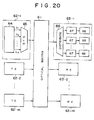
- FIG.20 is a block diagram showing the construction of an optical information transmission system wherein an optical matrix switch 61 having the construction of FIG.15 or FIG.17 is used.
- optical transmission terminals 62 1 - 62 m connected to the input side optical transmission lines of the optical matrix switch 61. Further, a number of optical reception terminals 63 1 - 63 m are connected to the output side optical transmission lines of the matrix switch 61.
- Each optical transmission terminal such as the terminal 62 1 includes an optical transmitter 64 for producing a number of optical signals with respective wavelengths ⁇ 1 - ⁇ n and an optical synthesizing unit 65 supplied with the optical signals for producing a wavelength-multiplexed optical beam from the optical signals.
- each optical reception terminal such as the terminal 63 1 includes an optical distribution unit 66 supplied with the wavelength-multiplexed optical signals from the optical matrix switch 61 and a variable-wavelength filter 67 for selecting an optical signal of a specific wavelength.
- a photodetector 68 in connection with the filter 67 for detecting the optical signal that has passed through the filter 67.
- the optical matrix switch 61 By controlling the optical matrix switch 61 in accordance with control information such as the address information, the path and the wavelength of the optical signals are switched in the matrix switch 61. More specifically, one can switch a huge number of channels (number of wavelength multiplex signals X number of transmission lines) simultaneously by using the system of FIG.20.
- FIG.21 shows a thirteenth embodiment of the present invention.
- the system of the present embodiment is also an optical transmission system, wherein there are provided a number of transmission terminals 73 1 - 73 m each supplied with electric signals and producing optical signals in correspondence to the electric signals with respective wavelengths.
- the output optical signals of the terminals 73 1 - 73 m are supplied to an optical path selector 71 that includes a number of optical synthesis and distribution units 75 as well as 76 provided in correspondence to the transmission terminals 73 1 - 73 m and the reception terminals 74 1 - 74 m .
- the optical path selector 71 has a construction similar to the system shown in FIG.19, and the output optical signals of each transmission terminal are mixed to form a wavelength-multiplexed optical signal similar to the embodiment of FIG.19.
- wavelength-multiplexed optical signals are selected by the optical processing devices similar to the devices of 51 11 - 51 mn and are distributed further to a number of optical synthesis and distribution units 76 provided in correspondence to the optical reception terminals 74 1 - 74 m .
- the optical processing devices are not illustrated for the sake of clarity of the drawing. There, any combination of the optical signals produced by the optical transmission terminals 73 1 - 73 m is obtained at the output of each optical synthesis and distribution unit 76 in the form of the wavelength-multiplexed optical signals.
- the optical output thus obtained is then selectively passes through a filter 77 and detected by a photodetector 78.
- a photodetector 78 In this case, too, one can switch a large number of connections of which number is given by the product of the number of wavelength-multiplex signals and the number of optical transmission lines or channels, simultaneously.
Landscapes
- Engineering & Computer Science (AREA)
- Computer Networks & Wireless Communication (AREA)
- Physics & Mathematics (AREA)
- Electromagnetism (AREA)
- Signal Processing (AREA)
- Optical Communication System (AREA)
- Use Of Switch Circuits For Exchanges And Methods Of Control Of Multiplex Exchanges (AREA)
- Lasers (AREA)
Abstract
Description
- The present invention generally relates to optical processing systems and more particularly to a wavelength-synchronized optical processing device that produces an optical signal with a wavelength that is synchronized to a stabilized wavelength of a reference optical beam and various optical information processing systems that use such an optical processing device.
- With the extensive deployment of optical telecommunication network, studies are made on the optical transmission and reception in the optical exchange systems and optical subscriber systems. Among others, there is a proposal to transmit a plurality of optical signals having different wavelengths on a common optical fiber or optical waveguide in the wavelength multiplex mode. In such a wavelength multiplex transmission of optical signals, it is necessary to superpose the optical signals with sufficient wavelength interval such that a reception side can demultiplex the received optical signal into individual optical signal components with reliability. In such wavelength multiplex systems, it will be easily understood that the change or fluctuation of the oscillation wavelength occurring in the optical signals cause a disastrous effect in the operation of the reception side systems.
- FIG.1 shows the block diagram of a conventional optical processing system that uses a wavelength converter 1a.
- Referring to FIG.1, the wavelength converter 1a is supplied with an input optical signal having a wavelength of λ0 and produces an output optical signal with a wavelength of λ1. There, the wavelength converter converts the wavelength of the input optical signal to a second wavelength, and the optical signal having the wavelength λ1 is divided out from the converted optical signal in response to a reference optical beam given externally with the wavelength λ1.
- More specifically, the output optical signal of the wavelength converter 1a is supplied to an
optical divider 2a that divides the incident optical beam into a first output beam corresponding to the output optical signal and a second output beam, and the second output beam is supplied to a wavelength comparator 3a. The wavelength comparator 3a is further supplied with the reference optical beam and produces an electric output indicative of the difference between the wavelength of the output optical signal of the converter 1a and the wavelength λ1 of the reference optical beam. - The output electric signal of the comparator 3a is supplied to a controller 4a that in turn produces a control signal for controlling the operation of the wavelength converter 1a. According to this system, one can convert the wavelength λ0 of the incident optical signal to the wavelength λ1 by controlling the converter 1a such that the output of the wavelength comparator 3a becomes zero. The wavelength converter 1a may be formed by using a DFB laser diode that can change the oscillation wavelength by controlling the bias current or temperature.
- FIG.2 shows another conventional wavelength conversion system wherein an input optical signal having a wavelength λ0 is supplied to a photoelectric converter 1b that produces an electric output in response to the incident optical signal. The output electric signal is supplied to a
clock extraction circuit 2b wherein a clock signal is extracted from the information that is modulated on the input optical signal. The clock extraction circuit further discriminates the logic level of the binary information signal modulated on the input optical beam with a timing given by the clocks, and drives anoptical modulator 3b. Theoptical modulator 3b is thereby supplied with a reference optical beam with the wavelength λ1 and modulates the same in accordance with the electric output of theclock extraction circuit 2b. As a result, an optical output signal is obtained with the wavelength λ1. - In any of these conventional optical processing systems, there has been a problem in that the normal operation of the system is not achieved when there is a fluctuation in the wavelength of the input optical beam. It should be noted that, in the telecommunication systems, there is no guarantee that the transmission side uses the stabilized optical source with respect to the oscillation wavelength. Further, such a fluctuation of the wavelength of the optical signal may be caused as a result of the dispersion of optical pulses that occur in the optical fibers. Thus, the optical transmission system is not only required to eliminate the fluctuation of the wavelength of the optical source at the transmission side but is also required to have an ability to adapt to the fluctuation of wavelength and to eliminate the same at the reception side or at any intermediate locations between the transmission side and the reception side.
- Accordingly, it is a general object of the present invention to provide a novel and useful wavelength-synchronized optical processing device, wherein the foregoing problems are eliminated.
- Another and more specific object of the present invention is to provide a wavelength-synchronized optical processing device for use in an optical transmission system wherein the optical processing device is capable of eliminating the fluctuation of wavelength from an optical beam that is transmitted through the optical transmission system.
- Another object of the present invention is to provide a wavelength-synchronized optical processing device comprising an optical processing unit supplied with an input optical beam carrying thereon one or more optical signals having respective, mutually different wavelengths, for producing an output optical signal with a wavelength specified by the wavelength of a reference optical beam that is supplied to the optical processing unit externally, and a controller for controlling the operation of the optical processing unit. According to the present invention, one can select any optical signal component of the desired wavelength from the optical signals modulated on the input optical beam with the wavelength-multiplexed mode. Thereby, the wavelength of the input optical signal is synchronized to the stabilized wavelength of the reference optical beam and one can obtain the output optical signals with the accurate wavelength even when there is a substantial fluctuation in the wavelength of the incident optical signals.
- In a preferred embodiment, the optical processing unit comprises a variable wavelength filter supplied with the input optical signal and controlled by the controller for selectively passing the optical signal having the wavelength specified by the wavelength of the reference optical beam, a photoelectric converter supplied with an optical output of the variable wavelength filter for converting the same to an electric signal, and an optical modulator supplied with the output electric signal of the photoelectric converter for modulating an optical beam having the wavelength of the reference optical beam in response to the electric signal. According to the present invention, one can extract a desired optical beam having a wavelength that is synchronized to the reference wavelength from the wavelength-multiplexed input optical beam. The optical processing unit may further include a wavelength converter for converting the wavelength of the output optical beam to a desired wavelength. Thereby, one can reestablish the wavelength multiplex of the optical signals with the interval of the wavelength set stably.
- Another object of the present invention is to provide an optical switching system comprising an electro-optic converter supplied with input electric signals of different channels for producing optical signals in correspondence to the input electric signals with respective, mutually different wavelengths, an optical distribution unit supplied with the output optical signals from the electro-optic converter for merging and distributing the optical signals into a plurality of physically separated optical channels, and a wavelength-synchronized optical processing device provided on each of the optical channels for producing a stabilized optical output that has a wavelength stabilized with respect to an wavelength of a reference optical beam, and a reference beam generator for producing the reference optical beam with a stabilized wavelength. According to the present invention, one can direct the information signal to any optical channels by merging the optical signals at the optical distribution unit and recovering the original information therefrom at the wavelength-synchronized optical processing device by selecting the wavelength of the reference optical beam produced by the reference beam generator. Thereby, the exchange of signals between a huge number of channels is achieved with a simple construction of the switching system.
- In a preferred embodiment of the present invention, the optical channels are grouped into a plurality of channel groups each including a plurality of channels, and the reference beam generator supplies the reference optical beam to the plurality of channel groups commonly such that the wavelength of the reference beam is changed in each channel in one channel group.
- Another object of the present invention is to provide an optical switching system comprising a plurality of input-side optical channels for guiding wavelength-multiplexed optical signals therethrough, a plurality of output-side channels for guiding output optical signals therethrough, each of said input-side optical channels and each of said output-side optical channels being crossed with each other at a node, wherein there is provided a wavelength-synchronized optical processing device in correspondence to each node, said optical processing device comprising: an optical processing unit supplied with said wavelength-multiplexed input optical signal and a reference optical beam having a reference wavelength for transferring selectively an optical signal that has a wavelength specified by the reference wavelength from the optical input channel to the optical output channel; and a reference beam generator for producing the reference optical beam with said reference wavelength. According to the present invention, the transfer of optical signals from the plurality of input-side optical channels to a desired output-side optical channel is achieved while simultaneously stabilizing the wavelength of the output optical beam on the output-side optical channel. Further, a number of optical output signals having different wavelengths are multiplexed on the output-side optical channel at the plurality of nodes and one obtains a wavelength-multiplexed optical signal with stabilized wavelengths.
- In a preferred embodiment, one may provide intermediate optical channels to link the input-side optical channels and the output-side optical channels, with the optical processing unit and the reference beam generator provided at each node between the input-side optical channels and the intermediate optical channels and further at each node between the intermediate optical channels and the output-side optical channels.
- Another object of the present invention is to provide a variable-wavelength filter device that is supplied with a control signal having a controlled wavelength for selectively transmitting an incident optical beam that has a wavelength specified by the controlled wavelength.
- Other objects and further features of the present invention will become apparent from the following detailed description when read in conjunction with the attached drawings.
-
- FIG.1 is a block diagram showing the construction of a conventional wavelength conversion circuit used in an optical transmission system;
- FIG.2 is a block diagram showing another conventional wavelength conversion circuit;
- FIG.3 is a block diagram showing the construction of the wavelength-synchronized optical processing device according to a first embodiment of the present invention;
- FIG.4 is a block diagram showing the construction of a variable filter used in the optical processing device of FIG.3;
- FIG.5 is a block diagram showing another example of the variable filter of FIG.4;
- FIG.6 is a block diagram showing still another construction of the variable filter of FIG.4;
- FIG.7 is a diagram showing the structure of a semiconductor optical device used in the variable filter of FIG.6;
- FIG.8 is a diagram showing the operational characteristics of the device of FIG.7;
- FIG.9 is a block diagram showing the construction of the wavelength-synchronized optical processing device according to a second embodiment of the present invention;
- FIG.10 is a block diagram showing the construction of the wavelength-synchronized optical processing device according to a third embodiment of the present invention;
- FIG.11 is a block diagram showing the construction of the wavelength-synchronized optical processing device according to a fourth embodiment of the present invention;
- FIG.12 is a block diagram showing the construction of the wavelength-synchronized optical processing device according to a fifth embodiment of the present invention;
- FIG.13 is a block diagram showing the construction of the optical transmitter according to a sixth embodiment of the present invention that uses the wavelength-synchronized optical processing device;
- FIG.14 is a block diagram showing the construction of the optical transmitter according to a seventh embodiment of the present invention that uses the wavelength-synchronized optical processing device;
- FIG.15 is a block diagram showing the construction of an optical matrix switch according to an eighth embodiment of the present invention that uses the wavelength-synchronized optical processing device;
- FIG.16 is a block diagram showing the essential part of the optical matrix switch of FIG.15;
- FIG.17 is a block diagram showing the construction of an optical matrix switch according to a ninth embodiment of the present invention;
- FIG.18 is a block diagram showing the construction of the optical switching system according to a tenth embodiment of the present invention wherein the wavelength-synchronized optical processing device is used;
- FIG.19 is a block diagram showing the construction of the optical switching system according to an eleventh embodiment of the present invention;
- FIG.20 is a block diagram showing the construction of the optical transmission system according to a twelfth embodiment of the present invention; and
- FIG.21 is a block diagram showing the construction of the optical transmission system according to a thirteenth embodiment of the present invention wherein the wavelength-synchronized optical processing device is used.
-
- FIG.3 shows the general construction of the wavelength-synchronized optical processing device according to a first embodiment of the present invention. The optical processing device of FIG.3 is an optical demultiplexer that selectively recovers an optical signal component from a wavelength-multiplex optical signal modulated on an input optical beam, in response to a reference optical beam that specifies the wavelength of the optical signal to be recovered.
- Referring to FIG.3, the optical processing device includes an optical processing unit 11 and a
control unit 12, wherein the optical processing unit 11 is generally formed from a variable-wavelengthband pass filter 13, aphotodetector 14 and anoptical modulation unit 15. Theband pass filter 13 of the optical processing unit 11 is supplied with an incident optical beam and controlled by thecontrol unit 12 such that only the optical signal that has a particular wavelength specified by thecontrol unit 12 is passed through thefilter 13. - The output optical beam of the
filter 13 is supplied to thephotodetector 14 wherein thephotodetector 14 converts the optical beam to an electric signal. The output electric signal of thephotodetector 14 is supplied to theoptical modulation unit 15 and theoptical modulation unit 15 modulates the reference optical beam in response to the electric output of thephotodetector 14. As will be described later in detail, thefilter 13 may be formed of a DFB laser amplifier and changes the wavelength of the optical beam passing therethrough in response to a bias current that is controlled below the threshold of laser oscillation. Theoptical modulation unit 15 may be a Franz-Keldysh effect device or a laser diode of which gain can be changed in response to the output of thephotodetector 14. - In operation, an input optical beam that carries thereon optical signals having respective wavelengths λ1' - λn' in the wavelength-multiplex mode is supplied to the
filter 13 that in turn is controlled by thecontrol unit 12 to pass the optical signal having the wavelength λi' selectively. Meanwhile, the wavelength of the reference beam is well stabilized by using a stabilized optical source such as a laser diode of which operational temperature and bias current are compensated for with respect to any variation. Thereby, one obtains the output optical signal from theoptical modulation unit 15 with the wavelength λi in correspondence to foregoing original optical signal of the wavelength λi'. The circuit 11 can be formed as an integrated circuit including thecontrol unit 12. - FIG.4 shows the construction of the
filter 13 used in the system of FIG.3. - Referring to FIG.4, the
filter 13 includes a number of filter elements 131 - 134 respectively passing the optical beams of the wavelengths λa - λd, as well as a number of filter elements 135 - 138 respectively passing the optical beams of the wavelengths λ1' - λ4', wherein the wavelength-multiplexed input optical beam is supplied to each of the filter elements 135 - 138 parallel with each other. Further, the reference optical beam is supplied parallel to each of the filter elements 131 - 134. - The output optical beams of the filter elements 135 - 138 are supplied to corresponding variable transmittance controllers 139 - 1312 each having a transmittance that is controlled in response to the output of the corresponding filter element. Thus, when the reference optical beam is given with the wavelength of λa, the transmittance of the
controller 139 is selectively increased and the optical signal having the wavelength λ1' and passed through thefilter element 135 is selectively outputted as an output optical beam of thefilter 13. - In the present embodiment, one may employ any of the multi-layered dielectric films, optical waveguides, or the spatial filters that use the diffraction grating, for the filter element 135 - 139. Preferably, the wavelengths λa, λb' λc and λd may be set coincident to the wavelengths λ1', λ2', λ3' and λ4' such that λa = λ1', λb = λ2', λc = λ3' and λd = λ4'. This, of course, is not the essential requirement for the operation of the device.
- FIG.5 shows an example of the variable transmittance controllers 139 - 1312, wherein the input optical signal from the filter 135 - 139 is supplied to a
laser amplifier 1323 for amplification by the stimulated emission caused therein in response to the passage of the wavefront of the input optical beam. The operation of thelaser amplifier 1323 is controlled by anelectronic control circuit 1322 that in turn is controlled in response to an electric signal produced by aphotodetector 1321 to which the reference optical beam is supplied. - More specifically, the
electronic circuit 1322 produces a bias signal to thelaser amplifier 1323 when there is an incident reference optical beam to thephotodetector 1321. In response to the bias signal, thelaser amplifier 1322 amplifies the incident input optical signal, while when there is no bias signal, thelaser amplifier 1322 absorbs the input optical signal. For the variable transmittance controllers, one may use, in addition to the foregoing laser amplifier, a Franz-Keldysh effect device or MQW optical modulator that uses the quantum confinement Stark effect. - FIG.6 shows another embodiment of the variable-
wavelength filter 13 wherein there is provided anoptical switch 1331 that has a first input port B for receiving the reference optical beam and a second input port A for receiving the input optical beam, wherein one of the optical beams at the input port A and the input port B is supplied selectively to afilter device 1332 of which wavelength is controlled by acontroller 1334. The optical beam that has passed through thefilter device 1332 is supplied to a secondoptical switch 1333 that has a first output port C connected to an output waveguide (not shown) and a second output port D connected to thecontroller 1334. - In operation, the first
optical switch 1331 is set at first such that the input port B is selected. Further, the secondoptical switch 1333 is set such that the output port D is selected. In this state, the reference optical beam supplied to the input port B is transferred to thecontroller 1334 after passing through thefilter device 1332 and theswitch 1333. Thereby, thecontroller 1334 sets the state of thefilter device 1332 such that the transmittance of the optical beam becomes maximum. After such a training of thefilter device 1332 is completed, the state of theoptical switches filter device 1332. Thereby, only the optical signal that has the wavelength coincident to the wavelength of thefilter device 1332 alone appears at the output port C. In other words, thesystem 13 acts as the variable-wavelength filter that passes the optical signal having a wavelength coincident to the wavelength of the reference optical beam selectively. - FIG.7 shows the construction of the
filter device 1332. - Referring to FIG.7, the
filter device 1332 is formed of a DFB laser diode that has anactive layer 1341 and adiffraction grating 1342. In operation, the device is biased below the threshold of laser oscillation. Thereby, the incident optical beam causes a stimulated emission in theactive layer 1341 upon passage therethrough. - FIG.8 shows the band-pass characteristics of the laser amplifier of FIG.7 for different bias voltages. As can be seen in FIG.8, the peak of the transmittance shifts in response to the bias voltage. By using this effect, one can set the pass-band or pass-wavelength in the filter device by means of the
controller 1343. - According to the construction of FIG.6, one can maintain the stable operational characteristics for the
filter 13 as a whole even when there is a change in the operational characteristics of the laser amplifier itself. Obviously, this is due to the feedback control of thelaser amplifier 1332 as described above. For theoptical switches - FIG.9 shows a wavelength-synchronized optical processing device according to a second embodiment of the present invention.
- Referring to FIG.9, the device includes an optical processing unit 11a and a control unit 11b, wherein the optical processing unit 11a uses the
photodetector 14 for detecting the input optical beam that has the wavelength of λi' similarly to the optical processing unit 11 of the first embodiment. This input optical beam may have the fluctuation in the wavelength λi'. - The output electric signal of the
photodetector 14 is supplied to theoptical modulator 15 that in turn is supplied with the reference optical beam of the wavelength λi. Thereby, theoptical modulator 15 modulates the reference optical beam with the output electric signal of thephotodetector 14, and an output optical beam carrying the optical signal of the original wavelength λi' is obtained with a stabilized wavelength of λi. Further, a control unit 12a is used for controlling the operation of theoptical modulator 15. - FIG.10 shows a wavelength-synchronized optical processing device according to a third embodiment of the present invention.
- Referring to FIG.10, the optical processing device is formed of an optical processing unit 11b and a
control unit 12b, wherein there is provided alaser diode 16 that is controlled by acontroller 12b. There, the laser diode is injected with the reference optical beam of the stabilized wavelength λi and further with the input optical beam of the wavelength λi' for producing an output optical beam carrying thereon the information modulated on the input optical beam, with the wavelength of λi. Thereby, the laser diode acts as the wavelength converter. Again, the optical signal of the wavelength λi' and containing fluctuation is converted to the optical signal of the wavelength λi that is free from fluctuation. - FIG.11 shows a fourth embodiment of the optical processing device according to the present invention.
- Referring to FIG.11, the optical processing device of the present embodiment has a construction similar to that of FIG.3 except that there is provided a
wavelength converter 17 after the optical processing unit 11 for converting the wavelength of the output optical beam from the wavelength λi to another wavelength λk. By using the optical processing unit 11a or llb described with reference to FIGS.9 and 10 for thewavelength converter 17, one can obtain the output optical beam with the stabilized wavelength λk. FIG.12 shows the optical processing device according to a fifth embodiment of the present invention. - Referring to the drawing, the optical processing device of the present embodiment has a structure similar to that of FIG.10 except that there is provided a variable-
wavelength filter 18 provided for filtering the input optical beam. As shown in FIG.12, the variable-wavelength filter 18 is controlled by thecontroller 12b and selectively passes one of the optical signals multiplexed on the input optical beam with the wavelengths λ1' - λn'. In this case, too, any of the desired optical signals that are multiplexed on the input optical beam with the wavelength-multiplex mode is converted to the desired, stabilized wavelength λi. - FIG.13 shows an optical path selector according to a sixth embodiment of the present invention, wherein a number of optical processing devices 211 - 21n are used.
- Referring to the drawing, the optical path selector of the present embodiment uses a number of electro-optic converters 231 - 23n, wherein each electro-optic converter may be formed from a laser diode that produces an optical signal with a wavelength that is pertinent to the laser diode. Thus, the electro-
optic converter 231 produces the optical signal with a wavelength λ1, the electro-optic converter 232 produces the optical signal with a wavelength λ2, . . . , and the electro-optic converter 23n produces the optical signal with a wavelength λn. Further, the output optical signals of these electro-optic converters are supplied to an optical synthesis anddistribution unit 24 that synthesizes a wavelength-multiplex optical signal from these optical signals. - The output optical signals thus produced by the
unit 24 are supplied to respective optical processing devices 211 - 21n, wherein each optical processing device 211 - 21n has a construction similar to any of the wavelength-synchronized optical processing devices described previously. Further, there is provided a referenceoptical beam generator 22 that includes a number of stabilized laser diodes each stabilized in terms of the temperature and bias current and produces the reference optical beam with stabilized wavelengths. - The reference optical beam thus produced is supplied to the optical processing devices 211 - 21n as the reference optical beam as described previously, and each optical processing device produces an output optical beam with the stabilized wavelength that is specified by the wavelength of the reference optical beam. Thus, when the reference optical beam having the wavelength λ1 is supplied to the
optical processing device 211, the original optical signal having the wavelength λ1 is selectively outputted to the optical transmission line connected to theoptical processing device 211 with the stabilized wavelength of λ1. Alternatively, theoptical processing device 211 may be supplied with the optical output signal of the wavelength λ2 from the electro-optic converter 232 and output the same on the transmission line connected to thedevice 211 with the wavelength of λ1. The selection of the wavelength of the input optical signal at the optical processing device 211 - 21n may be achieved by the control unit provided in each of the optical processing device. - By multiplexing the output optical signals of the optical processing devices 211 - 21n again, one can obtain a wavelength-multiplexed optical signal wherein the wavelength of each signal component is highly stabilized even when there is a fluctuation in the oscillation wavelength of the laser diode used in the electro-optic converters 231 - 23n. Thus, the system of the present embodiment is suited for use in optical path selectors or optical transmitters that send the wavelength-multiplex optical signals with stabilized wavelengths.
- FIG.14 shows the block diagram of an optical transmitter according to a seventh embodiment of the present invention.
- Referring to FIG.14, there are provided a number of electro-optic converters wherein the electro-optic converters are grouped into a number of groups each including the electro-optic converters 231 - 23n. In each group, the output optical beams produced by these electro-optic converters are supplied to corresponding optical processing devices 211 - 21n directly similar to the embodiment of FIG.14. Further, the reference
optical beam generator 22 produces the reference optical beams with the wavelengths of λ1, λ2, . . ., λn similar to the embodiment of FIG.13. Thereby, the wavelengths λ1 - λn are changed from each other in each group while the reference optical beams are supplied to the optical processing devices of other groups in parallel. - In operation, the optical processing device can produce the optical signals with any desired wavelengths by supplying thereto suitable reference optical beams from the
generator 22. For example, one can obtain the output optical signal from thedevice 211 by supplying the reference optical beam thereto with the wavelength of λn. Thus, the present embodiment is useful for the optical transmitters and the optical repeaters. Further, the system of FIG.14 can be configured to form a number of optical channels each carrying the wavelength-multiplexed optical signals of the wavelengths of λ1 - λn. - FIG.15 shows an optical matrix switch according to an eighth embodiment of the present invention, wherein there are provided a number of
optical transmission lines 33 at the input side and a number ofoptical transmission lines 34 at the output side. On eachtransmission line 33 of the input side, wavelength-multiplexed optical signals are supplied with wavelengths λ1' - λn', while on eachtransmission line 34 of the output side, wavelength-multiplexed optical signals are carried with wavelengths of λ1 - λn. - At each intersection of the
transmission line 33 and thetransmission line 34, there is provided a wavelength-synchronizedoptical processing device 31 that has a construction of any of the foregoing embodiments of FIGS.3 - 12, and eachoptical processing system 31 is supplied with the reference optical beam that is produced by a referenceoptical beam generator 32 with the stabilized wavelengths of λ1 - λn. Thereby, theoptical processing device 31 causes a transfer of the input optical signal of the selected wavelength from thetransmission line 33 of the input side to theoptical transmission line 34 of the output side, wherein the optical signal thus transferred has a stabilized wavelength that is specified by the wavelength of the reference optical beam. - It should be noted that each
optical transmission line 34 carries thereon a number of wavelength multiplexed optical signals produced by a group of theoptical processing devices 31 that are connected commonly to a singleoptical transmission line 33. Particularly, the group of theoptical processing devices 31 that are provided commonly on oneoptical transmission line 33 are supplied with a single reference optical beam commonly, and the wavelength of the reference optical beam is changed in eachoptical transmission line 33. Thereby, optical signals of different wavelengths are outputted on eachoptical transmission line 34 of the output side. Further, by changing the combination of the wavelengths of the reference optical beams on thelines 34, one can output any optical signal on anyoptical transmission line 33 on any desiredoptical transmission line 34 with any desired wavelength. - FIG.16 shows the details of the optical matrix switch of FIG.15.
- Referring to FIG.16, there is provided an
optical divider 35 on the optical transmission line in correspondence to each of theoptical processing devices 31 for tapping the wavelength-multiplexed optical signals on thetransmission line 33, and the optical signals thus tapped are supplied to theoptical processing device 31. Theoptical processing device 31 selects one of the optical signals on theline 33 and outputs the selected optical signal with the wavelength of the reference optical beam. The output optical beam of theoptical processing device 31 in turn is supplied to anoptical coupler 36 that is provided on theoptical transmission line 34 in correspondence to each of theoptical processing device 31. Theoptical coupler 36 establishes an optical coupling between an optical fiber or waveguide that carries the optical output of thesystem 31 and the optical fiber or waveguide forming theoptical transmission line 34, and the optical beam outputted from theoptical processing device 31 is merged or wavelength-multiplexed upon the optical signals on theline 34. It should be noted that such an optical matrix switch can be constructed in the form of optical integrated circuit by forming theoptical divider 35 and theoptical coupler 36 together with theoptical processing device 31 and the referenceoptical beam generator 32 on a common substrate. - FIG.17 shows an optical matrix switch according to a ninth embodiment of the present invention.
- Referring to FIG.17, two optical matrix switches 38 and 39 each having the construction of FIG.16 are connected in series, wherein the matrix switches 38 and the matrix switches 39 are connected by intermediate optical transmission lines 371 - 37n. These optical transmission lines act as the optical transmission lines at the output side for the
optical matrix switch 38 while act simultaneously as the input side optical transmission lines for theoptical matrix switch 39. Further, the referenceoptical beam generator 32 is used commonly for both theoptical matrix switch 38 and theoptical matrix switch 39, wherein the referenceoptical beam generator 32 supplies the reference optical beams to theoptical matrix 38 and theoptical matrix 39 independently. - In the typical example of operation, the reference optical beam having the wavelength of λ1 is supplied to a group of the
optical processing devices 31 that are located at the intersections formed between theline 331 and the lines 371 - 37n, while the reference optical beam having the wavelength of λ2 is supplied to another group of theoptical processing devices 31 that are located at the intersections formed between theline 332 and the lines 371 - 37n. Similarly, the wavelength of the reference optical beam supplied to a group of theoptical processing devices 31 that are provided on a common optical transmission line of the input side is changed with respect to the wavelength of the reference optical beam that is supplied to the to another group of theoptical processing devices 31 that are provided commonly on another input side optical transmission line. Thereby, the overlapping of the wavelength of the optical signals that are outputted commonly on an output side optical transmission line such as theline 371 is positively eliminated. - The optical signals thus outputted on the lines 371 - 37n are then switched by the second
optical matrix switch 39, wherein the optical switching similar to the one described with reference to theoptical matrix switch 38 is achieved. Thereby, output optical signals having respective wavelengths determined by the wavelength of the reference optical beams supplied to theoptical matrix switch 39 are obtained at the output optical transmission lines 341 - 34n. The wavelength of these output optical signals is of course stabilized by using the stabilized optical source for the referenceoptical beam generator 32. - FIG.18 shows a tenth embodiment of the present invention, wherein the present embodiment forms a wavelength converter for converting the wavelength of the optical signals modulated on the input optical beam with the wavelength-multiplex mode and outputting the optical signals thus converted in the wavelength multiplex mode.
- Referring to FIG.18, there are provided a number of optical processing devices 411 - 41n each having the construction of any of the wavelength-synchronized optical processing devices described previously, wherein each of the optical processing devices 411 - 41n is supplied with the wavelength-multiplex optical signals from the
optical distribution part 44 that in turn is supplied with an input optical beam carrying the wavelength-multiplex signals and distributing the same to the optical processing devices 411 - 41n. Further, the optical processing devices 411 - 41n are controlled by acontrol unit 43 that selects an optical signal from the wavelength-multiplexed optical signals. When the optical processing unit 11 is used for the optical processing devices 411 - 41n, thecontrol unit 43 controls a variable-wavelength filter similar to thefilter 13 of FIG.3. Thereby, thecontrol unit 43 acts as thecontrol unit 12. - Further, there is provided a reference
optical beam generator 42 that produces the reference optical beam with the wavelengths λ1, λ2, . . ., λn and supply the same to respective optical processing devices. In response to the reference optical beams thus supplied, the optical processing devices 411 - 41n produce output optical beams in coincidence with respective wavelengths of the reference optical beams. The output optical beams thus produced are added in anoptical synthesis unit 45 that produces the an output optical beam on which the optical signals are modulated in the wavelength-multiplex mode. - In the system of the present embodiment, it should be noted that one can convert the optical signal of the wavelength λi to the optical signal having the stabilized wavelength λj. For example, one can convert the optical signal of the wavelength λ1 to the optical signal of the wavelength λn and the optical signal of the wavelength λ2 to the optical signal of the wavelength λ1.
- FIG.19 shows an eleventh embodiment of the present invention.
- Referring to FIG.19, the optical processing system of the present embodiment includes a number of wavelength-synchronized optical processing devices 5111 - 51mn described previously with reference to FIGS.3 - 12 and a reference
optical beam generator 52 for producing the reference optical beam. - In the present embodiment, there are a number of optical transmission lines 531 - 53m at the input side, wherein each transmission line is connected to a corresponding optical distribution unit 551 - 55m and supplies thereto a wavelength-multiplexed input optical beam. Similarly to previous cases, the input optical beam carries thereon the optical signals of the wavelengths λ1' - λn'.
- Each optical distribution unit such as the
unit 551 is connected to a number of optical processing devices such as 5111 - 511n for supplying the wavelength-multiplexed optical signals to each of these devices. The optical processing devices are supplied with the reference optical beams from the referenceoptical beam generator 52 with selected wavelengths and produce the output optical signals with the wavelength specified by the wavelength of the reference beams. - More particularly, the reference optical beam of the wavelength λ1 is supplied to the optical processing devices 5111 - 511n commonly, the reference optical beam of the wavelength λ2 is supplied to the optical processing devices 5121 - 512n (not shown) commonly, . . . and the reference optical beam of the wavelength λn is supplied to the optical processing devices 51m1 - 51mn, commonly. Thereby, all the output optical signals produced from the optical processing devices 5111 - 511n have the wavelength λ1, all the output optical signals produced from the optical processing devices 5121 - 512n have the wavelength λ2, · · ·, and all the output optical signals from the optical processing devices 51m1 - 51mn have the wavelength of λn.
- In the present embodiment, the optical output of each optical processing device is supplied to a corresponding optical synthesis unit such that each optical synthesis unit is supplied with optical signals of mutually different wavelengths from different optical processing devices. For example, the output optical signal of the
optical processing device 5111 is supplied to anoptical synthesis unit 561, the optical output of theoptical processing device 5112 is supplied to an optical synthesis unit 562 (not shown) . . . and the optical output of theoptical processing device 511n is supplied to anoptical synthesis unit 56m. It should be noted that all the optical output signals mentioned above have the wavelength of λ1. - When viewed from the side of the optical synthesis unit, the
optical synthesis unit 561 is supplied with the output optical signals from theoptical processing devices optical synthesis unit 56m is supplied with the output optical signals from theoptical processing devices - FIG.20 is a block diagram showing the construction of an optical information transmission system wherein an optical matrix switch 61 having the construction of FIG.15 or FIG.17 is used.
- Referring to FIG.20, there are provided a number of optical transmission terminals 621 - 62m connected to the input side optical transmission lines of the optical matrix switch 61. Further, a number of optical reception terminals 631 - 63m are connected to the output side optical transmission lines of the matrix switch 61.
- Each optical transmission terminal such as the terminal 621 includes an
optical transmitter 64 for producing a number of optical signals with respective wavelengths λ1 - λn and anoptical synthesizing unit 65 supplied with the optical signals for producing a wavelength-multiplexed optical beam from the optical signals. On the other hand, each optical reception terminal such as the terminal 631 includes anoptical distribution unit 66 supplied with the wavelength-multiplexed optical signals from the optical matrix switch 61 and a variable-wavelength filter 67 for selecting an optical signal of a specific wavelength. Further, there is provided aphotodetector 68 in connection with thefilter 67 for detecting the optical signal that has passed through thefilter 67. - By controlling the optical matrix switch 61 in accordance with control information such as the address information, the path and the wavelength of the optical signals are switched in the matrix switch 61. More specifically, one can switch a huge number of channels (number of wavelength multiplex signals X number of transmission lines) simultaneously by using the system of FIG.20.
- FIG.21 shows a thirteenth embodiment of the present invention.
- Referring to FIG.21, the system of the present embodiment is also an optical transmission system, wherein there are provided a number of transmission terminals 731 - 73m each supplied with electric signals and producing optical signals in correspondence to the electric signals with respective wavelengths.
- The output optical signals of the terminals 731 - 73m are supplied to an
optical path selector 71 that includes a number of optical synthesis anddistribution units 75 as well as 76 provided in correspondence to the transmission terminals 731 - 73m and the reception terminals 741 - 74m. Theoptical path selector 71 has a construction similar to the system shown in FIG.19, and the output optical signals of each transmission terminal are mixed to form a wavelength-multiplexed optical signal similar to the embodiment of FIG.19. Further these wavelength-multiplexed optical signals are selected by the optical processing devices similar to the devices of 5111 - 51mn and are distributed further to a number of optical synthesis anddistribution units 76 provided in correspondence to the optical reception terminals 741 - 74m. In FIG.21, the optical processing devices are not illustrated for the sake of clarity of the drawing. There, any combination of the optical signals produced by the optical transmission terminals 731 - 73m is obtained at the output of each optical synthesis anddistribution unit 76 in the form of the wavelength-multiplexed optical signals. - The optical output thus obtained is then selectively passes through a
filter 77 and detected by aphotodetector 78. In this case, too, one can switch a large number of connections of which number is given by the product of the number of wavelength-multiplex signals and the number of optical transmission lines or channels, simultaneously. - Further, the present invention is not limited to the embodiments described heretofore, but various variations and modifications may be made without departing from the scope of the invention.
Claims (3)
- An optical filter device supplied with an input optical signal for passing the same, characterized by :first optical switching means (1331) supplied with an input optical signal and a reference optical signal for selectively outputting one of said input optical signal and said reference optical signal as an output optical signal;a tunable optical filter device (1332) having an optical passband, said tunable optical filter device being supplied with said output optical signal of said first optical switching means for filtering the same according to said optical passband;second optical switching means (1333) supplied with an output optical signal from said tunable optical filter device for selectively outputting the same from one of first and second optical output ports (C, D); andcontrol means (1334) supplied with an output optical signal from said second output port for controlling said optical passband of said tunable optical filter device such that said optical passband of said tunable optical filter device is tuned to the wavelength of said reference optical signal.
- An optical filter device as claimed in claim 1, characterized in that said second optical switching means (1333) selects said second optical output port (D) when said first optical switching means (1321) selects said reference optical signal, said second optical switching means selects said first optical output port (C) when said first optical switching means selects said input optical signal.
- An optical filter device as claimed in claim 1, characterized in that said tunable optical device comprises a distributed feedback (DFB) laser diode (1332) biased below the threshold level of laser oscillation.
Applications Claiming Priority (7)
| Application Number | Priority Date | Filing Date | Title |
|---|---|---|---|
| JP3012373A JP2579559B2 (en) | 1991-01-10 | 1991-01-10 | Optical wavelength filter device |
| JP12373/91 | 1991-01-10 | ||
| JP1237391 | 1991-01-10 | ||
| JP37850/91 | 1991-02-08 | ||
| JP3785091 | 1991-02-08 | ||
| JP3037850A JPH0563656A (en) | 1991-02-08 | 1991-02-08 | Wavelength synchronization type optical processing unit and optical path selector using the same unit |
| EP19920400071 EP0494831A3 (en) | 1991-01-10 | 1992-01-10 | Optical processing device with wavelength stabilization and optical switch using such a device |
Related Parent Applications (1)
| Application Number | Title | Priority Date | Filing Date |
|---|---|---|---|
| EP19920400071 Division EP0494831A3 (en) | 1991-01-10 | 1992-01-10 | Optical processing device with wavelength stabilization and optical switch using such a device |
Publications (2)
| Publication Number | Publication Date |
|---|---|
| EP0918446A2 true EP0918446A2 (en) | 1999-05-26 |
| EP0918446A3 EP0918446A3 (en) | 1999-08-18 |
Family
ID=26347981
Family Applications (4)
| Application Number | Title | Priority Date | Filing Date |
|---|---|---|---|
| EP99200108A Expired - Lifetime EP0923264B1 (en) | 1991-01-10 | 1992-01-10 | Optical matrix switch for wavelength-multiplexed signals |
| EP19920400071 Withdrawn EP0494831A3 (en) | 1991-01-10 | 1992-01-10 | Optical processing device with wavelength stabilization and optical switch using such a device |
| EP99200118A Expired - Lifetime EP0918447B1 (en) | 1991-01-10 | 1992-01-10 | Optical filter device operating in a wavelength-synchronised mode |
| EP99200114A Ceased EP0918446A3 (en) | 1991-01-10 | 1992-01-10 | Optical processing device with wavelength stabilisation and an optical switch using such a device |
Family Applications Before (3)
| Application Number | Title | Priority Date | Filing Date |
|---|---|---|---|
| EP99200108A Expired - Lifetime EP0923264B1 (en) | 1991-01-10 | 1992-01-10 | Optical matrix switch for wavelength-multiplexed signals |
| EP19920400071 Withdrawn EP0494831A3 (en) | 1991-01-10 | 1992-01-10 | Optical processing device with wavelength stabilization and optical switch using such a device |
| EP99200118A Expired - Lifetime EP0918447B1 (en) | 1991-01-10 | 1992-01-10 | Optical filter device operating in a wavelength-synchronised mode |
Country Status (4)
| Country | Link |
|---|---|
| US (1) | US5715075A (en) |
| EP (4) | EP0923264B1 (en) |
| CA (2) | CA2059074C (en) |
| DE (2) | DE69233488T2 (en) |
Cited By (1)
| Publication number | Priority date | Publication date | Assignee | Title |
|---|---|---|---|---|
| WO2003047143A1 (en) * | 2001-11-27 | 2003-06-05 | Huawei Technologies Co., Ltd. | A method and apparatus of light signal modulation in light |
Families Citing this family (19)
| Publication number | Priority date | Publication date | Assignee | Title |
|---|---|---|---|---|
| EP0593039B1 (en) * | 1992-10-15 | 2004-02-25 | Canon Kabushiki Kaisha | Optical concentrator and optical communication network using the same |
| US5889600A (en) * | 1993-11-08 | 1999-03-30 | British Telecommunications Public Limited Company | Cross-connect for an optical network |
| DE4424139C1 (en) * | 1994-07-08 | 1995-03-23 | Siemens Ag | Optical WDM coupling arrangement |
| FR2723671B1 (en) * | 1994-08-10 | 1996-09-13 | Tillerot Francois | OPTICAL DISTRIBUTOR. |
| FR2735638B1 (en) * | 1995-06-14 | 1997-07-11 | Cit Alcatel | HIGH CAPACITY ASYNCHRONOUS TRANSFER SWITCHING MATRIX |
| JP2000174397A (en) * | 1998-12-02 | 2000-06-23 | Nec Corp | Multiple wavelength light source unit and oscillation frequency control method |
| US6782210B1 (en) * | 1999-08-25 | 2004-08-24 | Nippon Telegraph And Telephone Corporation | Optical packet routing network system based on optical label switching technique |
| JP2001203643A (en) * | 2000-01-21 | 2001-07-27 | Hitachi Ltd | Wavelength stabilizing optical transmission system |
| US6614955B1 (en) * | 2000-08-22 | 2003-09-02 | Agilent Technologies, Inc. | Method and apparatus for an extended wavelength range coherent optical spectrum analyzer |
| JP3788232B2 (en) * | 2000-12-13 | 2006-06-21 | 日本電気株式会社 | Tunable optical transmitter, its output control method, and optical communication system |
| KR100446534B1 (en) * | 2002-11-22 | 2004-09-01 | 삼성전자주식회사 | Wavelength converter and wavelength interchanging cross-connector using the same |
| FR2852185B1 (en) * | 2003-03-04 | 2005-05-20 | Cit Alcatel | SELECTION MODULE FOR OPTICAL SIGNAL SWITCH AND OPTICAL SIGNAL SWITCH |
| US7043097B2 (en) * | 2003-07-25 | 2006-05-09 | Agility Communications, Inc. | Traveling-wave optoelectronic wavelength converter |
| US7239772B2 (en) * | 2004-06-18 | 2007-07-03 | Nec Laboratories America, Inc. | Flexible waveband aggregator and deaggregator and hierarchical hybrid optical cross-connect system |
| US7373031B2 (en) * | 2004-09-30 | 2008-05-13 | Intel Corporation | Apparatus for an electro-optical device connection |
| US8472806B2 (en) * | 2007-04-24 | 2013-06-25 | Telcordia Technologies, Inc. | Systems and methods for photonically assisted RF filtering |
| US8351799B2 (en) * | 2008-10-06 | 2013-01-08 | Telcordia Technologies, Inc. | Multiscale sampling for wide dynamic range electro-optic receivers |
| EP2362558B1 (en) * | 2010-02-16 | 2016-04-13 | Xieon Networks S.à r.l. | Optical network element |
| JP6889225B2 (en) * | 2019-10-21 | 2021-06-18 | 京セラ株式会社 | Fiber optic power supply system |
Family Cites Families (12)
| Publication number | Priority date | Publication date | Assignee | Title |
|---|---|---|---|---|
| JPS58196796A (en) * | 1982-05-12 | 1983-11-16 | Nec Corp | Optical switching circuit |
| JPH07121140B2 (en) * | 1985-08-30 | 1995-12-20 | 日本電気株式会社 | WDM optical switching circuit |
| DE3689583T2 (en) * | 1985-11-22 | 1994-08-25 | Nippon Electric Co | Optical wavelength division multiplex switching system with wavelength switching light modulators. |
| US4742576A (en) * | 1985-12-23 | 1988-05-03 | Polaroid Corporation | Optical communication system employing coherent detection and method |
| JPS62251895A (en) * | 1986-04-23 | 1987-11-02 | 富士電機株式会社 | Automatic settlement system for debit card |
| US4715028A (en) * | 1986-06-13 | 1987-12-22 | Polaroid Corporation | Optical communication system |
| EP0642288B1 (en) * | 1987-09-30 | 2002-06-12 | NEC Corporation | Time and wavelength division switching system |
| JPH01181294A (en) * | 1988-01-14 | 1989-07-19 | Fujitsu Ltd | Optical exchange |
| US4989199A (en) * | 1988-10-31 | 1991-01-29 | At&T Bell Laboratories | Photonic switch architecture utilizing code and wavelength multiplexing |
| IT1233075B (en) * | 1989-08-01 | 1992-03-14 | Cselt Centro Studi Lab Telecom | FAST PACKAGE AND FREQUENCY SWITCH |
| GB9020105D0 (en) * | 1990-09-14 | 1990-10-24 | Gen Electric Co Plc | Optical frequency synthesis |
| JPH1181294A (en) * | 1997-09-11 | 1999-03-26 | Ohbayashi Corp | Ground improvement method |
-
1992
- 1992-01-09 CA CA002059074A patent/CA2059074C/en not_active Expired - Fee Related
- 1992-01-09 CA CA002284243A patent/CA2284243C/en not_active Expired - Fee Related
- 1992-01-10 DE DE69233488T patent/DE69233488T2/en not_active Expired - Fee Related
- 1992-01-10 EP EP99200108A patent/EP0923264B1/en not_active Expired - Lifetime
- 1992-01-10 EP EP19920400071 patent/EP0494831A3/en not_active Withdrawn
- 1992-01-10 DE DE69233276T patent/DE69233276T2/en not_active Expired - Fee Related
- 1992-01-10 EP EP99200118A patent/EP0918447B1/en not_active Expired - Lifetime
- 1992-01-10 EP EP99200114A patent/EP0918446A3/en not_active Ceased
-
1994
- 1994-08-22 US US08/293,598 patent/US5715075A/en not_active Expired - Fee Related
Non-Patent Citations (3)
| Title |
|---|
| CHRAPLYVY ET AL: "Narrowband Tunable Optical Filter for Channel Selection in Densly Packed WDM Systems" ELECTRONICS LETTERS., vol. 22, no. 20, 25 September 1986, pages 1084-1085, XP000710208 STEVENAGE GB * |
| KAZUHIRO ODA ET AL: "CHANNEL SELECTION AND STABILIZATION TECHNIQUE FOR A WAVEGUIDE-TYPE 16-CHANNEL FREQUENCY SELECTION SWITCH FOR OPTICAL FDM DISTRIBUTION SYSTEMS" IEEE PHOTONICS TECHNOLOGY LETTERS, vol. 1, no. 6, 1 June 1989, pages 137-139, XP000471584 * |
| SHUJI SUZUKI ET AL: "A PHOTONIC WAVELENGTH-DIVISION SWITCHING SYSTEM USING TUNABLE LASERDIODE FILTERS" JOURNAL OF LIGHTWAVE TECHNOLOGY, vol. 8, no. 5, 1 May 1990, pages 660-666, XP000125358 * |
Cited By (1)
| Publication number | Priority date | Publication date | Assignee | Title |
|---|---|---|---|---|
| WO2003047143A1 (en) * | 2001-11-27 | 2003-06-05 | Huawei Technologies Co., Ltd. | A method and apparatus of light signal modulation in light |
Also Published As
| Publication number | Publication date |
|---|---|
| EP0923264A3 (en) | 1999-08-18 |
| EP0923264A2 (en) | 1999-06-16 |
| DE69233488D1 (en) | 2005-04-14 |
| EP0918447B1 (en) | 2003-12-17 |
| EP0918447A3 (en) | 1999-08-18 |
| DE69233276D1 (en) | 2004-01-29 |
| CA2059074C (en) | 2000-01-04 |
| EP0918447A2 (en) | 1999-05-26 |
| US5715075A (en) | 1998-02-03 |
| EP0494831A3 (en) | 1993-10-27 |
| CA2284243A1 (en) | 1992-07-11 |
| CA2059074A1 (en) | 1992-07-11 |
| EP0494831A2 (en) | 1992-07-15 |
| CA2284243C (en) | 2000-12-12 |
| DE69233276T2 (en) | 2004-06-03 |
| EP0918446A3 (en) | 1999-08-18 |
| EP0923264B1 (en) | 2005-03-09 |
| DE69233488T2 (en) | 2005-08-04 |
Similar Documents
| Publication | Publication Date | Title |
|---|---|---|
| US5715075A (en) | Optical processing device operating in a wavelength-synchronized mode and an optical circuit exchanger that uses such an optical processing device | |
| US7522843B2 (en) | Optical repeater converting wavelength and bit rate between networks | |
| US5889600A (en) | Cross-connect for an optical network | |
| US5471332A (en) | Hitless switching apparatus and method for optical network | |
| US4807227A (en) | Optical wavelength-division switching system with coherent optical detection system | |
| US6829438B2 (en) | Add/drop multiplexing in WDM optical networks | |
| US5657144A (en) | Optical processing device operating in a wavelength-synchronized mode and an optical circuit exchanger that uses such an optical processing device | |
| AU617401B2 (en) | Switched optical network | |
| EP1590904B1 (en) | Asymetric optical network traffic flow control | |
| US20030138189A1 (en) | Optical cross-connect switch for high-bit-rate space-based communications | |
| US6721505B2 (en) | WDM ring transmission system | |
| US7174104B2 (en) | Transmitting apparatus using multiple lambda source in WDM network | |
| US7336906B2 (en) | Optical signal transmission | |
| JP2003244100A (en) | Optical wavelength multiplex ring network | |
| JPS63148726A (en) | Wavelength-division multiplex bidirectional optical communication equipment | |
| JP3286094B2 (en) | Optical WDM Network System | |
| JPS63110828A (en) | Wavelength divided multiplex optical communication equipment | |
| EP0733298B1 (en) | A cross-connect for an optical network | |
| JPH0563656A (en) | Wavelength synchronization type optical processing unit and optical path selector using the same unit | |
| JPH0450796B2 (en) | ||
| JPH04235533A (en) | Light wavelength filtering device | |
| JPH08139699A (en) | Optical information distributor | |
| JPH0385833A (en) | Optical signal distributer | |
| JPS63124632A (en) | Method and apparaturs for optical signal selection | |
| JPH05145494A (en) | Optical wavelength multiplex signal transmitter |
Legal Events
| Date | Code | Title | Description |
|---|---|---|---|
| PUAI | Public reference made under article 153(3) epc to a published international application that has entered the european phase |
Free format text: ORIGINAL CODE: 0009012 |
|
| AC | Divisional application: reference to earlier application |
Ref document number: 494831 Country of ref document: EP |
|
| AK | Designated contracting states |
Kind code of ref document: A2 Designated state(s): DE FR GB SE |
|
| PUAL | Search report despatched |
Free format text: ORIGINAL CODE: 0009013 |
|
| AK | Designated contracting states |
Kind code of ref document: A3 Designated state(s): DE FR GB SE |
|
| 17P | Request for examination filed |
Effective date: 20000131 |
|
| 17Q | First examination report despatched |
Effective date: 20020423 |
|
| STAA | Information on the status of an ep patent application or granted ep patent |
Free format text: STATUS: THE APPLICATION HAS BEEN REFUSED |
|
| 18R | Application refused |
Effective date: 20031205 |