EP0917239B1 - Filter, duplexer and communication device - Google Patents
Filter, duplexer and communication device Download PDFInfo
- Publication number
- EP0917239B1 EP0917239B1 EP98120842A EP98120842A EP0917239B1 EP 0917239 B1 EP0917239 B1 EP 0917239B1 EP 98120842 A EP98120842 A EP 98120842A EP 98120842 A EP98120842 A EP 98120842A EP 0917239 B1 EP0917239 B1 EP 0917239B1
- Authority
- EP
- European Patent Office
- Prior art keywords
- coupling loop
- filter
- connecting means
- rigidity
- duplexer
- Prior art date
- Legal status (The legal status is an assumption and is not a legal conclusion. Google has not performed a legal analysis and makes no representation as to the accuracy of the status listed.)
- Expired - Lifetime
Links
Images
Classifications
-
- H—ELECTRICITY
- H01—ELECTRIC ELEMENTS
- H01P—WAVEGUIDES; RESONATORS, LINES, OR OTHER DEVICES OF THE WAVEGUIDE TYPE
- H01P7/00—Resonators of the waveguide type
- H01P7/10—Dielectric resonators
Description
- The present invention relates to a filter having a coupling loop, to a duplexer, and to a communication device.
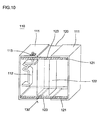
- As FIG. 10 shows, a
conventional filter 110 comprises adielectric resonant device 120,metal panels 111 having anexternal connector 113 that serves as an input-output connecting means and covers open portions of thedielectric resonant device 120, and acoupling loop 112. - The
dielectric resonant device 120 includes aframe 121 and adielectric resonator 122 that are made of ceramic. Theframe 121 is shaped like a parallelepiped with two opposing surfaces being open, and is provided withconductors 123 thereon. Thedielectric resonator 122 is shaped like a rectangular parallelepiped, and is disposed inside theframe 121 so that its two opposing surfaces are integrated with theframe 121. Themetal panels 111 are made of metal, such as iron or a nickel alloy, in order to achieve good electrical conductivity and to make the coefficient of linear expansion thereof the same as that of a dielectric. Thesemetal panels 111 are connected to theconductors 123 of the dielectricresonant device 120, whereby acavity 130 is formed as a whole. - The
coupling loop 112 is made of copper in view of electrical conductivity and rust prevention, and worked into the shape of an L. One end of thecoupling loop 112 fits in a hole that is previously formed through themetal panel 111, and is fixed by soldering or the like. The other end of thecoupling loop 112 is connected to theexternal connector 113. Since this other end of thecoupling loop 112 is also worked into a corrugated shape, it can, for example, absorb impact that is applied from the side of theexternal connector 113. This has solved problems, for example, deformation of thecoupling loop 112 due to stress from the outside, and separation of thecoupling loop 112 from themetal panel 111. - In the
filter 110 mentioned above, current applied from the outside flows in thecoupling loop 112 via theexternal connector 113. The current that flows through thecoupling loop 112 generates a magnetic field, and this magnetic field couples with thedielectric resonator 122. In this case, the degree of coupling between thecoupling loop 112 and thedielectric resonator 122 is adjusted based on the length, thickness, and width of thecoupling loop 112 or the distance between thecoupling loop 112 and thedielectric resonator 122. Such adjustment of the degree of coupling allows a filter having the required electrical characteristics. - A coupling loop has its own natural frequency, and the natural frequency of a coupling loop in a conventional filter is about 260Hz. On the other hand, in normal use of the filter, a device itself, in which the filter is incorporated, vibrates with the vibrations applied from the outside. In this case, frequencies ranging from about 5Hz to 200Hz are a problem. There is a likelihood that a coupling loop will resonate with the vibrations from the outside. The coupling loop resonates because the frequency of the external vibrations is almost equivalent to the natural frequency of the coupling loop. Although the natural frequency of the conventional coupling loop does not coincide with the frequency of the external vibrations, if it remains about 260Hz, the attenuation amount is not sufficient near about 200Hz, which is an unnecessary signal, thereby affecting the filter characteristics to a degree that is not disregarded. As the coupling loop resonates with the external vibrations, the degree of coupling between the coupling loop and the dielectric resonator varies, and the electrical characteristics, such as return loss, are thereby disturbed. Moreover, reliability of the filter is deteriorated.
- In order to solve the above problems, it may be possible to further increase the natural frequency of the coupling loop so that the resonance with the external vibrations can be disregarded. Incidentally, the coupling loop can be regarded as having a beam structure. In general, the natural frequency of a beam is expressed by the following formula:
- Referring to the above formula, it may be possible to reduce the length of the beam in order to increase the natural frequency of the coupling loop. Since the length of the beam has an influence on the degree of coupling with the dielectric resonator, however, it cannot be easily changed. Accordingly, it is good, in practice, to change the bending rigidity of the beam. The bending rigidity of the beam is given by the product of the Young's modulus and the second moment of area of the material. Therefore, the bending rigidity of the beam can be improved by increasing the Young's modulus or the second moment of area of the material. Although iron is available as a material having a high Young's modulus, the use of iron for the coupling loop causes a new problem, that is, thorough rust prevention is required. When the coupling loop is made of iron, in general, intermodulation (IM) is apt to occur, and therefore, the coupling loop is plated with silver. If the silver plate rusts, however, iron appears on the surface thereof, and IM is likely to occur. Although it may also be possible to increase the thickness of the coupling loop in order to increase the second moment of area, this results in an increase in the material cost.
- The coupling loop is formed by bending a metal plate into the shape of an L. Therefore, the strength of the bent portion is low, and this leads to a fear that the positional relationship between the coupling loop and the dielectric resonator may change.
- Furthermore, one end of the coupling loop on the side of the external connector has been heretofore corrugated so as to absorb impact from the external connector. It is, however, not so easy to corrugate an end of the coupling loop, and costs become high.
- FR 2118859 A concerns a cavity resonator having a coupling loop extending from an input/output connector to the inside of the cavity. Instead of forming the entire loop by a wire-shaped conductor, the loop is formed by a first portion of a wire-shaped conductor extending from the connector and by two thin conductive plates arranged substantially perpendicular to each other and extending from the end of the wire-shaped conductor to a wall of the cavity.
- US-A-5,625,330 describes a resonator coupling device having a rotatable ring for adjusting the loaded Q. The coupling device consists of a connector, a ring and a coupling loop extending into the interior of a resonator cavity. The loop is electrically and mechanically connected to a central conductor and is formed from a strip of sheet metal with one end connected to the central conductor and the other end being soldered in a slot of the coupling device.
- It is the object of the present invention to provide an improved filter hardly being effected by vibrations applied from the outside and having a high reliability.
- This object is achieved by a filter according to
claim 1. - According to a further aspect, the present invention provides for a duplexer using the inventive filter and according to yet a further aspect, the present invention concerns a communication device having such a duplexer using the inventive filter.
- According to an aspect of the present invention, there is provided a filter having a cavity, an input-output connecting means mounted in the cavity, and a coupling loop connected to the input-output connecting means so as to couple with a magnetic field inside the cavity, wherein a rib is formed on the coupling loop for increasing the natural frequency thereof.
- According to another aspect of the present invention, the coupling loop is formed by bending a metal plate along a bending line, and the rib extends in a direction that is not in parallel with the bending line.
- According to a further aspect of the present invention, the coupling loop includes a section having high rigidity and a curved section having low rigidity, one end of the high-rigidity section is connected to the cavity, the other end thereof is connected to one end of the low-rigidity curved section, and the other end of the low-rigidity curved section is connected to the input-output connecting means.
- Preferably, a dielectric resonator is disposed inside the cavity.
- Preferably, a rib is formed in a bent portion of the coupling loop.
- This structure makes it possible to increase the natural frequency of the coupling loop, and to thereby prevent the coupling loop from resonating with vibrations from the outside. Moreover, it is possible to mechanically reinforce the bent portion of the coupling loop, and to limit the change of degree of coupling, whereby a reliable filter can be provided.
- Accordingly, it is possible to easily manufacture at low cost a coupling loop that is connected to an external connector and that absorbs impact applied through the external connector. In addition, it is possible to provide a reliable filter in which change of degree of coupling is prevented.
- According to a further aspect of the present invention, there is provided a duplexer including at least two filters, input-output connecting means connected to the filters, and an antenna connecting means commonly connected to the filters, wherein at least one of the filters is a filter of the above-mentioned type.
- According to a still further aspect of the present invention, there is provided a communication device including the above-mentioned duplexer, a transmission circuit connected to at least one of the input-output connecting means in the duplexer, a receiving circuit connected to at least one of the input-output connecting means that differs from the input-output connecting means connected to the transmission circuit, and an antenna connected to the antenna connecting means in the duplexer.
- According to the above, it is possible to obtain a duplexer and a communication device having stable properties and high reliability.
- Further objects, features and advantages of the present invention will become apparent from the following description of the preferred embodiments with reference to the attached drawings.
-
- FIG. 1 is a perspective view of a filter according to the present invention;
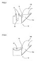
- FIG. 2 is a perspective view of a coupling loop shown in FIG. 1;
- FIG. 3 is a perspective view showing another example of a coupling loop according to the present invention;
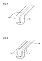
- FIG. 4 is a perspective view showing only a high-rigidity section of a further example of a coupling loop according to the present invention;
- FIG. 5 is a perspective view showing only a high-rigidity section of a further example of a coupling loop according to the present invention;
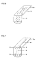
- FIG. 6 is a perspective view showing only a high-rigidity section of a further example of a coupling loop according to the present invention;
- FIG. 7 is a perspective view showing only a high-rigidity section of a further example of a coupling loop according to the present invention;
- FIG. 8 is an equivalent circuit diagram of a duplexer according to the present invention;
- FIG. 9 is a schematic view of a communication device according to the present invention; and
- FIG. 10 is a perspective view of a conventional filter.
-
- A filter according to an embodiment of the present invention will be described below with reference to the attached drawings. A dielectric resonant device in this embodiment is of a type in which a dielectric resonator is disposed inside a frame.
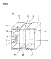
- FIG. 1 is a schematic perspective view of the filter according to the present invention. In FIG. 1, the filter is cut along the plane perpendicular to the open surface of a dielectric
resonant device 20, in order for the inside thereof to be seen well. Although couplingloops 12, andexternal connectors 13 that serve as input-output connecting means are provided for input and output, since they have the same structure, only one of thecoupling loops 12 and one of theexternal connectors 13 are illustrated and described. - The
filter 10 generally comprises a TM mode dielectricresonant device 20, andmetal panels 11 mounted to cover open portions of the dielectricresonant device 20. - In the TM mode dielectric
resonant device 20, adielectric resonator 22 made of ceramic and shaped like a column is disposed inside aframe 21 that is also made of ceramic, andconductors 23 are formed by applying and baking silver paste on theframe 21. - The
metal panels 11, which are mounted at the open portions of the dielectricresonant device 20, are worked from a metal plate of iron, a nickel alloy, or the like, by pressing or stamping, and are provided with thecoupling loop 12 and theexternal connector 13. Themetal panels 11 are soldered so as to cover the open portions of the dielectricresonant device 20, and connected to theconductors 23 of the dielectricresonant device 20, whereby acavity 30 is formed as a whole. - A metal cover is further mounted on the
filter 10, though it is not shown in FIG. 1, to maintain stability in installation, to prevent impact from being transmitted from the outside to the inside, and to mechanically reinforce an external connector section. - The
coupling loop 12 including a section havinghigh rigidity 12a and a section havinglow rigidity 12b. The high-rigidity section 12a is formed by bending a metal plate of copper or the like into the shape of an L. In contrast, the low-rigidity section 12b is formed by curving a metal plate that is made of phosphor bronze or the like and that has a smaller thickness than that of the high-rigidity section 12a, so that it has flexibility. - A
rib 14 is formed in a part of the high-rigidity section 12a that is parallel to themetal panel 11 so as to increase the second moment of area. - The high-
rigidity section 12a also has acutout portion 16 at one end thereof, as shown in FIG. 2, so that elastic force acts on the force exerted from the widthwise direction of thecutout portion 16. Moreover, two projectingportions 15 are formed to sandwich thecutout portion 16. Themetal panel 11 has a hole whose bore is smaller than the width of the two projectingportions 15. By being inserted in this hole formed through themetal panel 11, the projectingportions 15 of the high-rigidity section 12a are retained from both sides. Then, the projectingportions 15 are temporarily attached by using the elastic force to expand, and are fixed by soldering. The high-rigidity section 12a has a hole at the other end. One end portion of the low-rigidity section 12b is inserted in the hole, bent, and fixed by soldering. The other end of the low-rigidity section 12b also has a hole, in which the leading end of a center conductor of theexternal connector 13 is fixedly inserted. - One end of the high-
rigidity section 12a that is connected to themetal panel 11 may be further bent into the shape of an L so that a surface having ahole 17 is formed to be bonded to themetal panel 11, as shown in FIG. 3. In this case, a projection is formed on themetal panel 11 by stamping or louvering themetal panel 11 inward. The projection of themetal panel 11 is inserted in thehole 17, bent, and fixed by soldering. This simplifies the operation and improves stability of the bonded portion. - FIGS. 4 to 7 demonstrate variations of the
rib 14, and each shows only the high-rigidity section 12a of thecoupling loop 12 that is worked into the shape of an L and fixed to themetal panel 11. - In the variation shown in FIG. 4, a
rib 14 is also formed in a part of the high-rigidity section 12a in thecoupling loop 12, which is nearly perpendicular to themetal panel 11, so that it extends in the direction nearly perpendicular to themetal panel 11, thereby further increasing the natural frequency. - There may be provided a plurality of
ribs 14, as shown in FIG. 5. In this case, the natural frequency of thecoupling loop 12 can be further increased. - When the
rib 14 is shaped like a cross, as shown in FIG. 6, it is possible to increase the strength of thecoupling loop 12 with respect to vibrations in other directions. - As shown in FIG. 7,
ribs 19 may be formed in bent portions of the high-rigidity section 12a of thecoupling loop 12. This makes it possible to increase the mechanical strength of the bent portions, to prevent a change in the bending angle of thecoupling loop 12, and to prevent a change in the degree of coupling between thecoupling loop 12 and thedielectric resonator 22. As a result, a filter having high reliability can be provided. - While the filter of this embodiment employs a dielectric resonant device in which a dielectric resonator shaped like a column is disposed inside a ceramic frame, the present invention is not limited to the illustrated embodiment. The present invention may also be applied to, for example, a filter using a double-mode or multiple-mode dielectric resonant device in which a cross-shaped dielectric resonator is placed.
- The present invention may also be applied to any device using a coupling loop, for example, a waveguide filter in which a coupling loop is mounted in a metal cavity.
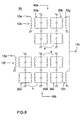
- Next, a duplexer according to an embodiment of the present invention will be described with reference to FIG. 8. FIG. 8 is an equivalent circuit diagram of the duplexer of this embodiment.
- As shown in FIG. 8, a
duplexer 35 of this embodiment comprises a four-stage transmission filter 40a composed of two double-mode dielectricresonant devices stage receiving filter 40b composed of three double-mode dielectricresonant devices resonant devices 20a to 20e used in thetransmission filter 40a and the receivingfilter 40b, a cross-shaped dielectric resonator is placed in a frame having a conductor formed on the outer surface thereof, and two modes are coupled by forming a cutout for coupling at an intersection of the dielectric resonator, or other methods. - A metal panel is mounted at an open portion of each of the dielectric
resonant devices 20a to 20e so that it covers the open portion, and is provided with a coupling loop having the shape that has been described in the above embodiments. Coupling loops 12E and 12F, which are coupled to the first stage of thetransmission filter 40a and the last stage of the receivingfilter 40b, respectively, are connected toexternal connectors transmission filter 40a and the first stage of the receivingfilter 40b are commonly connected to a singleexternal connector 13c. On the other hand, coupling loops are mounted between the second and third stages of thetransmission filter 40a, between the second and third stages of the receivingfilter 40b, and between the fourth and fifth stages of the receivingfilter 40b in order to couple the dielectric resonant devices. A line, such as a coaxial line, connected to theexternal connector 13a, to which the coupling loop 12E coupled with the first stage of thetransmission filter 40a is connected, is connected to an external transmission circuit, and a line connected to theexternal connector 13b, to which the coupling loop 12F coupled to the last stage of the receivingfilter 40b is connected, is connected to an external receiving circuit. Furthermore, a line connected to theexternal connector 13c, to which the coupling loops 12G and 12H coupled to the last stage of thetransmission filter 40a and the first stage of the receivingfilter 40b are commonly connected, is connected to an antenna. - In the
duplexer 35 having such a configuration, a signal having a predetermined frequency, of signals input from the external transmission circuit to thetransmission filter 40a, is output to the antenna, and a signal having a predetermined frequency, which is different from the aforesaid frequency, of signals input from the antenna to the receivingfilter 40b, is output to the external receiving circuit. - Furthermore, a communication device according to an embodiment of the present invention will be described with reference to FIG. 9. FIG. 9 is a schematic view of the communication device of this embodiment.
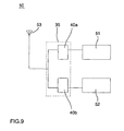
- As shown in FIG. 9, a
communication device 50 of this embodiment comprises aduplexer 35, atransmission circuit 51, a receivingcircuit 52, and anantenna 53. Theduplexer 35 is the same as that described in the above embodiment. The coupling loop 12E coupled to the first stage of thetransmission filter 40a is connected to thetransmission circuit 51 via theexternal connector 13a and the line, and the coupling loop 12F coupled to the last stage of the receivingfilter 40b is connected to the receivingcircuit 52 via theexternal connector 13b and the line. Moreover, the coupling loop 12C coupled to the last stage of thetransmission filter 40a and the coupling loop 12H coupled to the first stage of the receivingfilter 40b are connected to theantenna 53 via theexternal connector 13c and the line. - In the duplexer and the communication device mentioned in the above embodiments, since the natural frequency of the coupling loop is apart from the frequency that has been a problem, the properties are stabilized, thereby improving reliability.
- As mentioned above, according to the present invention, the natural frequency of the coupling loop is increased by forming a rib in the coupling loop, for example, increased to about 380Hz in the case in which a single rib is formed, as shown in FIG. 1. This allows a satisfactory attenuation amount near 200Hz. The resonation resulting from the external vibration, which has been a problem hitherto, can be reduced to a negligible degree, thereby preventing the electrical characteristics, such as return loss, from being disturbed. As a result, it is possible to provide a filter having high reliability.
- Furthermore, the bent portion of the coupling loop can be mechanically reinforced by a rib formed therein. As a result, it is possible to further improve stability of the coupling loop, and to prevent a change in the degree of coupling between the coupling loop and the electromagnetic field generated in the cavity.
- Still furthermore, the coupling loop including two sections, an L-shaped section having high rigidity, and a curved section having low rigidity. One end of the high-rigidity L-shaped section is connected to the cavity, the other end thereof is connected to one end of the low-rigidity curved section, and the other end of the low-rigidity curved section is connected to the external connector. This permits the low-rigidity section of the coupling loop to absorb impact from the external connector. Consequently, it is possible to provide a filter having stable characteristics.
Claims (7)
- A filter (10) having a cavity (30), input-output connecting means (13) mounted in said cavity (30), and a coupling loop (12) connected to said input-output connecting means (13) so as to couple with a magnetic field inside said cavity (30),
characterized in that
said coupling loop (12) comprises a rib (14) formed on said coupling loop (12) for increasing the natural frequency thereof. - A filter (10) according to claim 1, wherein said coupling loop (12) is formed by bending a metal plate along a bending line, and said rib (14) extends in a direction that is not in parallel with said bending line.
- A filter (10) according to claim 1 or 2, wherein said coupling loop (12) includes a section (12a) having high rigidity and a curved section (12b) having low rigidity, one end of said high-rigidity section (12a) is connected to said cavity (30), the other end thereof is connected to one end of said low-rigidity curved section (12b), and the other end of said low-rigidity curved section (12b) is connected to said input-output connecting means (13), and said rib (14) is formed on said section (12a) having high rigidity.
- A filter (10) according to claim 2 or 3, wherein said rib (14) is formed on a bent portion of said coupling loop (12).
- A filter (10) according to one of claims 1 to 4, wherein a dielectric resonator (20) is disposed inside said cavity (30).
- A duplexer (35) comprising:wherein at least one of said filters (40a, 40b) is a filter (10) according to any of claims 1 to 5.at least two filters (40a, 40b);input-output connecting means (13a, 13b) connected to said filters (40a, 40b); andantenna connecting means (13c) commonly connected to said filters (40a, 40b),
- A communication device (50) comprising:a duplexer (35) according to claim 6;a transmission circuit (51) connected to at least one of input-output connecting means (13a) in said duplexer (35);a receiving circuit (52) connected to at least one of said input-output connecting means (13b) that differs from said input-output connecting means (13a) connected to said transmission circuit (51); andan antenna (53) connected to antenna connecting means (13c) in said duplexer (35).
Applications Claiming Priority (5)
| Application Number | Priority Date | Filing Date | Title |
|---|---|---|---|
| JP302647/97 | 1997-11-05 | ||
| JP30264797 | 1997-11-05 | ||
| JP30264797 | 1997-11-05 | ||
| US09/186,512 US6377132B1 (en) | 1997-11-05 | 1998-11-04 | Filter, duplexer, and communication device |
| CN98123981A CN1223478A (en) | 1997-11-05 | 1998-11-05 | Filter, duplexer, and communication device |
Publications (2)
| Publication Number | Publication Date |
|---|---|
| EP0917239A1 EP0917239A1 (en) | 1999-05-19 |
| EP0917239B1 true EP0917239B1 (en) | 2005-05-04 |
Family
ID=27179222
Family Applications (1)
| Application Number | Title | Priority Date | Filing Date |
|---|---|---|---|
| EP98120842A Expired - Lifetime EP0917239B1 (en) | 1997-11-05 | 1998-11-03 | Filter, duplexer and communication device |
Country Status (4)
| Country | Link |
|---|---|
| US (1) | US6377132B1 (en) |
| EP (1) | EP0917239B1 (en) |
| CN (1) | CN1223478A (en) |
| NO (1) | NO317453B1 (en) |
Families Citing this family (5)
| Publication number | Priority date | Publication date | Assignee | Title |
|---|---|---|---|---|
| JP3883902B2 (en) * | 2002-04-25 | 2007-02-21 | 三洋電機株式会社 | Dielectric filter |
| SE0301200D0 (en) * | 2003-04-24 | 2003-04-24 | Amc Centurion Ab | Antenna device and portable radio communication device including such an antenna device |
| NL1027304C2 (en) * | 2004-10-20 | 2006-04-24 | Mecal Applied Mechanics B V | Support structure, fixation member and method. |
| KR100703719B1 (en) * | 2005-07-26 | 2007-04-06 | 한국전자통신연구원 | Filter coupled by the conductive plates with a curved surface |
| CN104701592B (en) * | 2015-04-01 | 2017-11-21 | 河南理工大学 | TM mould medium cavity body filters |
Family Cites Families (7)
| Publication number | Priority date | Publication date | Assignee | Title |
|---|---|---|---|---|
| FR2118859A1 (en) * | 1970-12-23 | 1972-08-04 | Thomson Varian | |
| JPH0622282B2 (en) * | 1987-05-29 | 1994-03-23 | 株式会社村田製作所 | Outer coupling structure of dielectric resonator and outer coupling adjusting method using the same |
| US5004992A (en) * | 1990-05-25 | 1991-04-02 | Motorola, Inc. | Multi-resonator ceramic filter and method for tuning and adjusting the resonators thereof |
| NZ248549A (en) * | 1993-08-31 | 1997-01-29 | Deltec New Zealand | Loop coupler for resonator: rotates to adjust loaded q |
| JP3344102B2 (en) * | 1994-09-13 | 2002-11-11 | 株式会社村田製作所 | Magnetic field coupling input / output device and dielectric resonator |
| JP3050099B2 (en) * | 1995-09-01 | 2000-06-05 | 株式会社村田製作所 | Dielectric filter and antenna duplexer |
| AUPO076796A0 (en) * | 1996-07-01 | 1996-07-25 | Jacobs, Ian Orde Michael | Injection moulding |
-
1998
- 1998-11-03 EP EP98120842A patent/EP0917239B1/en not_active Expired - Lifetime
- 1998-11-04 NO NO19985147A patent/NO317453B1/en not_active IP Right Cessation
- 1998-11-04 US US09/186,512 patent/US6377132B1/en not_active Expired - Lifetime
- 1998-11-05 CN CN98123981A patent/CN1223478A/en active Pending
Also Published As
| Publication number | Publication date |
|---|---|
| EP0917239A1 (en) | 1999-05-19 |
| NO985147D0 (en) | 1998-11-04 |
| NO317453B1 (en) | 2004-11-01 |
| US6377132B1 (en) | 2002-04-23 |
| NO985147L (en) | 1999-05-06 |
| CN1223478A (en) | 1999-07-21 |
Similar Documents
| Publication | Publication Date | Title |
|---|---|---|
| US6337663B1 (en) | Built-in dual frequency antenna | |
| EP1164655A2 (en) | Resonator and high-frequency filter | |
| WO2002058185A1 (en) | High frequency circuit element and high frequency circuit module | |
| EP0928039A1 (en) | Band elimination dielectric filter, dielectric duplexer and communication device using the same | |
| US6236291B1 (en) | Dielectric filter, duplexer, and communication device | |
| JP3531570B2 (en) | Resonator, filter, duplexer, communication equipment | |
| EP0917239B1 (en) | Filter, duplexer and communication device | |
| US6529094B1 (en) | Dielectric resonance device, dielectric filter, composite dielectric filter device, dielectric duplexer, and communication apparatus | |
| CA2252364C (en) | Filter, duplexer, and communication device | |
| KR100365452B1 (en) | Dielectric filter, dielectric duplexer, and communication device | |
| JP3013798B2 (en) | Crossing track | |
| EP1143552A1 (en) | Sheet-metal filter | |
| KR100470312B1 (en) | Dielectric resonator device, filter, duplexer, and communication device | |
| EP0477925A1 (en) | Dielectric resonator device | |
| JPH11312904A (en) | Filter, duplexer and communication equipment | |
| JP3624679B2 (en) | Dielectric filter, duplexer and communication device | |
| US6150906A (en) | HF filter using resonators having convex-concave structure | |
| JP3444218B2 (en) | Dielectric resonator, dielectric filter, dielectric duplexer, oscillator, communication device | |
| JP3512180B2 (en) | High frequency circuit element and high frequency circuit module | |
| US6538533B1 (en) | Dielectric resonator filter | |
| JP3392397B2 (en) | High frequency filter | |
| JP2002158514A (en) | Resonator and high-frequency filter | |
| JP3385660B2 (en) | Waveguide type resonator device | |
| JP4103330B2 (en) | NRD guide L type antenna element | |
| JPS5947804A (en) | Dielectric filter |
Legal Events
| Date | Code | Title | Description |
|---|---|---|---|
| PUAI | Public reference made under article 153(3) epc to a published international application that has entered the european phase |
Free format text: ORIGINAL CODE: 0009012 |
|
| 17P | Request for examination filed |
Effective date: 19981103 |
|
| AK | Designated contracting states |
Kind code of ref document: A1 Designated state(s): DE FI FR GB IT NL SE |
|
| AX | Request for extension of the european patent |
Free format text: AL;LT;LV;MK;RO;SI |
|
| AKX | Designation fees paid |
Free format text: DE FI FR GB IT NL SE |
|
| 17Q | First examination report despatched |
Effective date: 20030812 |
|
| GRAP | Despatch of communication of intention to grant a patent |
Free format text: ORIGINAL CODE: EPIDOSNIGR1 |
|
| GRAS | Grant fee paid |
Free format text: ORIGINAL CODE: EPIDOSNIGR3 |
|
| GRAA | (expected) grant |
Free format text: ORIGINAL CODE: 0009210 |
|
| AK | Designated contracting states |
Kind code of ref document: B1 Designated state(s): DE FI FR GB IT NL SE |
|
| PG25 | Lapsed in a contracting state [announced via postgrant information from national office to epo] |
Ref country code: NL Free format text: LAPSE BECAUSE OF FAILURE TO SUBMIT A TRANSLATION OF THE DESCRIPTION OR TO PAY THE FEE WITHIN THE PRESCRIBED TIME-LIMIT Effective date: 20050504 Ref country code: IT Free format text: LAPSE BECAUSE OF FAILURE TO SUBMIT A TRANSLATION OF THE DESCRIPTION OR TO PAY THE FEE WITHIN THE PRE;WARNING: LAPSES OF ITALIAN PATENTS WITH EFFECTIVE DATE BEFORE 2007 MAY HAVE OCCURRED AT ANY TIME BEFORE 2007. THE CORRECT EFFECTIVE DATE MAY BE DIFFERENT FROM THE ONE RECORDED.SCRIBED TIME-LIMIT Effective date: 20050504 Ref country code: FI Free format text: LAPSE BECAUSE OF FAILURE TO SUBMIT A TRANSLATION OF THE DESCRIPTION OR TO PAY THE FEE WITHIN THE PRESCRIBED TIME-LIMIT Effective date: 20050504 |
|
| REG | Reference to a national code |
Ref country code: GB Ref legal event code: FG4D |
|
| REF | Corresponds to: |
Ref document number: 69830035 Country of ref document: DE Date of ref document: 20050609 Kind code of ref document: P |
|
| PG25 | Lapsed in a contracting state [announced via postgrant information from national office to epo] |
Ref country code: SE Free format text: LAPSE BECAUSE OF FAILURE TO SUBMIT A TRANSLATION OF THE DESCRIPTION OR TO PAY THE FEE WITHIN THE PRESCRIBED TIME-LIMIT Effective date: 20050804 |
|
| NLV1 | Nl: lapsed or annulled due to failure to fulfill the requirements of art. 29p and 29m of the patents act | ||
| PLBE | No opposition filed within time limit |
Free format text: ORIGINAL CODE: 0009261 |
|
| STAA | Information on the status of an ep patent application or granted ep patent |
Free format text: STATUS: NO OPPOSITION FILED WITHIN TIME LIMIT |
|
| ET | Fr: translation filed | ||
| 26N | No opposition filed |
Effective date: 20060207 |
|
| REG | Reference to a national code |
Ref country code: FR Ref legal event code: PLFP Year of fee payment: 18 |
|
| REG | Reference to a national code |
Ref country code: FR Ref legal event code: PLFP Year of fee payment: 19 |
|
| REG | Reference to a national code |
Ref country code: FR Ref legal event code: PLFP Year of fee payment: 20 |
|
| PGFP | Annual fee paid to national office [announced via postgrant information from national office to epo] |
Ref country code: FR Payment date: 20171121 Year of fee payment: 20 Ref country code: DE Payment date: 20171121 Year of fee payment: 20 |
|
| PGFP | Annual fee paid to national office [announced via postgrant information from national office to epo] |
Ref country code: GB Payment date: 20171123 Year of fee payment: 20 |
|
| REG | Reference to a national code |
Ref country code: DE Ref legal event code: R071 Ref document number: 69830035 Country of ref document: DE |
|
| REG | Reference to a national code |
Ref country code: GB Ref legal event code: PE20 Expiry date: 20181102 |
|
| PG25 | Lapsed in a contracting state [announced via postgrant information from national office to epo] |
Ref country code: GB Free format text: LAPSE BECAUSE OF EXPIRATION OF PROTECTION Effective date: 20181102 |