EP0914717B1 - Digital-analog- und analog-digital-wandler - Google Patents
Digital-analog- und analog-digital-wandler Download PDFInfo
- Publication number
- EP0914717B1 EP0914717B1 EP98915053A EP98915053A EP0914717B1 EP 0914717 B1 EP0914717 B1 EP 0914717B1 EP 98915053 A EP98915053 A EP 98915053A EP 98915053 A EP98915053 A EP 98915053A EP 0914717 B1 EP0914717 B1 EP 0914717B1
- Authority
- EP
- European Patent Office
- Prior art keywords
- digital
- analogue
- converter
- current
- mosfet
- Prior art date
- Legal status (The legal status is an assumption and is not a legal conclusion. Google has not performed a legal analysis and makes no representation as to the accuracy of the status listed.)
- Expired - Lifetime
Links
- 238000005513 bias potential Methods 0.000 claims description 3
- 230000000295 complement effect Effects 0.000 claims description 2
- 210000004027 cell Anatomy 0.000 description 6
- 230000001419 dependent effect Effects 0.000 description 4
- 238000013461 design Methods 0.000 description 4
- 238000000034 method Methods 0.000 description 4
- 210000000352 storage cell Anatomy 0.000 description 4
- 230000005669 field effect Effects 0.000 description 3
- 238000012986 modification Methods 0.000 description 3
- 230000004048 modification Effects 0.000 description 3
- 230000003071 parasitic effect Effects 0.000 description 3
- 230000008569 process Effects 0.000 description 3
- 238000010586 diagram Methods 0.000 description 2
- 230000006870 function Effects 0.000 description 2
- 238000012545 processing Methods 0.000 description 2
- 238000005070 sampling Methods 0.000 description 2
- 230000003068 static effect Effects 0.000 description 2
- 230000008859 change Effects 0.000 description 1
- 238000012886 linear function Methods 0.000 description 1
- 230000009467 reduction Effects 0.000 description 1
- 230000004044 response Effects 0.000 description 1
- 238000007493 shaping process Methods 0.000 description 1
- 238000012546 transfer Methods 0.000 description 1
Images


Classifications
-
- H—ELECTRICITY
- H03—ELECTRONIC CIRCUITRY
- H03M—CODING; DECODING; CODE CONVERSION IN GENERAL
- H03M1/00—Analogue/digital conversion; Digital/analogue conversion
- H03M1/06—Continuously compensating for, or preventing, undesired influence of physical parameters
- H03M1/0617—Continuously compensating for, or preventing, undesired influence of physical parameters characterised by the use of methods or means not specific to a particular type of detrimental influence
- H03M1/0675—Continuously compensating for, or preventing, undesired influence of physical parameters characterised by the use of methods or means not specific to a particular type of detrimental influence using redundancy
- H03M1/0678—Continuously compensating for, or preventing, undesired influence of physical parameters characterised by the use of methods or means not specific to a particular type of detrimental influence using redundancy using additional components or elements, e.g. dummy components
-
- H—ELECTRICITY
- H03—ELECTRONIC CIRCUITRY
- H03M—CODING; DECODING; CODE CONVERSION IN GENERAL
- H03M1/00—Analogue/digital conversion; Digital/analogue conversion
-
- H—ELECTRICITY
- H03—ELECTRONIC CIRCUITRY
- H03M—CODING; DECODING; CODE CONVERSION IN GENERAL
- H03M1/00—Analogue/digital conversion; Digital/analogue conversion
- H03M1/66—Digital/analogue converters
-
- H—ELECTRICITY
- H03—ELECTRONIC CIRCUITRY
- H03M—CODING; DECODING; CODE CONVERSION IN GENERAL
- H03M1/00—Analogue/digital conversion; Digital/analogue conversion
- H03M1/66—Digital/analogue converters
- H03M1/74—Simultaneous conversion
- H03M1/742—Simultaneous conversion using current sources as quantisation value generators
Definitions
- the invention relates to a digital to analogue converter.
- the invention further relates to an analogue to digital converter.
- the invention has particular, though not exclusive, application in sigma delta converters.
- the feedback D/A converter presents its signal output to the input of the first integrator (or possibly differentiator) in the noise shaping filter.
- Signal summation i.e. of the input and feedback currents, is achieved by simple connection of wires.
- switched current circuits there is always a settling error due to the time constant formed primarily by the total load capacitance at the summing node and the g m of the storage MOS transistor. Account is normally taken of this in the design and organisation of the storage cells. Any settling error should ideally be very small in absolute terms as there may be a non-linear relationship between the proportion of the error and the incoming signal. Such a variation of settling error will manifest itself as distortion in the signal.
- the most convenient form for a current mode D/A converter is to use current sources (or sinks) comprising appropriately biassed MOS transistors which are selectively switched to a current summing node under the control of the applied digital code.
- Each of these current sources has its own parasitic capacitance to ground, principally due to the drain-bulk capacitances of the MOS transistors.
- the total capacitance at the summing node (which also forms the input node of the A/D converter) is a function of the applied digital code. Consequently there is a corresponding variation in the settling time of the first integrator and hence a code dependent settling error in the signal stored. This presents a serious risk of distortion, especially in a design optimised for high sample rates where settling time is traded with acceptable sampling error with some precision.
- the invention provides a digital to analogue converter including a plurality of current sources each connected to a common node forming an output of the digital to analogue converter via a respective switch whose state is controlled in accordance with an applied digital code to be converted, the digital to analogue converter further including a corresponding plurality of dummy current sources which produce substantially zero current but which have an associated capacitance substantially equal to that of their corresponding current source, each of the dummy current sources being connected to the common node via further respective switches, the state of each of the further respective switches being controlled in accordance with the logical complement of the applied digital code.
- the measures adopted according to the invention provide a D/A converter having a substantially constant capacitance at the summing node irrespective of the digital code to be converted.
- a sigma delta A/D converter there will not be any variation in settling error with instantaneous digital code and it becomes possible to optimise the trade-offs in switched current storage cells for a known load capacitance.
- all the current sources may have the same value. This arrangement is convenient for multi-bit sigma delta converters since it can operate directly on the thermometer code produced naturally by the quantiser.
- Each current source may comprise an MOSFET having its gate electrode connected to a bias potential source.
- the D/A converter conveniently comprises a plurality of unit sized MOS transistors biassed from a common reference so that a plurality of identical currents may be added to the output via digitally controlled switches.
- the dummy current source may comprise a further MOSFET having the same dimensions as the corresponding current source MOSFET, the further MOSFET being biased to be non-conducting.
- the invention further provides a sigma-delta analogue to digital converter including such a digital to analogue converter.
- the A/D converter may be arranged to process differential input currents and include first and second such D/A converters.
- the A/D converter includes a noise shaper using switched current circuits for the signal processing a constant node capacitance is presented to the storage cell input and hence there is no code dependent change in settling time due to changing node capacitance,
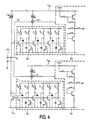
- Figure 1 shows in schematic form a digital to analogue converter according to the invention which produces an analogue output current whose value depends upon an applied digital code.
- the digital to analogue converter is shown in Figure 1 comprises a current source 1, which supplies a reference current I ref and is connected between a supply rail V dd and the drain and gate electrodes of an N-channel field effect transistor T ref .
- the source electrode of the transistor T ref is connected to a supply rail V ss.
- the gate electrode of transistor T ref is connected to the gate electrodes of a plurality of transistors T 0 ,T 1 ,...T N .
- the source electrodes of transistors T 0 to T N are connected to the supply rail V ss , while their drain electrodes are connected via respective switches D 0 , D 1 ...D N to a line 2 which is connected to an output 3 of the digital to analogue converter.
- a further current source 4 is connected between the supply rail V dd and the line 2 to act as a bias and a current offset so that the total output current can be in either direction.
- a further plurality of transistors T o , T l ??. T N have their gate and source electrodes connected to the supply rail V ss .
- the drain electrodes of transistors T o , T l , ............ T n are connected via respective switches D o , D l . « D N to the line 2.
- Each of the current sources consisting of transistors T 0 to T N respectively has its own parasitic capacitance to ground C O to C N principally due to drain bulk capacitances. If we initially neglect the contribution of transistors T O , T I ?? T N and switches D O , D I .» D N the total capacitance at the output 3 will be an approximately linear function of the digital code. If such an output is connected to the input of a switched current integrator it will cause a consequent variation in the settling time constant of that integrator and hence a code dependent settling error in the signals stored. This presents a serious risk of distortion particularly in a design optimised for very high sample rates where the settling time must be traded for acceptable sampling error with some precision.
- transistors T 0 to T N and switches D N to D O are provided.
- the transistors T 0 to T N have associated capacitances C 0 to C N which are substantially equal to the capacitances C 0 to C N.
- the switches D 0 to D N are operated by the inverse binary code to that which operates the switches D 0 to D N.
- the transistors T 0 to T N do not provide any contribution to the current output of the D/A converter as they are non-conducting but their associated capacitances are selectively connected to ensure a constant total capacitance at the output 3.
- FIG. 2 shows a sigma delta analogue to digital converter according to the invention.
- the converter has an input 20 to which an input signal is fed and which is connected to the first input of a summing circuit 21.
- the output of a digital to analogue converter 22 is connected to a second input of the summing circuit 21.
- the digital to analogue converter 22 takes the form of that shown in Figure 1.
- the output of the summing circuit 21 is fed to a noise shaper 23 whose output is fed to a quantiser 24.
- the output of the quantiser 24 is fed to the input of the digital to analogue converter 22 and as an output digital code to an output 25.
- the noise shaper 23 may be comprised for example from switched current integrators. As is known, switched current integrators have an input which can sample the output current from the summing circuit 21.
- Figure 3 shows in further detail the interface between the input signal, the output of the digital to analogue converter and the noise shaper.
- the input 20 is fed to a first input of a current summing node 21 while the output of the digital to analogue converter 22 is fed to a second input of the current summing node 21.
- the output from the current summing node 21 is fed to the input of the noise shaper 23.
- the input of the noise shaper 23 comprises a switched current memory cell which samples the input during a first phase of a clock signal.
- the particular type of current memory cell shown as the input circuit of the noise shaper 23 is described in EP-A- 0 608 936
- the current summing network 21 may consist merely of a node to which the input current and the output current of the digital to analogue converter 22 are applied and the current flowing from the node flows into the input of the noise shaper 23.
- noise shaper 23 is constructed using switched current techniques as the response of any transconductance stage will be affected by the capacitance presented at its input.
Landscapes
- Engineering & Computer Science (AREA)
- Theoretical Computer Science (AREA)
- Analogue/Digital Conversion (AREA)
- Compression, Expansion, Code Conversion, And Decoders (AREA)
Claims (8)
- Digital-Analog-Wandler, welcher mehrere Stromquellen (T0 ... TN) aufweist, die über einen jeweiligen Schalter (D0 ... DN), dessen Zustand entsprechend einem umzusetzenden, angewandten Digitalcode gesteuert wird, jeweils mit einem, einen Ausgang (3) des Digital-Analog-Wandlers bildenden, gemeinsamen Knotenpunkt (2) verbunden sind, wobei der Digital-Analog-Wandler weiterhin eine entsprechend große Anzahl Blindstromquellen (
T 0 ...T N ) aufweist, welche praktisch Nullstrom erzeugen, jedoch eine zugeordnete Kapazität (C 0 ...C N ) vorsehen, welche im Wesentlichen dieser ihrer entsprechenden Stromquelle entspricht, wobei jede der Blindstromquellen (T 0 ...T N ) über weitere jeweilige Schalter (D 0 ...D N ) mit dem gemeinsamen Knotenpunkt (2) verbunden ist und wobei der Zustand jedes weiteren Schalters entsprechend dem logischen Komplement des angewandten Digitalcodes gesteuert wird. - Digital-Analog-Wandler nach Anspruch 1, wobei sämtliche Stromquellen der gleichen Wert aufweisen.
- Digital-Analog-Wandler nach Anspruch 1, wobei jede Stromquelle einen MOSFET aufweist, dessen Gate-Elektrode mit einer Vorspannungsquelle verbunden ist.
- Digital-Analog-Wandler nach Anspruch 2, wobei jede Stromquelle einen MOSFET aufweist, dessen Gate-Elektrode mit einer Vorspannungsquelle verbunden ist.
- Digital-Analog-Wandler nach Anspruch 3, wobei die Blindstromquelle (
T 0 ...T N ) einen weiteren MOSFET mit den gleichen Dimensionen wie der entsprechende Strom gesteuerte MOSFET aufweist, wobei der weitere MOSFET nicht leitend vorgespannt ist. - Digital-Analog-Wandler nach Anspruch 4, wobei die Blindstromquelle (
T 0 ...T N )einen weiteren MOSFET mit den gleichen Dimensionen wie der entsprechende Strom gesteuerte MOSFET (T0 ... TN) aufweist, wobei der weitere MOSFET nicht leitend vorgespannt ist. - Sigma-Delta-Analog-Digital-Wandler mit einem Digital-Analog-Wandler, wie in einem der vorangegangenen Ansprüche beansprucht.
- Sigma-Delta-Analog-Digital-Wandler zur Umwandlung eines analogen Differenzstromeingangs mit einem ersten und zweiten Digital-Analog-Wandler, wobei jeder Digital-Analog-Wandler wie in einem der Ansprüche 1 bis 6 beansprucht vorgesehen ist.
Applications Claiming Priority (3)
| Application Number | Priority Date | Filing Date | Title |
|---|---|---|---|
| GBGB9710658.7A GB9710658D0 (en) | 1997-05-24 | 1997-05-24 | Digital to analogue and analogue to digital converters |
| GB9710658 | 1997-05-24 | ||
| PCT/IB1998/000677 WO1998053555A2 (en) | 1997-05-24 | 1998-05-07 | Digital to analogue and analogue to digital converters |
Publications (2)
| Publication Number | Publication Date |
|---|---|
| EP0914717A2 EP0914717A2 (de) | 1999-05-12 |
| EP0914717B1 true EP0914717B1 (de) | 2003-08-06 |
Family
ID=10812936
Family Applications (1)
| Application Number | Title | Priority Date | Filing Date |
|---|---|---|---|
| EP98915053A Expired - Lifetime EP0914717B1 (de) | 1997-05-24 | 1998-05-07 | Digital-analog- und analog-digital-wandler |
Country Status (7)
| Country | Link |
|---|---|
| US (1) | US6104330A (de) |
| EP (1) | EP0914717B1 (de) |
| JP (1) | JP3850038B2 (de) |
| KR (1) | KR100539993B1 (de) |
| DE (1) | DE69816937T2 (de) |
| GB (1) | GB9710658D0 (de) |
| WO (1) | WO1998053555A2 (de) |
Families Citing this family (8)
| Publication number | Priority date | Publication date | Assignee | Title |
|---|---|---|---|---|
| KR100459695B1 (ko) * | 2001-01-19 | 2004-12-03 | 삼성전자주식회사 | 소비전력이 적은 디지털 아날로그 변환기. |
| US6690154B2 (en) * | 2001-03-06 | 2004-02-10 | Joe David Jones | High-frequency tester for semiconductor devices |
| US6842132B2 (en) * | 2003-01-24 | 2005-01-11 | Analog Devices, Inc. | Constant switching for signal processing |
| WO2005002058A1 (en) * | 2003-06-27 | 2005-01-06 | Koninklijke Philips Electronics N.V. | A current steering d/a converter with reduced dynamic non-linearities |
| JP2008139697A (ja) * | 2006-12-04 | 2008-06-19 | Nec Electronics Corp | 容量性負荷駆動回路および容量性負荷駆動方法、液晶表示装置駆動方法 |
| US8115663B2 (en) | 2010-04-14 | 2012-02-14 | Silicon Laboratories Inc. | Mismatch-immune digital-to-analog converter |
| US8344923B1 (en) * | 2011-04-26 | 2013-01-01 | Rockwell Collins, Inc. | Power digital-analog-converter with switched capacitor voltage division |
| US8842030B1 (en) * | 2013-05-10 | 2014-09-23 | Nvidia Corporation | Sigma-delta analog to digital converter with improved feedback |
Family Cites Families (7)
| Publication number | Priority date | Publication date | Assignee | Title |
|---|---|---|---|---|
| DE2836079C2 (de) * | 1978-08-17 | 1986-01-16 | Siemens AG, 1000 Berlin und 8000 München | Digital-Analog-Umsetzer |
| US4349811A (en) * | 1980-07-30 | 1982-09-14 | Analog Devices, Incorporated | Digital-to-analog converter with improved compensation arrangement for offset voltage variations |
| US4947169A (en) * | 1989-10-24 | 1990-08-07 | Burr-Brown Corporation | Dummy/trim DAC for capacitor digital-to-analog converter |
| US5272432A (en) * | 1991-05-01 | 1993-12-21 | Winbond Electronics N.A. Corporation | DAC current source with stabilizing bias |
| GB9123560D0 (en) * | 1991-11-06 | 1992-01-02 | Philips Electronic Associated | Multiplying digital-to-analogue converter |
| GB9301463D0 (en) * | 1993-01-26 | 1993-03-17 | Philips Electronics Uk Ltd | Current memory |
| US5373294A (en) * | 1993-07-12 | 1994-12-13 | Nec Electronics, Inc. | Current switch for a high speed DAC |
-
1997
- 1997-05-24 GB GBGB9710658.7A patent/GB9710658D0/en active Pending
-
1998
- 1998-05-07 DE DE69816937T patent/DE69816937T2/de not_active Expired - Lifetime
- 1998-05-07 JP JP52945198A patent/JP3850038B2/ja not_active Expired - Lifetime
- 1998-05-07 KR KR1019997000508A patent/KR100539993B1/ko not_active Expired - Fee Related
- 1998-05-07 WO PCT/IB1998/000677 patent/WO1998053555A2/en not_active Ceased
- 1998-05-07 EP EP98915053A patent/EP0914717B1/de not_active Expired - Lifetime
- 1998-05-21 US US09/083,697 patent/US6104330A/en not_active Expired - Lifetime
Also Published As
| Publication number | Publication date |
|---|---|
| DE69816937T2 (de) | 2004-06-17 |
| KR20000029488A (ko) | 2000-05-25 |
| JP2001502512A (ja) | 2001-02-20 |
| JP3850038B2 (ja) | 2006-11-29 |
| DE69816937D1 (de) | 2003-09-11 |
| GB9710658D0 (en) | 1997-07-16 |
| EP0914717A2 (de) | 1999-05-12 |
| WO1998053555A3 (en) | 1999-02-25 |
| US6104330A (en) | 2000-08-15 |
| WO1998053555A2 (en) | 1998-11-26 |
| KR100539993B1 (ko) | 2006-01-10 |
Similar Documents
| Publication | Publication Date | Title |
|---|---|---|
| Schouwenaars et al. | A low-power stereo 16-bit CMOS D/A converter for digital audio | |
| US6295012B1 (en) | CMOS DAC with high impedance differential current drivers | |
| US6593868B2 (en) | Differential digital/analog converter | |
| US6703956B1 (en) | Technique for improved linearity of high-precision, low-current digital-to-analog converters | |
| US6166670A (en) | Self calibrating current mirror and digital to analog converter | |
| US5047665A (en) | Low noise, low offset, high speed CMOS differential amplifier | |
| US5164725A (en) | Digital to analog converter with current sources paired for canceling error sources | |
| Choe et al. | A 13-b 40-MSamples/s CMOS pipelined folding ADC with background offset trimming | |
| GB2258779A (en) | Fet differential amplifier with output offset correction. | |
| US5446455A (en) | Auto-calibrated current-mode digital-to-analog converter and method therefor | |
| EP1465347B1 (de) | Ein stromgesteuerter Digital Analog Wandler mit gleichbleibender Genauigkeit | |
| JPS6211817B2 (de) | ||
| USRE36014E (en) | Voltage storage circuits | |
| EP0914717B1 (de) | Digital-analog- und analog-digital-wandler | |
| US6496132B2 (en) | Method and apparatus for increasing linearity and reducing noise coupling in a digital to analog converter | |
| Luh et al. | A high-speed fully differential current switch | |
| JP3099717B2 (ja) | D/a変換回路 | |
| EP0743758B1 (de) | Quadratischer Digital-Analogumsetzer | |
| US12040809B2 (en) | Digital to analog converter circuit and current steering digital to analog converter | |
| US20030201924A1 (en) | Digital-to-analog converter | |
| US5136293A (en) | Differential current source type d/a converter | |
| CN115459777B (zh) | 一种适用于差分电流舵dac的偏置电路 | |
| Bhat et al. | Design of low power current-mode flash ADC | |
| Sugimoto et al. | An experimental BiCMOS video 10 bit ADC | |
| Dooley | A complete monolithic 10-b D/A converter |
Legal Events
| Date | Code | Title | Description |
|---|---|---|---|
| PUAI | Public reference made under article 153(3) epc to a published international application that has entered the european phase |
Free format text: ORIGINAL CODE: 0009012 |
|
| AK | Designated contracting states |
Kind code of ref document: A2 Designated state(s): DE FR GB |
|
| 17P | Request for examination filed |
Effective date: 19990224 |
|
| GRAH | Despatch of communication of intention to grant a patent |
Free format text: ORIGINAL CODE: EPIDOS IGRA |
|
| GRAH | Despatch of communication of intention to grant a patent |
Free format text: ORIGINAL CODE: EPIDOS IGRA |
|
| GRAA | (expected) grant |
Free format text: ORIGINAL CODE: 0009210 |
|
| AK | Designated contracting states |
Designated state(s): DE FR GB |
|
| REG | Reference to a national code |
Ref country code: GB Ref legal event code: FG4D |
|
| REF | Corresponds to: |
Ref document number: 69816937 Country of ref document: DE Date of ref document: 20030911 Kind code of ref document: P |
|
| ET | Fr: translation filed | ||
| PLBE | No opposition filed within time limit |
Free format text: ORIGINAL CODE: 0009261 |
|
| STAA | Information on the status of an ep patent application or granted ep patent |
Free format text: STATUS: NO OPPOSITION FILED WITHIN TIME LIMIT |
|
| 26N | No opposition filed |
Effective date: 20040507 |
|
| REG | Reference to a national code |
Ref country code: GB Ref legal event code: 732E |
|
| REG | Reference to a national code |
Ref country code: GB Ref legal event code: 732E |
|
| REG | Reference to a national code |
Ref country code: FR Ref legal event code: TP |
|
| REG | Reference to a national code |
Ref country code: FR Ref legal event code: GC |
|
| REG | Reference to a national code |
Ref country code: FR Ref legal event code: GC |
|
| PGFP | Annual fee paid to national office [announced via postgrant information from national office to epo] |
Ref country code: FR Payment date: 20090515 Year of fee payment: 12 |
|
| PGFP | Annual fee paid to national office [announced via postgrant information from national office to epo] |
Ref country code: GB Payment date: 20100329 Year of fee payment: 13 |
|
| PGFP | Annual fee paid to national office [announced via postgrant information from national office to epo] |
Ref country code: DE Payment date: 20100430 Year of fee payment: 13 |
|
| REG | Reference to a national code |
Ref country code: FR Ref legal event code: ST Effective date: 20110131 |
|
| PG25 | Lapsed in a contracting state [announced via postgrant information from national office to epo] |
Ref country code: FR Free format text: LAPSE BECAUSE OF NON-PAYMENT OF DUE FEES Effective date: 20100531 |
|
| REG | Reference to a national code |
Ref country code: DE Ref legal event code: R119 Ref document number: 69816937 Country of ref document: DE |
|
| REG | Reference to a national code |
Ref country code: DE Ref legal event code: R119 Ref document number: 69816937 Country of ref document: DE |
|
| GBPC | Gb: european patent ceased through non-payment of renewal fee |
Effective date: 20110507 |
|
| PG25 | Lapsed in a contracting state [announced via postgrant information from national office to epo] |
Ref country code: GB Free format text: LAPSE BECAUSE OF NON-PAYMENT OF DUE FEES Effective date: 20110507 |
|
| PG25 | Lapsed in a contracting state [announced via postgrant information from national office to epo] |
Ref country code: DE Free format text: LAPSE BECAUSE OF NON-PAYMENT OF DUE FEES Effective date: 20111130 |