EP0914652B1 - Apparatus and detection unit for scanning an optically readable record carrier - Google Patents
Apparatus and detection unit for scanning an optically readable record carrier Download PDFInfo
- Publication number
- EP0914652B1 EP0914652B1 EP98908253A EP98908253A EP0914652B1 EP 0914652 B1 EP0914652 B1 EP 0914652B1 EP 98908253 A EP98908253 A EP 98908253A EP 98908253 A EP98908253 A EP 98908253A EP 0914652 B1 EP0914652 B1 EP 0914652B1
- Authority
- EP
- European Patent Office
- Prior art keywords
- signal
- signals
- generating
- comparing
- digitized
- Prior art date
- Legal status (The legal status is an assumption and is not a legal conclusion. Google has not performed a legal analysis and makes no representation as to the accuracy of the status listed.)
- Expired - Lifetime
Links
Images


Classifications
-
- G—PHYSICS
- G11—INFORMATION STORAGE
- G11B—INFORMATION STORAGE BASED ON RELATIVE MOVEMENT BETWEEN RECORD CARRIER AND TRANSDUCER
- G11B7/00—Recording or reproducing by optical means, e.g. recording using a thermal beam of optical radiation by modifying optical properties or the physical structure, reproducing using an optical beam at lower power by sensing optical properties; Record carriers therefor
- G11B7/08—Disposition or mounting of heads or light sources relatively to record carriers
- G11B7/09—Disposition or mounting of heads or light sources relatively to record carriers with provision for moving the light beam or focus plane for the purpose of maintaining alignment of the light beam relative to the record carrier during transducing operation, e.g. to compensate for surface irregularities of the latter or for track following
- G11B7/0901—Disposition or mounting of heads or light sources relatively to record carriers with provision for moving the light beam or focus plane for the purpose of maintaining alignment of the light beam relative to the record carrier during transducing operation, e.g. to compensate for surface irregularities of the latter or for track following for track following only
Definitions
- the invention relates to an apparatus for scanning a record carrier having a track comprising optically readable marks representing information
- apparatus comprises means for scanning the record carrier via a radiation beam and tracking means for controlling the position of the radiation beam in a direction transverse to the track direction on the basis of a tracking error signal
- the tracking means comprising a detection unit including a multitude of detectors for receiving the radiation beam via the record carrier and an electronic circuit for generating the tracking error signal in dependence on time differences between a first signal and a second signal, the first and second signals being derived from output signals of the detectors.
- the invention further relates to a detection unit for use in such apparatus.
- Such an apparatus and detection unit are known from United States Patent 4,057,833, which is used for the two-part form delimitation.
- the apparatus generates the tracking error signal by manipulating the high-frequency signals of the detectors and low-pass filtering the resulting signal.
- the detector signals are combined and thereafter compared in the analog domain to generate the tracking error signal in dependence on the phase or time difference between said combined signals.
- United States Patent 4,057,833 describes a digital servo system for use in an optical recording/reproducing apparatus equipped with an optical system for illuminating an optical recording medium with a light beam to record and reproduce an information signal.
- the servo system being for more accurately performing a tracking and focusing control of the light beam with respect to the optical recording medium.
- the servo system is provided with a plurality of photodetectors to obtain a servo error signal which is in turn supplied to an attenuator and then supplied to an analog-to-digital converter to be digitized and subsequently proceeded to a digital filter.
- the servo system is arranged so as to set the attenuation factor of the attenuator so that the input signal of the analog-to-digital converter is kept in a predetermined range. This permits the tracking and focusing control with a high precision and further allows an AGC amplifier having a high speed antomatic gain controllable function to be arranged to be digitally controllable.
- the signals coming from the photodetectors processed and digitized and subsequently compared in a DSP Before the processed and digitized signals are transferred to the DSP they are put into a register on a rising edge of a signal and on the falling edge of that signal the processed and digitized signals are traneferred to the DSP In the DSP the servo signals are created by comparing the values of the processed and digitized signals.
- a problem of the apparatus is that the value of the tracking error signal is less reliable for short marks representing the information in high-density recording.
- a counting circuitry for measuring a frequency of rotating and the direction of rotating.
- the counting circuitry is provided with two photo detectors T1 and T2
- the circuitry further contains an up/down counter Depending on which of the photo detectors T1 or T? generates the first pulse, an up- or down count pulse is generated.
- D there is no feature of generating a difference signal in dependence of time differences between a first signal and a second signal
- the circuitry in D5 merely observes whirch signal is first and produces an up- or down count pulse
- the time difference between the signals is not relevant here it has no influence, whereas the current invention creates a difference signal which is dependent on the time difference.
- EP-A-343952 a circuit is described for deriving a focus error signal
- the record carrier has pre-recorded servo marks aligned in a track
- the apparatus measures phase difference between signal from two photo detectors which receive the laser light beam through the record carrier.
- the circuit for measuring the phase difference has a first and a second phase shift circuit, RS flip-flops and a focus error converter which has a phase shift register and a low-pass filter
- the signals from the photo detectors are fed to the first and second phase shift circuit, respectively.
- the second phase shift circuit is composed of a plurality of delay elements, output of which are fed to the S inputs of the RS flip-flops.
- Data at the S inputs are latched in response to an output signal of the first phase shift circuit which is fed to R inputs of the RS flip-flops.
- Latched data are fed to the shift register for converting to a serial signal.
- the serial signal then is low-pass filtered to become a focus error signal.
- the circuit for measuring the phase difference is not capable of measuring very small phase difterences.
- the delay elements delay the photo detector signals by units of 1T. Thus only when the phase difference becomes more than 1 ⁇ 2 T a focus error signal generated.
- an apparatus and detection unit as described in the opening paragraph are characterized according to the invention in that the detection unit comprises digitizing means for digitizing the first and second signal, delaying means for generating a delayed signal based on the first or second digitized signal and comparing means for comparing the delayed signal and the first and second digitized signals for generating the tracking error signal.
- the invention is also based on the following recognition.
- the time difference which needs to be detected may become small, e.g. in the order of a few ns. If the first and second signals are compared directly to generate a signal representing the time difference, very short pulses will be generated.
- fast circuits and circuits designed for very high frequency signals are needed, while the circuits may be operating outside their specified operating range. Short pulses may even lead to unstable behaviour of logic circuitry. Operating characteristics in such circumstances will be prone to relatively large production tolerances and may be highly temperature-dependent.
- a delayed signal is generated and compared with the first and second signals, resulting in pulses with a nominal length of the delay time and a deviation of the nominal length in dependence on the time difference to be detected. This is advantageous in that the pulses can be dealt with reliably with relatively slow electronic circuits within their stable operating range.
- the digitizing means comprise slicer means and AC coupling means for coupling the respective first or second signal to the slicer means for slicing the signal relative to a slicing level.
- Figure 1 shows an apparatus according to the invention for scanning a record carrier 1.
- the apparatus comprises a scanning head 14 for generating a radiation beam and passing the beam via the track on the record carrier to a detector 8 as shown in Figure 2.
- the signal output of the scanning head is coupled to a detection circuit 15 for generating a tracking error signal TE.
- the tracking error signal TE is coupled to a servo circuit 11, which controls the position of the focal point of the radiation beam in a direction transverse to the tracks in response to the tracking error signal TE.
- tracking is realized by moving the objective system 7, while focus control is realized via a further servo circuit by moving objective system 7 in the direction of its optical axis in response to a focus error signal (not shown).
- the apparatus comprises a driving unit 12 for moving the record carrier relative to the focal point in a track direction, such as a motor for rotating a disc-shaped record carrier 1 or a tape-transport system for moving an optical tape.
- a driving unit 12 for moving the record carrier relative to the focal point in a track direction such as a motor for rotating a disc-shaped record carrier 1 or a tape-transport system for moving an optical tape.
- Further commonly known electromic circuits included in the detection circuit 15 are coupled to the detector for deriving an information signal S, representing information read from the record carrier
- the information signal is coupled to a decoder unit 17 for retrieving the information, which information is presented at the output 19.
- a further embodiment of the apparatus may include an encoder unit 16 for encoding information presented at the input 18.
- the encoded signal is coupled to the scanning head 14 for writing information on the record carrier.
- the apparatus comprises controller 13 for controlling the scanning operation, which controller is coupled to the driving unit 12, the servo circuit 11 and the encoder 16 and decoder 17.
- Figure 2 shows the optical system and detection unit of the apparatus of Fig 1
- the record carrier comprises an information layer 2 having an optically readable track comprising optically readable marks 21,22 representing information.
- a mark may assume any form, provided it optically contrasts with its surroundings. It may be a pit or a bump, as shown in the Figure, or a region with a different, possibly complex, refractive index, such as a region formed by the so-called phase-change rewritable materials. Marks may represent information by their length, being indicative of a number of bit cells having a predefined logical level and said bit cells being coded by an appropriate channel code, e.g. the EFM modulation of the CD.
- the information layer is arranged on a transparent substrate 3, through which the information layer is scanned.
- the record carrier may comprise more than one information layer, arranged one above the other, or may be a combination of two stacks of layers for double-sided reading.
- the optical system comprises a radiation source 5, emitting a radiation beam 6.
- the radiation beam is focused on information layer 2 by an objective system 7, shown as a single lens in Figure 2.
- Radiation reflected by the information layer is directed via a beam splitter 9 towards a detector 8.
- the beam splitter may be a semitransparent plate or a diffraction grating, and may be polarization-dependent.
- the detector 8 converts the incident radiation into one or more electrical signals, which are fed into an electronic circuit 10 to derive tracking control signals.
- One of the control signals is a tracking error signal TE, representing the distance between the centre of the spot formed by the radiation beam on the information plane and the centre line of the track being scanned.
- Another control signal is a focus error signal FE (not shown), representing the distance between the focal point of the radiation beam and the information plane.
- Figure 3 shows the radiation-sensitive detector 8 comprising four detectors 31, 32, 33 and 34, arranged in four separate quadrants of an imaginary X-Y coordinate system, of which the Y-axis substantially extends effectively in the track direction as indicated by the arrow 35 and the X-axis substantially extends effectively transversely to the track direction.
- An axis is said to extend effectively in the track direction if, looking from the detection system through the intermediate optics to the information plane comprising the track, the direction of the axis coincides with the direction of the track .
- a deviation of the scanning spot transversely to the track direction is said to have an x ⁇ > 0.
- the optical axis of objective system 7 passes through the origin of the coordinate system when the objective system and the detection system are in their nominal positions.
- the spot of the beam reflected from the record carrier is then also centred on the quadrant.
- the detection system is preferably arranged in the far field of the information layer. It is also possible to arrange the detection system in the plane of the circle of least confusion of an astigmatic beam reflected from the information plane.
- the part of electronic circuit 10 shown in Figure 2 is coupled to the four output signals of detectors 31 to 34, indicated by C1, C2, C3 and C4 and forms a radial tracking control signal as described below.
- the method of deriving track error signals from time differences between the signals of the detectors when marks in the track are scanned is generally called DTD (Differential Time Detection).
- the averaging may be carried out by means of a low-pass filter, which is necessary in view of a substantial variation in delay from edge to edge.
- FIG. 4 shows a detection circuit according to the invention.
- An input 41 receives the summed signal D1 which is coupled via a capacitor 42 to the input of a slicer 44
- the input of the slicer 44 is coupled via a resistor 43 to a suitable level, i.c. ground level, for forming a suitable slicing level.
- the output S1 of the slicer 44 is coupled to a first input of a logical comparator (EXOR) 46, whose output A is coupled to a low-pass filter comprising a series resistor 47 and a parallel capacitor 48.
- EXOR logical comparator
- the output of the low-pass filter is coupled to a first difference input of a difference amplifier, and via a first resistor 49 to the negative input of an amplifier 55, whose output delivers the tracking error signal TE, and is fed back to the negative input via a second resistor 50.
- the second summed signal D2 at input 51 is coupled to the second differential input of the difference amplifier via corresponding elements, i.e. a slicer 52,53,54, comparator 56 having output B and low-pass filter 57,58.
- the second difference input is coupled via a third resistor 59 to the positive input of amplifier 55, which is coupled to ground level via a fourth resistor 60.
- the ratio between the first resistor 49 and the second resistor 50 should be equal to the ratio between the third resistor 59 and the fourth resistor 60 to eliminate the common mode voltage of the filtered difference signals.
- the delay unit may be implemented by inverters and/or buffers connected serially.
- the input of delay unit 45 is coupled to the output S2, resulting in a same, yet inverted, tracking error signal TE. The operation of the circuit is described below with reference to figure 5.
- Figure 5 diagrammatically shows the time difference signals occurring in the circuit of figure 4 during operation, when the beam passes a mark.
- Figure 5A shows the signals in the event that there is a negative deviation of the centre of the track, x ⁇ 0 in the X-Y plane (described with reference to Figure 3).
- Figure 5B shows the signals in the event that x > 0.
- the first signals 61,71 give the output S1 of the first slicer 44, while the second signals 62, 72 give the output S2 of the second slicer, which is a small period of time ⁇ later than the first signals. This small difference in time ⁇ at the edges of the mark is indicated by broken vertical lines.
- the third signals 63, 73 give the output S1d of the delay unit 45, the delay time is indicated by Td.
- the pulses 67 of signal A have a length Td, which is equal to the delay time of delay unit 45 and the relevant propagation delays In the comparator.
- the pulses 68 of the signal B have a length Td - ⁇ .
- the second signals arrive before the first and the pulses 77 in signal A still have the nominal length Td, while the pulses 78 in signal B are longer now with a length Td + ⁇ .
- the difference is mdicated in the sixth line 66 as negative going pulses 69, while in the opposite case, positive going pulses 79 are drawn in line 76.
- the short pulses 69,79 need not be formed in the circuit, but represent the difference between the signals A and B.
- the inventors have realized the relatively long pulses in the signals A and B, which can be handled by standard logic components, while the difference ⁇ may be only a few ns.
- a further embodiment of the apparatus comprises separate delay units for a multitude of detector signals which create a multitude of delayed signals. This may be advantageous in IC designs for separating the various HF signals in separate parts of the circuit.
- a further embodiment may have additional subdetectors for forming further combined detector signals, while time differences between said combined detector signals can be detected by the detection unit comprising the delay unit(s) described above.
- circuit of Figure 4 is especially suitable for generating a tracking error signal as described above, a time difference signal may be desired in other applications, which incorporates a number of signals having signal elements which may be shifted in time over short distances.
- the circuit of Figure 4 (and the further embodiments) may serve as a difference detection unit for generating a difference signal in dependence on time differences between a first signal and a second signal.
- FIG. 6 shows a second embodiment of a detection circuit according to the invention.
- a first input 80 receives summed signal D1, which is digitized to signal S1 by digitizing means 81, for example the above-described slicer means 42,43,44.
- the digitized summed signal S1 is coupled to a first buffer 82 and a first inverter 83, and implemented by EXOR circuits to create a logical circuit with equal delays.
- the output of first buffer 82 is coupled to a first input of the first NAND gate 84 and to a first comparator 85.
- the output of the first inverter 83 is coupled to a first input of a second NAND gate 94.
- a second input 90 receives summed signal D2, which is digitized to signal S2 by digitizing means 91.
- the digitized summed signal S2 is coupled to second buffer 92 and second inverter 93, and implemented by EXOR circuits to create a logical circuit with equal delays.
- the output of second buffer 92 is coupled to a second input of the first NAND gate 84 and to a second comparator 95.
- the output of the second inverter 93 is coupled to a second input of the second NAND gate 94.
- the output of the first NAND gate 84 is coupled to the Preset input (PR, active low) of a flip-flop 88 of the usual D type, of which the D input and clock input CLK are connected to a suitable positive voltage, e.g.
- the output of the second NAND gate 94 is coupled to the Clear input (CL, active low) of the flip-flop 88, while the Q output of the flip-flop 88 generates the delayed signal Sd.
- the outputs of the comparators 85,95 are coupled via low-pass filters to a difference amplifier 89 for generating the tracking error signal TE at output 98, while the low-pass filters comprise series resistors 87,97 and parallel capacitors 86,96.
- the operation of the embodiment shown in Figure 6 is as follows.
- the delay unit is formed by the propagation delays of the NAND gates 84,94 and the flip-flop 88, resulting in a total delay Td.
- the signal Sd will be weakened if the Reset is active when both S1 and S2 are low, while the signal Sd will be strengthened as soon as both S1 and S2 are high, i.e. when the lagging one of the digitized signals goes up. It will be weakened again when the lagging one, i.e. either S1 or S2, goes down and the delayed signal Sd changes polarity in dependence on the latter of the two digitized signals. Therefore, the comparator receiving the earlier signal will output a prolonged pulse determined by the leading edge of the earlier signal and the trailing edge of the delayed signal Sd, while the other comparator outputs a pulse of a nominal duration Td. When the other signal is lagging, the outputs will be exchanged.
- the digitizing means comprise slicer means AC coupled to the respective first or second signal for slicing the signal relative to a slicing level L ac .
- An implementation is shown in Figure 4, in which resistor 43,53 coupled to ground determines the slicing level L ac in combination with the capacitor 42,52, which establishes the AC coupling.
- the slicing level L ac is significantly different from the usual slicing level L f which is generated for recovering the data.
- L ac is generated such that before slicing the area of the signal above L ac equals the area below L ac
- L f is generated such that after slicing the area of the signal above L f equals the area below L f .
- the signal L ac shows an error which would be unacceptable for data recovery
- the inventors have surprisingly found that for generating the tracking error signal, the error is quite acceptable This has the advantage that the AC coupled slicer does not require feedback after slicing and that the circuit can be produced more easily and more rapidly obtains an acceptable slicing level in adverse optical scanning circumstances.
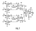
- Figure 7 shows a detection circuit for DTD4 for an apparatus according to the mvention for processing four detector signals as described above with reference to Figure 2.
- the four signals may be the signals C1, C2, C3 and C4 of the four detectors 31,32,33,34 as described with reference to Figure 3.
- the circuit shown in Figure 4 is a duplicate of inputs up to the low-pass filters, the signals C2 and C3 on the inputs 101, 111 being compared in the upper section and the signals C4 and C1 on the inputs 121,131 being compared in the lower section.
- the four inputs 101,102,103,104 are coupled to four digitizing sections each comprising a capacitor 102,112,122,132, a resistor 103,113,123,133 and a slicer 104,114,124,134 for generating four digitized signals S2, S3 and S4, S1.
- An upper delay unit 105 generates a delayed signal S2d based on the digitized signal S2, and a lower delay unit 125 generates a delayed signal S4d based on the digitized signal S4.
- the delayed signals S2d and S4d are compared with the digitized signals S2 and S3, and S4 and S1, respectively, by four comparators 106,116,126,136, which have outputs coupled to low-pass filters each having a series resistor 107,117,127,137 and a parallel capacitor 108,118,128,138.
- the four outputs of the low-pass filters are coupled to a single difference amplifier 115; the time difference signals based on S2 and S4 are coupled via difference input resistors 109,129 to the negative input of the difference amplifier 115 and the time difference signal baseds on S3 and S1 are coupled via difference input resistors 119,139 to the positive input of the difference amplifier 115 as indicated in the DTD4 formula.
- the tracking error signal TE is generated at the output of the difference amplifier 115 and coupled to the negative input via feedback resistor 110.
- the difference input resistors 109, 119, 129, 139 are much larger than the resistors 107,117,127,137 in the low-pass filters to prevent influencing of the low-pass filtering.
- the DTD4 circuit has the advantage that a reliable tracking error signal is generated in adverse scanning conditions.
Description
A problem of the apparatus is that the value of the tracking error signal is less reliable for short marks representing the information in high-density recording.
Claims (6)
- , Apparatus for scanning a record carrier (1) having a track comprising optically readable marks representing information, which apparatus comprises means (12,13,14) for scanning the record carrier via a radiation beam and tracking means (11) for controlling the position of the radiation beam in a direction transverse to the track direction on the basis of a tracking error signal, the tracking means comprising a detection unit (15) including a multitude of detectors (8) for receiving the radiation beam via the record carrier and an electronic circuit (10) for generating the tracking error signal in dependence on time differences between a first signal and a second signal, the first and the second signals being derived from output signals of the detectors, characterized in that the detection unit comprises digitizing means (44,54) for digitizing the first and second signal, delaying means (45) for generating a delayed signal based on the first or second digitized signal and comparing means (46,56) for comparing the delayed signal and the first and second digitized signals for generating the tracking error signal.
- Apparatus as claimed in Claim 1, in which the delayed signal is based on the signal, either the first or the second signal, that lags the other.
- Apparatus as claimed in Claim 1, in which the digitizing means comprise slicer means (44,54) and AC coupling means (42,52) for coupling the respective first or second signal to the slicer means for slicing the signal relative to a slicing level.
- Apparatus as claimed in Claim 1, in which the comparing means comprise means (46,56) for generating a first comparing signal in dependence on the difference between the delayed signal and the first digitized signal and a second comparing signal in dependence on the difference between the delayed signal and the second digitized signal, low-pass filtering means (47,48,57,58) for averaging the comparing signals and difference measuring means (55) coupled to the outputs of the low pass filtering means for generating the tracking error signal.
- Apparatus as claimed in Claim 1, characterized in that the detection unit comprises further digitizing means (124,134) for digitizing a third and a fourth signal derived from the outputs of the detectors, and second delaying means (125) for generating a second delayed signal based on the third and/or fourth digitized signal, and in that the comparing means comprise means (126,136) for comparing the second delayed signal with the third and/or fourth digitized signals.
- Detection unit for detecting a tracking error of a radiation beam scanning a record carrier having a track comprising optically readable marks representing information, the detection unit comprising a multitude of detectors (8) for receiving the radiation beam via the record carrier and an electronic circuit (10) for generating a tracking error signal in dependence on time differences between a first signal and a second signal, the first and second signals being derived from output signals of the detectors,
characterized in that the detection unit comprises digitizing means (44,54) for digitizing the first and the second signal, delaying means (45) for generating a delayed signal based on the first or the second digitized signal and comparing means (46,56) for comparing the delayed signal with the first and second digitized signals for generating the tracking error signal.
Priority Applications (1)
| Application Number | Priority Date | Filing Date | Title |
|---|---|---|---|
| EP98908253A EP0914652B1 (en) | 1997-04-25 | 1998-04-02 | Apparatus and detection unit for scanning an optically readable record carrier |
Applications Claiming Priority (4)
| Application Number | Priority Date | Filing Date | Title |
|---|---|---|---|
| EP97201244 | 1997-04-25 | ||
| EP97201244 | 1997-04-25 | ||
| PCT/IB1998/000481 WO1998049679A2 (en) | 1997-04-25 | 1998-04-02 | Apparatus and detection unit for scanning an optically readable record carrier |
| EP98908253A EP0914652B1 (en) | 1997-04-25 | 1998-04-02 | Apparatus and detection unit for scanning an optically readable record carrier |
Publications (2)
| Publication Number | Publication Date |
|---|---|
| EP0914652A2 EP0914652A2 (en) | 1999-05-12 |
| EP0914652B1 true EP0914652B1 (en) | 2005-07-06 |
Family
ID=8228260
Family Applications (1)
| Application Number | Title | Priority Date | Filing Date |
|---|---|---|---|
| EP98908253A Expired - Lifetime EP0914652B1 (en) | 1997-04-25 | 1998-04-02 | Apparatus and detection unit for scanning an optically readable record carrier |
Country Status (8)
| Country | Link |
|---|---|
| US (1) | US6137755A (en) |
| EP (1) | EP0914652B1 (en) |
| JP (1) | JP2000512791A (en) |
| CN (1) | CN1127724C (en) |
| DE (1) | DE69830774T2 (en) |
| MY (1) | MY120534A (en) |
| TW (1) | TW399202B (en) |
| WO (1) | WO1998049679A2 (en) |
Families Citing this family (19)
| Publication number | Priority date | Publication date | Assignee | Title |
|---|---|---|---|---|
| FR2792103B1 (en) * | 1999-03-16 | 2001-11-09 | St Microelectronics Sa | METHOD AND DEVICE FOR CONTROLLING AN OPTICAL BEAM INCIDENT ON A TRACK OF A MOBILE INFORMATION MEDIUM, IN PARTICULAR A DIGITAL DISK |
| JP2002298350A (en) * | 2001-03-28 | 2002-10-11 | Tdk Corp | Method, device, and medium for optical recording |
| JP3897671B2 (en) * | 2002-09-30 | 2007-03-28 | 三菱電機株式会社 | Status system signal processing circuit |
| CN1689081A (en) * | 2002-10-04 | 2005-10-26 | 皇家飞利浦电子股份有限公司 | High track density super resolution MO-ROM medium |
| TWI271726B (en) * | 2003-02-14 | 2007-01-21 | Ind Tech Res Inst | Circuit for tracking error signal detection on an optical storage medium |
| TWI248610B (en) * | 2003-04-07 | 2006-02-01 | Mediatek Inc | Method and related apparatus for deriving a tracking error signal |
| US7616536B2 (en) | 2003-05-21 | 2009-11-10 | Koninklijke Philips Electronics N.V. | Apparatus for radial tracking in an optical disc drive using tracking an error signal derived from wobble-induced signal components and/or data-induced signal components of a detector output |
| TWI295464B (en) * | 2003-08-22 | 2008-04-01 | Mediatek Inc | Control circuit for an optical pickup head in a disk drive |
| CN100365709C (en) * | 2003-09-09 | 2008-01-30 | 联发科技股份有限公司 | Control circuit for optical read-write head of CD-ROM drive |
| US7512043B2 (en) * | 2004-07-08 | 2009-03-31 | Realtek Semiconductor Corp. | Apparatus and method for generating a tracking error signal in an optical disc drive |
| TWI258740B (en) * | 2004-07-08 | 2006-07-21 | Realtek Semiconductor Corp | Apparatus and method for generating a tracking error signal in an optical disc drive |
| US7633842B2 (en) * | 2004-07-08 | 2009-12-15 | Realtek Semiconductor Corp. | Apparatus for generating tracking error signal in optical disc drive |
| US7583569B2 (en) * | 2004-07-08 | 2009-09-01 | Realtek Semiconductor Corp. | Apparatus and related method for generating a tracking error signal in an optical disc drive |
| JP4327693B2 (en) * | 2004-09-30 | 2009-09-09 | 株式会社東芝 | Optical disc apparatus and optical detection signal processing method |
| US20070047687A1 (en) * | 2005-08-25 | 2007-03-01 | Tse-Hsiang Hsu | Phase detector and related phase detecting method thereof |
| CN101072033B (en) * | 2006-05-11 | 2010-05-12 | 联咏科技股份有限公司 | Digital analogue converter and method |
| TWI345771B (en) | 2007-06-14 | 2011-07-21 | Sunplus Technology Co Ltd | Circuit for generating tracking error signal |
| EP2354840A1 (en) * | 2010-02-05 | 2011-08-10 | Siemens Aktiengesellschaft | An apparatus and a method for performing a difference measurement of an object image |
| JP2013073659A (en) * | 2011-09-29 | 2013-04-22 | Sanyo Electric Co Ltd | Optical pickup device |
Citations (1)
| Publication number | Priority date | Publication date | Assignee | Title |
|---|---|---|---|---|
| US4057833A (en) * | 1974-10-03 | 1977-11-08 | U.S. Philips Corporation | Centering detection system for an apparatus for playing optically readable record carriers |
Family Cites Families (10)
| Publication number | Priority date | Publication date | Assignee | Title |
|---|---|---|---|---|
| NL8303564A (en) * | 1983-10-17 | 1985-05-17 | Philips Nv | DEVICE FOR DISPLAYING INFORMATION FROM AN OPTICALLY READABLE RECORD CARRIER. |
| NL194811C (en) * | 1986-01-16 | 2003-03-04 | Mitsubishi Electric Corp | Servo circuit. |
| JPS6446237A (en) * | 1987-08-12 | 1989-02-20 | Canon Kk | Optical information recording and reproducing device |
| EP0343952A3 (en) * | 1988-05-26 | 1991-10-30 | Matsushita Electric Industrial Co., Ltd. | Focus error detection system for an optical recording/reproducing system |
| US5157645A (en) * | 1989-04-06 | 1992-10-20 | Kabushiki Kaisha Toshiba | Optical disk unit |
| JPH0423234A (en) * | 1990-05-18 | 1992-01-27 | Sony Corp | Tracking error signal generation device for optical device |
| JP2540224B2 (en) * | 1990-05-22 | 1996-10-02 | 松下電器産業株式会社 | Optical disk servo device |
| JP3166322B2 (en) * | 1992-06-15 | 2001-05-14 | ソニー株式会社 | Playback method and playback device |
| JP3426669B2 (en) * | 1993-11-22 | 2003-07-14 | 三洋電機株式会社 | Error signal generation circuit |
| JPH08263855A (en) * | 1995-03-23 | 1996-10-11 | Nec Corp | Optical head transfer controller |
-
1998
- 1998-04-02 CN CN98800802A patent/CN1127724C/en not_active Expired - Fee Related
- 1998-04-02 EP EP98908253A patent/EP0914652B1/en not_active Expired - Lifetime
- 1998-04-02 JP JP10529383A patent/JP2000512791A/en active Pending
- 1998-04-02 DE DE69830774T patent/DE69830774T2/en not_active Expired - Fee Related
- 1998-04-02 WO PCT/IB1998/000481 patent/WO1998049679A2/en active IP Right Grant
- 1998-04-20 US US09/062,943 patent/US6137755A/en not_active Expired - Fee Related
- 1998-04-22 MY MYPI98001803A patent/MY120534A/en unknown
- 1998-04-30 TW TW087106710A patent/TW399202B/en not_active IP Right Cessation
Patent Citations (1)
| Publication number | Priority date | Publication date | Assignee | Title |
|---|---|---|---|---|
| US4057833A (en) * | 1974-10-03 | 1977-11-08 | U.S. Philips Corporation | Centering detection system for an apparatus for playing optically readable record carriers |
Non-Patent Citations (1)
| Title |
|---|
| Härtel V. et al: *dRichtungsabhängige Strahlschranken*d, S.433-437 aus: *dDas Opto-Kochbuch*d; Texas Instruments Deutschland GmbH, 1975, ISBN 3-88078-000-5 * |
Also Published As
| Publication number | Publication date |
|---|---|
| US6137755A (en) | 2000-10-24 |
| MY120534A (en) | 2005-11-30 |
| JP2000512791A (en) | 2000-09-26 |
| CN1127724C (en) | 2003-11-12 |
| WO1998049679A2 (en) | 1998-11-05 |
| DE69830774D1 (en) | 2005-08-11 |
| DE69830774T2 (en) | 2006-05-18 |
| WO1998049679A3 (en) | 1999-02-04 |
| EP0914652A2 (en) | 1999-05-12 |
| CN1229504A (en) | 1999-09-22 |
| TW399202B (en) | 2000-07-21 |
Similar Documents
| Publication | Publication Date | Title |
|---|---|---|
| EP0914652B1 (en) | Apparatus and detection unit for scanning an optically readable record carrier | |
| US5631891A (en) | Disk reproducing circuit with automatic gain control | |
| EP0468613B1 (en) | Optical disk player | |
| EP0138273B1 (en) | Apparatus for reproducing information from an optically readable record carrier | |
| JPS63231733A (en) | Optical information reproduction system | |
| EP0363022B1 (en) | On/off-track signal in optical information recording and/or reproducing apparatus | |
| US5684771A (en) | Optical recording medium discriminating apparatus | |
| US20020041551A1 (en) | Optical disc playback apparatus and method of judging disc type | |
| CN101461001A (en) | Optimizing focus crosstalk cancelling | |
| JPH06333340A (en) | Information recording and reproducing device | |
| EP0800163B1 (en) | Apparatus and method for reproducing optical disk | |
| EP0491573B1 (en) | Optical disk drive | |
| US4974221A (en) | Method and apparatus for reproducing information by varying a sensitivity of a phase-locked loop in accordance with a detection state of a reproduced signal | |
| JPH0368456B2 (en) | ||
| JPH0778428A (en) | Access direction detecting circuit for disk device | |
| EP2093761A2 (en) | Optical disc apparatus | |
| JP2854131B2 (en) | Method for detecting that a light beam has left a data track and a detection circuit for detecting that a light beam has left a data track | |
| KR100538014B1 (en) | Devices and detectors for scanning optically readable recording media | |
| CN1272204A (en) | Optical recording medium | |
| EP0508522A2 (en) | Optical recording and/or reading apparatus | |
| US7065010B2 (en) | Method for tracking in an optical recording/reading apparatus, and corresponding apparatus | |
| JPS6052936A (en) | Generating circuit of tracking error signal for disk record | |
| JPS6040578A (en) | Disk record reproducer | |
| JP3652139B2 (en) | Tracking control circuit | |
| JPH08235763A (en) | Optical recording medium discriminating device |
Legal Events
| Date | Code | Title | Description |
|---|---|---|---|
| PUAI | Public reference made under article 153(3) epc to a published international application that has entered the european phase |
Free format text: ORIGINAL CODE: 0009012 |
|
| AK | Designated contracting states |
Kind code of ref document: A2 Designated state(s): DE FR GB |
|
| 17P | Request for examination filed |
Effective date: 19990125 |
|
| 17Q | First examination report despatched |
Effective date: 20030730 |
|
| GRAP | Despatch of communication of intention to grant a patent |
Free format text: ORIGINAL CODE: EPIDOSNIGR1 |
|
| GRAS | Grant fee paid |
Free format text: ORIGINAL CODE: EPIDOSNIGR3 |
|
| GRAA | (expected) grant |
Free format text: ORIGINAL CODE: 0009210 |
|
| AK | Designated contracting states |
Kind code of ref document: B1 Designated state(s): DE FR GB |
|
| REG | Reference to a national code |
Ref country code: GB Ref legal event code: FG4D |
|
| REF | Corresponds to: |
Ref document number: 69830774 Country of ref document: DE Date of ref document: 20050811 Kind code of ref document: P |
|
| ET | Fr: translation filed | ||
| PLBE | No opposition filed within time limit |
Free format text: ORIGINAL CODE: 0009261 |
|
| STAA | Information on the status of an ep patent application or granted ep patent |
Free format text: STATUS: NO OPPOSITION FILED WITHIN TIME LIMIT |
|
| 26N | No opposition filed |
Effective date: 20060407 |
|
| PGFP | Annual fee paid to national office [announced via postgrant information from national office to epo] |
Ref country code: DE Payment date: 20080617 Year of fee payment: 11 |
|
| PGFP | Annual fee paid to national office [announced via postgrant information from national office to epo] |
Ref country code: GB Payment date: 20080528 Year of fee payment: 11 |
|
| GBPC | Gb: european patent ceased through non-payment of renewal fee |
Effective date: 20090402 |
|
| REG | Reference to a national code |
Ref country code: FR Ref legal event code: ST Effective date: 20091231 |
|
| PG25 | Lapsed in a contracting state [announced via postgrant information from national office to epo] |
Ref country code: DE Free format text: LAPSE BECAUSE OF NON-PAYMENT OF DUE FEES Effective date: 20091103 |
|
| PG25 | Lapsed in a contracting state [announced via postgrant information from national office to epo] |
Ref country code: GB Free format text: LAPSE BECAUSE OF NON-PAYMENT OF DUE FEES Effective date: 20090402 Ref country code: FR Free format text: LAPSE BECAUSE OF NON-PAYMENT OF DUE FEES Effective date: 20091222 |
|
| PGFP | Annual fee paid to national office [announced via postgrant information from national office to epo] |
Ref country code: FR Payment date: 20080428 Year of fee payment: 11 |