EP0914015B1 - Optical add-drop multiplexer - Google Patents
Optical add-drop multiplexer Download PDFInfo
- Publication number
- EP0914015B1 EP0914015B1 EP98120406A EP98120406A EP0914015B1 EP 0914015 B1 EP0914015 B1 EP 0914015B1 EP 98120406 A EP98120406 A EP 98120406A EP 98120406 A EP98120406 A EP 98120406A EP 0914015 B1 EP0914015 B1 EP 0914015B1
- Authority
- EP
- European Patent Office
- Prior art keywords
- optical
- excitation light
- switch
- doped fiber
- transmission line
- Prior art date
- Legal status (The legal status is an assumption and is not a legal conclusion. Google has not performed a legal analysis and makes no representation as to the accuracy of the status listed.)
- Expired - Lifetime
Links
- 230000003287 optical effect Effects 0.000 title claims description 716
- 230000005284 excitation Effects 0.000 claims description 342
- 239000000835 fiber Substances 0.000 claims description 290
- 230000005540 biological transmission Effects 0.000 claims description 231
- 239000012535 impurity Substances 0.000 claims description 62
- 229910052691 Erbium Inorganic materials 0.000 description 185
- UYAHIZSMUZPPFV-UHFFFAOYSA-N erbium Chemical compound [Er] UYAHIZSMUZPPFV-UHFFFAOYSA-N 0.000 description 185
- 229920000642 polymer Polymers 0.000 description 36
- 238000003780 insertion Methods 0.000 description 34
- 230000037431 insertion Effects 0.000 description 34
- 229910052761 rare earth metal Inorganic materials 0.000 description 31
- 150000002910 rare earth metals Chemical class 0.000 description 31
- 238000010586 diagram Methods 0.000 description 14
- 238000010521 absorption reaction Methods 0.000 description 12
- 230000004048 modification Effects 0.000 description 8
- 238000012986 modification Methods 0.000 description 8
- 229910003327 LiNbO3 Inorganic materials 0.000 description 7
- 238000002347 injection Methods 0.000 description 7
- 239000007924 injection Substances 0.000 description 7
- 239000010453 quartz Substances 0.000 description 7
- 230000000630 rising effect Effects 0.000 description 7
- VYPSYNLAJGMNEJ-UHFFFAOYSA-N silicon dioxide Inorganic materials O=[Si]=O VYPSYNLAJGMNEJ-UHFFFAOYSA-N 0.000 description 7
- 229910052714 tellurium Inorganic materials 0.000 description 7
- PORWMNRCUJJQNO-UHFFFAOYSA-N tellurium atom Chemical compound [Te] PORWMNRCUJJQNO-UHFFFAOYSA-N 0.000 description 7
- 230000006866 deterioration Effects 0.000 description 6
- 230000008054 signal transmission Effects 0.000 description 4
- 230000009977 dual effect Effects 0.000 description 2
- 230000008878 coupling Effects 0.000 description 1
- 238000010168 coupling process Methods 0.000 description 1
- 238000005859 coupling reaction Methods 0.000 description 1
- 230000005855 radiation Effects 0.000 description 1
Images


Classifications
-
- H—ELECTRICITY
- H04—ELECTRIC COMMUNICATION TECHNIQUE
- H04Q—SELECTING
- H04Q11/00—Selecting arrangements for multiplex systems
- H04Q11/0001—Selecting arrangements for multiplex systems using optical switching
-
- H—ELECTRICITY
- H04—ELECTRIC COMMUNICATION TECHNIQUE
- H04J—MULTIPLEX COMMUNICATION
- H04J14/00—Optical multiplex systems
- H04J14/02—Wavelength-division multiplex systems
- H04J14/0201—Add-and-drop multiplexing
- H04J14/0202—Arrangements therefor
- H04J14/0204—Broadcast and select arrangements, e.g. with an optical splitter at the input before adding or dropping
-
- H—ELECTRICITY
- H04—ELECTRIC COMMUNICATION TECHNIQUE
- H04J—MULTIPLEX COMMUNICATION
- H04J14/00—Optical multiplex systems
- H04J14/02—Wavelength-division multiplex systems
- H04J14/0201—Add-and-drop multiplexing
- H04J14/0202—Arrangements therefor
- H04J14/0206—Express channels arrangements
-
- H—ELECTRICITY
- H04—ELECTRIC COMMUNICATION TECHNIQUE
- H04J—MULTIPLEX COMMUNICATION
- H04J14/00—Optical multiplex systems
- H04J14/02—Wavelength-division multiplex systems
- H04J14/0201—Add-and-drop multiplexing
- H04J14/0202—Arrangements therefor
- H04J14/021—Reconfigurable arrangements, e.g. reconfigurable optical add/drop multiplexers [ROADM] or tunable optical add/drop multiplexers [TOADM]
- H04J14/0212—Reconfigurable arrangements, e.g. reconfigurable optical add/drop multiplexers [ROADM] or tunable optical add/drop multiplexers [TOADM] using optical switches or wavelength selective switches [WSS]
-
- H—ELECTRICITY
- H04—ELECTRIC COMMUNICATION TECHNIQUE
- H04J—MULTIPLEX COMMUNICATION
- H04J14/00—Optical multiplex systems
- H04J14/02—Wavelength-division multiplex systems
- H04J14/0201—Add-and-drop multiplexing
- H04J14/0202—Arrangements therefor
- H04J14/0213—Groups of channels or wave bands arrangements
-
- H—ELECTRICITY
- H04—ELECTRIC COMMUNICATION TECHNIQUE
- H04J—MULTIPLEX COMMUNICATION
- H04J14/00—Optical multiplex systems
- H04J14/02—Wavelength-division multiplex systems
- H04J14/0221—Power control, e.g. to keep the total optical power constant
-
- H—ELECTRICITY
- H01—ELECTRIC ELEMENTS
- H01S—DEVICES USING THE PROCESS OF LIGHT AMPLIFICATION BY STIMULATED EMISSION OF RADIATION [LASER] TO AMPLIFY OR GENERATE LIGHT; DEVICES USING STIMULATED EMISSION OF ELECTROMAGNETIC RADIATION IN WAVE RANGES OTHER THAN OPTICAL
- H01S3/00—Lasers, i.e. devices using stimulated emission of electromagnetic radiation in the infrared, visible or ultraviolet wave range
- H01S3/05—Construction or shape of optical resonators; Accommodation of active medium therein; Shape of active medium
- H01S3/06—Construction or shape of active medium
- H01S3/063—Waveguide lasers, i.e. whereby the dimensions of the waveguide are of the order of the light wavelength
- H01S3/067—Fibre lasers
- H01S3/06754—Fibre amplifiers
- H01S3/06758—Tandem amplifiers
-
- H—ELECTRICITY
- H01—ELECTRIC ELEMENTS
- H01S—DEVICES USING THE PROCESS OF LIGHT AMPLIFICATION BY STIMULATED EMISSION OF RADIATION [LASER] TO AMPLIFY OR GENERATE LIGHT; DEVICES USING STIMULATED EMISSION OF ELECTROMAGNETIC RADIATION IN WAVE RANGES OTHER THAN OPTICAL
- H01S3/00—Lasers, i.e. devices using stimulated emission of electromagnetic radiation in the infrared, visible or ultraviolet wave range
- H01S3/09—Processes or apparatus for excitation, e.g. pumping
- H01S3/091—Processes or apparatus for excitation, e.g. pumping using optical pumping
- H01S3/094—Processes or apparatus for excitation, e.g. pumping using optical pumping by coherent light
- H01S3/094061—Shared pump, i.e. pump light of a single pump source is used to pump plural gain media in parallel
-
- H—ELECTRICITY
- H01—ELECTRIC ELEMENTS
- H01S—DEVICES USING THE PROCESS OF LIGHT AMPLIFICATION BY STIMULATED EMISSION OF RADIATION [LASER] TO AMPLIFY OR GENERATE LIGHT; DEVICES USING STIMULATED EMISSION OF ELECTROMAGNETIC RADIATION IN WAVE RANGES OTHER THAN OPTICAL
- H01S3/00—Lasers, i.e. devices using stimulated emission of electromagnetic radiation in the infrared, visible or ultraviolet wave range
- H01S3/14—Lasers, i.e. devices using stimulated emission of electromagnetic radiation in the infrared, visible or ultraviolet wave range characterised by the material used as the active medium
- H01S3/16—Solid materials
- H01S3/1601—Solid materials characterised by an active (lasing) ion
- H01S3/1603—Solid materials characterised by an active (lasing) ion rare earth
- H01S3/1608—Solid materials characterised by an active (lasing) ion rare earth erbium
Definitions
- the length of the rare earth doped fiber and a doping concentration thereof may be set in accordance with the required specifications of the optical switch.
- an optical output signal from the third optical transmission line 121 is free of any substantive noise and has an intensity of -60dBm or less.
- the excitation light switch 41 causes an insertion loss of 2dB and a crosstalk of 20dB which allow the optical switch to be free from any substantive insertion loss and a low or reduced crosstalk.
- the excitation light switch 41 is operated to switch to supply the excitation light to the second erbium doped fiber EDF12, then the second erbium doped fiber EDF12 is excited whereby the divided optical signal with the wavelength of 1550 nanometers is transmitted through the second erbium doped fiber EDF12 without any optical absorption.
- the optical output signal is then fed to the second optical filter 52 to remove or eliminate the noises from the optical output signal by the second optical filter 52 in order to avoid deterioration in signal-to-noise ratio due to provision of the excitation light switch 41. Therefore, the optical signal filtered in wavelength and having an intensity of 0dBm is outputted from the second optical transmission line 120.
- an optical output signal from the third optical transmission line 121 has an intensity of - 60dBm or less.
- the polymer optical switch 41 causes an insertion loss of 2dB and a crosstalk of 20dB which allow the optical switch to be free from any substantive insertion loss and a low or reduced crosstalk.
- an optical output signal from the third optical transmission line 121 has an intensity of -60dBm or less.
- the polymer optical switch 41 causes an insertion loss of 2dB and a crosstalk of 20dB which allow the optical switch to be free from any substantive insertion loss and a low or reduced crosstalk.
- FIG. 5 is a diagram illustrative a fifth optical switch having two inputs and two outputs, which is used in a novel optical add-drop multiplexer.
- a structural difference of the sixth novel optical switch from the fourth optical switch is in providing a single or common excitation light source to a pair of modified first optical switches excluding individual excitation light sources described in the first embodiment.
- the fifth optical switch comprises a pair of the first novel optical switches described in the first embodiment.
- the two first novel optical switches are connected to each other through a first optical transmission line 110 as a common line.
- the two first novel optical switches are connected are also connected to the single and common excitation light source 31 to reduce the number of the required excitation light source.
- the fourth optical transmission line 1 comprises a fourth input side optical transmission line 214 and a fourth output side optical transmission line 224, wherein the fourth input side optical transmission line 214 is connected through a fourth erbium doped fiber 14EDF to the fourth input side optical transmission line 214.
- a fourth optical coupler 24 is provided on the fourth input side optical transmission line 214.
- the fourth optical coupler 24 is connected to a fourth output of the excitation light switch 41.
- a fourth optical signal is transmitted on the fourth input side optical transmission line 214 through the fourth erbium doped fiber 14EDF to the fourth input side optical transmission line 214.
Description
- The present invention relates to an optical add-drop multiplexer.
- From US-A-5 121 450 a fiber optical Y-junction is known, which comprises multiple optical inputs, multiple optical outputs and fiber optic amplifier modules. By coupling the fiber optic amplifiers with fiber couplers an all-fiber optical switch offering little radiation loss, but no add-drop multiplexer, can be formed.
- Accordingly, it is an object of the present invention to provide a novel optical add-drop multiplexer.
- The first present invention provides an optical add-drop multiplexer comprising at least a single set of the following elements. An input side optical transmission line is provided for transmitting a first optical signal. An input side optical coupler is provided on the first optical transmission line for dividing the first optical signal into first and second divided optical signals. First and second optical transmission lines are provided which are connected with the input side optical coupler for transmissions of the first and second divided optical signals respectively. The first and second optical transmission lines have first and second impurity doped fibers. An optical receiver is provided which is connected through the first optical transmission line to the first impurity doped fiber for receiving the first divided optical signal only when the first impurity doped fiber is excited. An optical transmitter is provided which is connected through the second optical transmission line to the second impurity doped fiber for transmitting a second optical signal through the second impurity doped fiber to the input side optical transmission line for output of the second optical signal only when the second impurity doped fiber is excited. At least an excitation light source is provided for emitting an excitation light. An excitation light switch is provided which is connected to the excitation light source and also connected to the first and second optical transmission lines for selective switching operations to supply the excitation light to any one of the first and second optical transmission lines to feed the excitation light to selected one of the first and second impurity doped fibers, thereby causing an excitation of the selected one of the first and second impurity doped fibers, whilst unselected one of the first and second impurity doped fibers is unexcited.
- It is preferable that the optical add-drop multiplexer comprises a plurality of the optical add-drop multiplexers, and further comprising an optical device having at least any one of multiplexing function and demultiplexing function so that the optical add-drop multiplexers are operable to different wavelength optical signals.
- The above and other objects, features and advantages of the present invention will be apparent from the following descriptions.
- Preferred embodiments according to the present invention will be described in detail with reference to the accompanying drawings.
- FIG. 1 is a diagram illustrative of a first optical switch having a single input and two outputs in a first embodiment of a not shown novel optical add-drop multiplexer using said first optical switch in accordance with the present invention.
- FIG. 2 is a diagram illustrative of a second optical switch having a single input and two outputs in a second embodiment of a not shown novel optical add-drop multiplexer using said second optical switch in accordance with the present invention.
- FIG. 3 is a diagram illustrative of a third optical switch having a single input and two outputs in a third embodiment of a not shown novel optical add-drop multiplexer using said third optical switch in accordance with the present invention.
- FIG. 4 is a diagram illustrative of a fourth optical switch having two inputs and two outputs in a fourth embodiment of a not shown novel optical add-drop multiplexer using said fourth optical switch in accordance with the present invention.
- FIG. 5 is a diagram illustrative of a fifth optical switch having two inputs and two outputs in a fifth embodiment of a not shown novel optical add-drop multiplexer using said fifth optical switch in accordance with the present invention.
- FIG. 6 is a diagram illustrative of a sixth optical switch having four separate optical transmission lines for separately switching optical signal transmissions on the four separate optical transmission lines in a sixth embodiment of a not shown novel optical add-drop multiplexer using said sixth optical switch in accordance with the present invention.
- FIG. 7 is a diagram illustrative of a seventh optical switch having four separate optical transmission lines for separately switching optical signal transmissions on the four separate optical transmission lines in a seventh embodiment of a not shown novel optical add-drop multiplexer using said seventh optical switch in accordance with the present invention.
- The present invention provides an optical add-drop multiplexer comprising at least a single set of the following elements. An input side optical transmission line is provided for transmitting a first optical signal. An input side optical coupler is provided on the first optical transmission line for dividing the first optical signal into first and second divided optical signals. First and second optical transmission lines are provided which are connected with the input side optical coupler for transmissions of the first and second divided optical signals respectively. The first and second optical transmission lines have first and second impurity doped fibers. An optical receiver is provided which is connected through the first optical transmission line to the first impurity doped fiber for receiving the first divided optical signal only when the first impurity doped fiber is excited. An optical transmitter is provided which is connected through the second optical transmission line to the second impurity doped fiber for transmitting a second optical signal through the second impurity doped fiber to the input side optical transmission line for output of the second optical signal only when the second impurity doped fiber is excited. At least an excitation light source is provided for emitting an excitation light. An excitation light switch is provided which is connected to the excitation light source and also connected to the first and second optical transmission lines for selective switching operations to supply the excitation light to any one of the first and second optical transmission lines to feed the excitation light to selected one of the first and second impurity doped fibers, thereby causing an excitation of the selected one of the first and second impurity doped fibers, whilst unselected one of the first and second impurity doped fibers is unexcited.
- It is preferable that the optical add-drop multiplexer comprises a plurality of the optical add-drop multiplexers, and further comprising an optical device having at least any one of multiplexing function and demultiplexing function so that the optical add-drop multiplexers are operable to different wavelength optical signals.
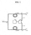
- A first embodiment according to the present invention will be described in details with reference to FIG. 1 which is a diagram illustrative of a first optical switch having a single input and two outputs, used in a novel optical add-drop multiplexer. The optical switch has an
input side coupler 21 which is connected to a firstoptical transmission line 110 on which an optical input signal is transmitted and then inputted into the optical switch. The optical input signal has a wavelength of 1550 nanometers and an intensity of 0dBm. The optical input signal is divided by theinput side coupler 21 into two parts. The optical switch has second and thirdoptical transmission lines input side coupler 21. The two divided optical signals are then transmitted through the second and thirdoptical transmission lines optical transmission line 120 is connected to a firstoutput side coupler 22. The thirdoptical transmission line 121 is connected to a second output sideoptical coupler 23. A first erbium doped fiber EDF11 is provided on the secondoptical transmission line 120 between theinput side coupler 21 and the firstoutput side coupler 22. A second erbium doped fiber EDF12 is provided on the thirdoptical transmission line 120 between theinput side coupler 21 and the secondoutput side coupler 23. The first and second erbium doped fibers EDF11 and EDF12 have a length of 50 meters. The first and second erbium doped fibers EDF11 and EDF12 may be replaced by rare earth doped fibers. The two divided optical signals are transmitted through the first and second erbium doped fibers EDF11 and EDF12 respectively. The optical switch further has anexcitation light switch 41 which is connected through a first excitationlight transmission line 111 to the firstoutput side coupler 22 as well as which is connected through a second excitationlight transmission line 112 to the secondoutput side coupler 23. The optical switch further has an excitation light source 31 which is connected to theexcitation light switch 41. The excitation light source 31 emits an excitation light with a wavelength of 1480 nanometers. Theexcitation light switch 41 is operated to switch the excitation light to any one of the first and second excitationlight transmission lines - If the
excitation light switch 41 is operated to switch to supply the excitation light to the first erbium doped fiber EDF11, then the first erbium doped fiber EDF11 is excited whereby the divided optical signal with the wavelength of 1550 nanometers is transmitted through the first erbium doped fiber EDF11 without any optical absorption and then the optical signal with an intensity of 0dBm is outputted from the secondoptical transmission line 120. Accurately, the majority part of the excitation light emitted from the excitation light source 31 is switched by theexcitation light switch 41 to be fed through the first excitationlight transmission line 111 and the first output sideoptical coupler 22 to the first erbium doped fiber EDF11. On the other hand, the minority part of the excitation light emitted from the excitation light source 31 might be leaked through theexcitation light switch 41 whereby a leaked excitation light is then fed through the second output sideoptical coupler 23 to the second erbium doped fiber EDF12. However, the leaked excitation light is incapable of exciting the second erbium doped fiber EDF12, for which reason the divided optical signal with the wavelength of 1550 nanometers is absorbed into the second erbium doped fiber EDF12. As a result, an optical output signal from the thirdoptical transmission line 121 has an intensity of -60dBm or less. Theexcitation light switch 41 causes an insertion loss of 2dB and a crosstalk of 20dB which allow the optical switch to be free from any substantive insertion loss and a low or reduced crosstalk. - If the
excitation light switch 41 is operated to switch to supply the excitation light to the second erbium doped fiber EDF12, then the second erbium doped fiber EDF12 is excited whereby the divided optical signal with the wavelength of 1550 nanometers is transmitted through the second erbium doped fiber EDF12 without any optical absorption and then the optical signal with an intensity of 0dBm is outputted from the thirdoptical transmission line 121. Accurately, the majority part of the excitation light emitted from the excitation light source 31 is switched by theexcitation light switch 41 to be fed through the second excitationlight transmission line 112 and the second output sideoptical coupler 23 to the second erbium doped fiber EDF12. On the other hand, the minority part of the excitation light emitted from the excitation light source 31 might be leaked through theexcitation light switch 41 whereby a leaked excitation light is then fed through the first output sideoptical coupler 22 to the first erbium doped fiber EDF11. However, the leaked excitation light is incapable of exciting the first erbium doped fiber EDF11, for which reason the divided optical signal with the wavelength of 1550 nanometers is absorbed into the first erbium doped fiber EDF11. As a result, an optical output signal from the thirdoptical transmission line 121 has an intensity of -60dBm or less. Theexcitation light switch 41 causes an insertion loss of 2dB and a crosstalk of 20dB which allow the optical switch to be free from any substantive insertion loss and a low or reduced crosstalk. - As a modification to the above first embodiment, the above
excitation light switch 41 may be replaced by a polymer optical switch. - If the polymer
optical switch 41 is operated to switch to supply the excitation light to the first erbium doped fiber EDF11, then the first erbium doped fiber EDF11 is excited whereby the divided optical signal with the wavelength of 1550 nanometers is transmitted through the first erbium doped fiber EDF11 without any optical absorption and then the optical signal with an intensity of 0dBm is outputted from the secondoptical transmission line 120. Accurately, the majority part of the excitation light emitted from the excitation light source 31 is switched by the polymeroptical switch 41 to be fed through the first excitationlight transmission line 111 and the first output sideoptical coupler 22 to the first erbium doped fiber EDF11. On the other hand, the minority part of the excitation light emitted from the excitation light source 31 might be leaked through the polymeroptical switch 41 whereby a leaked excitation light is then fed through the second output sideoptical coupler 23 to the second erbium doped fiber EDF12. However, the leaked excitation light is incapable of exciting the second erbium doped fiber EDF12, for which reason the divided optical signal with the wavelength of 1550 nanometers is absorbed into the second erbium doped fiber EDF12. As a result, an optical output signal from the thirdoptical transmission line 121 has an intensity of - 60dBm or less. The polymeroptical switch 41 causes an insertion loss of 2dB and a crosstalk of 20dB which allow the optical switch to be free from any substantive insertion loss and a low or reduced crosstalk. - If the polymer
optical switch 41 is operated to switch to supply the excitation light to the second erbium doped fiber EDF12, then the second erbium doped fiber EDF12 is excited whereby the divided optical signal with the wavelength of 1550 nanometers is transmitted through the second erbium doped fiber EDF12 without any optical absorption and then the optical signal with an intensity of 0dBm is outputted from the thirdoptical transmission line 121. Accurately, the majority part of the excitation light emitted from the excitation light source 31 is switched by the polymeroptical switch 41 to be fed through the second excitationlight transmission line 112 and the second output sideoptical coupler 23 to the second erbium doped fiber EDF12. On the other hand, the minority part of the excitation light emitted from the excitation light source 31 might be leaked through the polymeroptical switch 41 whereby a leaked excitation light is then fed through the first output sideoptical coupler 22 to the first erbium doped fiber EDF11. However, the leaked excitation light is incapable of exciting the first erbium doped fiber EDF11, for which reason the divided optical signal with the wavelength of 1550 nanometers is absorbed into the first erbium doped fiber EDF11. As a result, an optical output signal from the thirdoptical transmission line 121 has an intensity of -60dBm or less. The polymeroptical switch 41 causes an insertion loss of 2dB and a crosstalk of 20dB which allow the optical switch to be free from any substantive insertion loss and a low or reduced crosstalk. - As a further modification to the above first embodiment, the excitation light has a wavelength of 980 nanometers in order to shorten the wavelength for a remarkable reduction in noise factor of the optical output signal. In this case, the optical switch is also free from any substantive insertion loss and a low or reduced crosstalk.
- In the above embodiment, the number of the wavelength multiplexing on each optical transmission line is one. Notwithstanding, 8, 16, 32, 64-wavelength multiplexing are available, wherein the batch-switching operation to the plural number wavelength multiplexing is carried out.
- It is also possible to set the wavelength of the optical input signal at not only 1550 nanometers but also other wavelengths, for example, 1330 nanometers.
- It is also possible to set the wavelength of the excitation light at not only 1480 nanometers or 980 nanometers but also other wavelengths provided that such wavelength is capable of exciting the impurity doped fiber. It is preferable to set the wavelength of the excitation light in consideration of both the wavelength of the optical input signal and the kind of the impurity doped fiber.
- The above excitation light switch may also be replaced by an acousto-optical switch, or a quartz-based switch.
- It is further possible to control an intensity of the optical output signal by controlling an optical power of the excitation light to be fed to the impurity doped fiber. It is possible to control the optical power of the excitation light to be fed to the impurity doped fiber by controlling an injection current to the excitation light source or by use of variable or fixed attenuator.
- It is furthermore possible to replace the erbium doped fiber by rare earth doped fiber such as tellurium doped fiber. The length of the rare earth doped fiber and a doping concentration thereof may be set in accordance with the required specifications of the optical switch.
- It is moreover possible to input the excitation light into the rare earth doped fiber in either directions or in both directions.
- It is still more possible to conduct a polarization-multiplexing to different excitation lights emitted separately from plural different excitation light sources in order to input the polarization-multiplexed excitation light into the rare earth doped fiber to obtain a high gain.
- It is yet more possible to set freely a ratio of optical division at the optical coupler in accordance with the various design choices.
- The provisions of the smaller number of the excitation light source and the single excitation light switch permit ON-OFF switching operations of the plural gate switches by a simple structure. The above switch exhibits such a gain property as a sharp rising, for which reason there is substantially no influence due to a leaked light from the excitation light switch. This makes the switch available to switches having relatively large crosstalk levels such as a polymer type switch or LiNbO3 switch, thereby realizing a low crosstalk and low insertion loss optical switch. In addition, the use of the impurity doped fiber serving as an optical power amplifier can obtain a gain as the optical switch.
- A second embodiment according to the present invention will be described in detail with reference to FIG. 2 which is a diagram illustrative of a second optical switch having a single input and two outputs which is used in a novel optical add-drop multiplexer. A structural difference of the second novel optical switch from the first novel optical switch is only in further providing first and second optical filters on two output sides in order to eliminate or remove amplified noises from the optical output signals.
- The optical switch has an
input side coupler 21 which is connected to a firstoptical transmission line 110 on which an optical input signal is transmitted and then inputted into the optical switch. The optical input signal has a wavelength of 1550 nanometers and an intensity of 0dBm. The optical input signal is divided by theinput side coupler 21 into two parts. The optical switch has second and thirdoptical transmission lines input side coupler 21. The two divided optical signals are then transmitted through the second and thirdoptical transmission lines optical transmission line 120 is connected to a firstoutput side coupler 22. The thirdoptical transmission line 121 is connected to a second output sideoptical coupler 23. A first erbium doped fiber EDF11 is provided on the secondoptical transmission line 120 between theinput side coupler 21 and the firstoutput side coupler 22. A second erbium doped fiber EDF12 is provided on the thirdoptical transmission line 120 between theinput side coupler 21 and the secondoutput side coupler 23. The first and second erbium doped fibers EDF11 and EDF12 have a length of 50 meters. The first and second erbium doped fibers EDF11 and EDF12 may be replaced by rare earth doped fibers. The two divided optical signals are transmitted through the first and second erbium doped fibers EDF11 and EDF12 respectively. The optical switch further has anexcitation light switch 41 which is connected through a first excitationlight transmission line 111 to the firstoutput side coupler 22 as well as which is connected through a second excitationlight transmission line 112 to the secondoutput side coupler 23. The optical switch further has an excitation light source 31 which is connected to theexcitation light switch 41. The excitation light source 31 emits an excitation light with a wavelength of 1480 nanometers. Theexcitation light switch 41 is operated to switch the excitation light to any one of the first and second excitationlight transmission lines - Further, in this second embodiment, a first optical filter 51 is provided on the second
optical transmission line 120 and positioned closer to the output side than the first output sideoptical coupler 22. If the first erbium doped fiber EDF11 is excited, then this first erbium doped fiber EDF11 also serves as an optical power amplifier which, however, amplifies not only the divided optical signal from the firstoptical transmission line 110 but also noises included in the optical signals, for which reason it is preferable to remove or eliminate the noises from the optical output signal by the first optical filter 51 in order to avoid deterioration in signal-to-noise ratio due to provision of theexcitation light switch 41. Similarly, a second optical filter 52 is provided on the thirdoptical transmission line 121 and positioned closer to the output side than the second output sideoptical coupler 23. If the second erbium doped fiber EDF12 is excited, then this second erbium doped fiber EDF12 also serves as an optical power amplifier which, however, amplifies not only the divided optical signal from the firstoptical transmission line 110 but also noises included in the optical signals, for which reason it is preferable to remove or eliminate the noises from the optical output signal by the second optical filter 52 in order to avoid deterioration in signal-to-noise ratio due to provision of theexcitation light switch 41. - If the
excitation light switch 41 is operated to switch to supply the excitation light to the first erbium doped fiber EDF11, then the first erbium doped fiber EDF11 is excited whereby the divided optical signal with the wavelength of 1550 nanometers is transmitted through the first erbium doped fiber EDF11 without any optical absorption. The optical output signal is then fed to the first optical filter 51 to remove or eliminate the noises from the optical output signal by the first optical filter 51 in order to avoid deterioration in signal-to-noise ratio due to provision of theexcitation light switch 41. Therefore, the optical signal filtered in wavelength and having an intensity of 0dBm is outputted from the secondoptical transmission line 120. Accurately, the majority part of the excitation light emitted from the excitation light source 31 is switched by theexcitation light switch 41 to be fed through the first excitationlight transmission line 111 and the first output sideoptical coupler 22 to the first erbium doped fiber EDF11. On the other hand, the minority part of the excitation light emitted from the excitation light source 31 might be leaked through theexcitation light switch 41 whereby a leaked excitation light is then fed through the second output sideoptical coupler 23 to the second erbium doped fiber EDF12. However, the leaked excitation light is incapable of exciting the second erbium doped fiber EDF12, for which reason the divided optical signal with the wavelength of 1550 nanometers is absorbed into the second erbium doped fiber EDF12. As a result, an optical output signal from the thirdoptical transmission line 121 is free of any substantive noise and has an intensity of -60dBm or less. Theexcitation light switch 41 causes an insertion loss of 2dB and a crosstalk of 20dB which allow the optical switch to be free from any substantive insertion loss and a low or reduced crosstalk. - If the
excitation light switch 41 is operated to switch to supply the excitation light to the second erbium doped fiber EDF12, then the second erbium doped fiber EDF12 is excited whereby the divided optical signal with the wavelength of 1550 nanometers is transmitted through the second erbium doped fiber EDF12 without any optical absorption. The optical output signal is then fed to the second optical filter 52 to remove or eliminate the noises from the optical output signal by the second optical filter 52 in order to avoid deterioration in signal-to-noise ratio due to provision of theexcitation light switch 41. Therefore, the optical signal filtered in wavelength and having an intensity of 0dBm is outputted from the secondoptical transmission line 120. Accurately, the majority part of the excitation light emitted from the excitation light source 31 is switched by theexcitation light switch 41 to be fed through the second excitationlight transmission line 112 and the second output sideoptical coupler 23 to the second erbium doped fiber EDF12. On the other hand, the minority part of the excitation light emitted from the excitation light source 31 might be leaked through theexcitation light switch 41 whereby a leaked excitation light is then fed through the first output sideoptical coupler 22 to the first erbium doped fiber EDF11. However, the leaked excitation light is incapable of exciting the first erbium doped fiber EDF11, for which reason the divided optical signal with the wavelength of 1550 nanometers is absorbed into the first erbium doped fiber EDF11. As a result, an optical output signal from the thirdoptical transmission line 121 is free of any substantive noise and has an intensity of -60dBm or less. Theexcitation light switch 41 causes an insertion loss of 2dB and a crosstalk of 20dB which allow the optical switch to be free from any substantive insertion loss and a low or reduced crosstalk. - As a modification to the above second embodiment, the above
excitation light switch 41 may be replaced by a polymer optical switch similarly to the first embodiment. - If the polymer
optical switch 41 is operated to switch to supply the excitation light to the first erbium doped fiber EDF11, then the first erbium doped fiber EDF11 is excited whereby the divided optical signal with the wavelength of 1550 nanometers is transmitted through the first erbium doped fiber EDF11 without any optical absorption. The optical output signal is then fed to the first optical filter 51 to remove or eliminate the noises from the optical output signal by the first optical filter 51 in order to avoid deterioration in signal-to-noise ratio due to provision of the polymeroptical switch 41. Therefore, the optical signal filtered in wavelength and having an intensity of 0dBm is outputted from the secondoptical transmission line 120. Accurately, the majority part of the excitation light emitted from the excitation light source 31 is switched by the polymeroptical switch 41 to be fed through the first excitationlight transmission line 111 and the first output sideoptical coupler 22 to the first erbium doped fiber EDF11. On the other hand, the minority part of the excitation light emitted from the excitation light source 31 might be leaked through the polymeroptical switch 41 whereby a leaked excitation light is then fed through the second output sideoptical coupler 23 to the second erbium doped fiber EDF12. However, the leaked excitation light is incapable of exciting the second erbium doped fiber EDF12, for which reason the divided optical signal with the wavelength of 1550 nanometers is absorbed into the second erbium doped fiber EDF12. As a result, an optical output signal from the thirdoptical transmission line 121 is free of any substantive noise and has an intensity of -60dBm or less. The polymeroptical switch 41 causes an insertion loss of 2dB and a crosstalk of 20dB which allow the optical switch to be free from any substantive insertion loss and a low or reduced crosstalk. - If the polymer
optical switch 41 is operated to switch to supply the excitation light to the second erbium doped fiber EDF12, then the second erbium doped fiber EDF12 is excited whereby the divided optical signal with the wavelength of 1550 nanometers is transmitted through the second erbium doped fiber EDF12 without any optical absorption. The optical output signal is then fed to the second optical filter 52 to remove or eliminate the noises from the optical output signal by the second optical filter 52 in order to avoid deterioration in signal-to-noise ratio due to provision of the polymeroptical switch 41. Therefore, the optical signal filtered in wavelength and having an intensity of 0dBm is outputted from the secondoptical transmission line 120. Accurately, the majority part of the excitation light emitted from the excitation light source 31 is switched by the polymeroptical switch 41 to be fed through the second excitationlight transmission line 112 and the second output sideoptical coupler 23 to the second erbium doped fiber EDF12. On the other hand, the minority part of the excitation light emitted from the excitation light source 31 might be leaked through the polymeroptical switch 41 whereby a leaked excitation light is then fed through the first output sideoptical coupler 22 to the first erbium doped fiber EDF11. However, the leaked excitation light is incapable of exciting the first erbium doped fiber EDF11, for which reason the divided optical signal with the wavelength of 1550 nanometers is absorbed into the first erbium doped fiber EDF11. As a result, an optical output signal from the thirdoptical transmission line 121 is free of any substantive noise and has an intensity of -60dBm or less. The polymeroptical switch 41 causes an insertion loss of 2dB and a crosstalk of 20dB which allow the optical switch to be free from any substantive insertion loss and a low or reduced crosstalk. - As a further modification to the above second embodiment, the excitation light has a wavelength of 980 nanometers in order to shorten the wavelength for a remarkable reduction in noise factor of the optical output signal. In this case, the optical switch is also free from any substantive insertion loss and a low or reduced crosstalk.
- In the above embodiment, the number of the wavelength multiplexing on each optical transmission line is one. Notwithstanding, 8, 16, 32, 64-wavelength multiplexing are available, wherein the batch-switching operation to the plural number wavelength multiplexing is carried out.
- It is also possible to set the wavelength of the optical input signal at not only 1550 nanometers but also other wavelengths, for example, 1330 nanometers.
- It is also possible to set the wavelength of the excitation light at not only 1480 nanometers or 980 nanometers but also other wavelengths provided that such wavelength is capable of exciting the impurity doped fiber. It is preferable to set the wavelength of the excitation light in consideration of both the wavelength of the optical input signal and the kind of the impurity doped fiber.
- The above excitation light switch may also be replaced by an acousto-optical switch, or a quartz-based switch.
- It is further possible to control an intensity of the optical output signal by controlling an optical power of the excitation light to be fed to the impurity doped fiber. It is possible to control the optical power of the excitation light to be fed to the impurity doped fiber by controlling an injection current to the excitation light source or by use of variable or fixed attenuator.
- It is furthermore possible to replace the erbium doped fiber by rare earth doped fiber such as tellurium doped fiber. The length of the rare earth doped fiber and a doping concentration thereof may be set in accordance with the required specifications of the optical switch.
- It is moreover possible to input the excitation light into the rare earth doped fiber in either directions or in both directions.
- It is still more possible to conduct a polarization-multiplexing to different excitation lights emitted separately from plural different excitation light sources in order to input the polarization-multiplexed excitation light into the rare earth doped fiber to obtain a high gain.
- It is yet more possible to set freely a ratio of optical division at the optical coupler in accordance with the various design choices.
- It is still further possible to freely set the transmission-band width in accordance with the number of the optical signals to be transmitted through the optical switch.
- It is yet further possible to provide optical filters and optical isolators since the excitation light and returned light provide no influence to input and output sides of the optical switch.
- The provisions of the smaller number of the excitation light source and the single excitation light switch permit ON-OFF switching operations of the plural gate switches by a simple structure. The above switch exhibits such a gain property as a sharp rising, for which reason there is substantially no influence due to a leaked light from the excitation light switch. This makes the switch available to switches having relatively large crosstalk levels such as a polymer type switch or LiNbO3 switch, thereby realizing a low crosstalk and low insertion loss optical switch. In addition, the use of the impurity doped fiber serving as an optical power amplifier can obtain a gain as the optical switch.
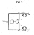
- A third embodiment according to the present invention will be described in detail with reference to FIG. 3 which is a diagram illustrative a third optical switch having a single input and two outputs which is used in a novel optical add-drop multiplexer. A structural difference of the third novel optical switch from the first novel optical switch is in positions of first and second erbium doped fibers so that first and second erbium doped fibers receive an excitation light in the same direction as receipt of the optical signals, whilst in the first embodiment the first and second erbium doped fibers receive the excitation light in the opposite direction to the receipt of the optical signals.
- The optical switch has an
input side coupler 21 which is connected to a firstoptical transmission line 110 on which an optical input signal is transmitted and then inputted into the optical switch. The optical input signal has a wavelength of 1550 nanometers and an intensity of 0dBm. The optical input signal is divided by theinput side coupler 21 into two parts. The optical switch has second and thirdoptical transmission lines input side coupler 21. The two divided optical signals are then transmitted through the second and thirdoptical transmission lines optical transmission line 120 is connected to a firstoutput side coupler 22. The thirdoptical transmission line 121 is connected to a second output sideoptical coupler 23. A first erbium doped fiber EDF11 is provided on the secondoptical transmission line 120 and positioned between the firstoutput side coupler 22 and the output terminal of the secondoptical transmission line 120. A second erbium doped fiber EDF12 is provided on the thirdoptical transmission line 120 and positioned between the secondoutput side coupler 23 and the output terminal of the thirdoptical transmission line 121. The first and second erbium doped fibers EDF11 and EDF12 have a length of 50 meters. The first and second erbium doped fibers EDF11 and EDF12 may be replaced by rare earth doped fibers. The two divided optical signals are transmitted through the first and second erbium doped fibers EDF11 and EDF12 respectively. The optical switch further ahs anexcitation light switch 41 which is connected through a first excitationlight transmission line 111 to the firstoutput side coupler 22 as well as which is connected through a second excitationlight transmission line 112 to the secondoutput side coupler 23. The optical switch further has an excitation light source 31 which is connected to theexcitation light switch 41. The excitation light source 31 emits an excitation light with a wavelength of 1480 nanometers. Theexcitation light switch 41 is operated to switch the excitation light to any one of the first and second excitationlight transmission lines - If the
excitation light switch 41 is operated to switch to supply the excitation light to the first erbium doped fiber EDF11 so that the first and second erbium doped fiber EDF11 receives the excitation light in the same direction as receipt of the optical signal, then the first erbium doped fiber EDF11 is excited whereby the divided optical signal with the wavelength of 1550 nanometers is transmitted through the first erbium doped fiber EDF11 without any optical absorption and then the optical signal with an intensity of 0dBm is outputted from the secondoptical transmission line 120. Accurately, the majority part of the excitation light emitted from the excitation light source 31 is switched by theexcitation light switch 41 to be fed through the first excitationlight transmission line 111 and the first output sideoptical coupler 22 to the first erbium doped fiber EDF11. On the other hand, the minority part of the excitation light emitted from the excitation light source 31 might be leaked through theexcitation light switch 41 whereby a leaked excitation light is then fed through the second output sideoptical coupler 23 to the second erbium doped fiber EDF12. However, the leaked excitation light is incapable of exciting the second erbium doped fiber EDF12, for which reason the divided optical signal with the wavelength of 1550 nanometers is absorbed into the second erbium doped fiber EDF12. As a result, an optical output signal from the thirdoptical transmission line 121 has an intensity of - 60dBm or less. Theexcitation light switch 41 causes an insertion loss of 2dB and a crosstalk of 20dB which allow the optical switch to be free from any substantive insertion loss and a low or reduced crosstalk. - If the
excitation light switch 41 is operated to switch to supply the excitation light to the second erbium doped fiber EDF12 so that the second erbium doped fiber EDF12 receives the excitation light in the same direction as receipt of the optical signal, then the second erbium doped fiber EDF12 is excited whereby the divided optical signal with the wavelength of 1550 nanometers is transmitted through the second erbium doped fiber EDF12 without any optical absorption and then the optical signal with an intensity of 0dBm is outputted from the thirdoptical transmission line 121. Accurately, the majority part of the excitation light emitted from the excitation light source 31 is switched by theexcitation light switch 41 to be fed through the second excitationlight transmission line 112 and the second output sideoptical coupler 23 to the second erbium doped fiber EDF12. On the other hand, the minority part of the excitation light emitted from the excitation light source 31 might be leaked through theexcitation light switch 41 whereby a leaked excitation light is then fed through the first output sideoptical coupler 22 to the first erbium doped fiber EDF11. However, the leaked excitation light is incapable of exciting the first erbium doped fiber EDF11, for which reason the divided optical signal with the wavelength of 1550 nanometers is absorbed into the first erbium doped fiber EDF11. As a result, an optical output signal from the thirdoptical transmission line 121 has an intensity of -60dBm or less. Theexcitation light switch 41 causes an insertion loss of 2dB and a crosstalk of 20dB which allow the optical switch to be free from any substantive insertion loss and a low or reduced crosstalk. - As a modification to the above first embodiment, the above
excitation light switch 41 may be replaced by a polymer optical switch. - If the polymer
optical switch 41 is operated to switch to supply the excitation light to the first erbium doped fiber EDF11 so that the first and second erbium doped fiber EDF11 receives the excitation light in the same direction as receipt of the optical signal, then the first erbium doped fiber EDF11 is excited whereby the divided optical signal with the wavelength of 1550 nanometers is transmitted through the first erbium doped fiber EDF11 without any optical absorption and then the optical signal with an intensity of 0dBm is outputted from the secondoptical transmission line 120. Accurately, the majority part of the excitation light emitted from the excitation light source 31 is switched by the polymeroptical switch 41 to be fed through the first excitationlight transmission line 111 and the first output sideoptical coupler 22 to the first erbium doped fiber EDF11. On the other hand, the minority part of the excitation light emitted from the excitation light source 31 might be leaked through the polymeroptical switch 41 whereby a leaked excitation light is then fed through the second output sideoptical coupler 23 to the second erbium doped fiber EDF12. However, the leaked excitation light is incapable of exciting the second erbium doped fiber EDF12, for which reason the divided optical signal with the wavelength of 1550 nanometers is absorbed into the second erbium doped fiber EDF12. As a result, an optical output signal from the thirdoptical transmission line 121 has an intensity of - 60dBm or less. The polymeroptical switch 41 causes an insertion loss of 2dB and a crosstalk of 20dB which allow the optical switch to be free from any substantive insertion loss and a low or reduced crosstalk. - If the polymer
optical switch 41 is operated to switch to supply the excitation light to the second erbium doped fiber EDF12 so that the second erbium doped fiber EDF12 receives the excitation light in the same direction as receipt of the optical signal, then the second erbium doped fiber EDF12 is excited whereby the divided optical signal with the wavelength of 1550 nanometers is transmitted through the second erbium doped fiber EDF12 without any optical absorption and then the optical signal with an intensity of 0dBm is outputted from the thirdoptical transmission line 121. Accurately, the majority part of the excitation light emitted from the excitation light source 31 is switched by the polymeroptical switch 41 to be fed through the second excitationlight transmission line 112 and the second output sideoptical coupler 23 to the second erbium doped fiber EDF12. On the other hand, the minority part of the excitation light emitted from the excitation light source 31 might be leaked through the polymeroptical switch 41 whereby a leaked excitation light is then fed through the first output sideoptical coupler 22 to the first erbium doped fiber EDF11. However, the leaked excitation light is incapable of exciting the first erbium doped fiber EDF11, for which reason the divided optical signal with the wavelength of 1550 nanometers is absorbed into the first erbium doped fiber EDF11. As a result, an optical output signal from the thirdoptical transmission line 121 has an intensity of -60dBm or less. The polymeroptical switch 41 causes an insertion loss of 2dB and a crosstalk of 20dB which allow the optical switch to be free from any substantive insertion loss and a low or reduced crosstalk. - As a further modification to the above first embodiment, the excitation light has a wavelength of 980 nanometers in order to shorten the wavelength for a remarkable reduction in noise factor of the optical output signal. In this case, the optical switch is also free from any substantive insertion loss and a low or reduced crosstalk.
- In the above embodiment, the number of the wavelength multiplexing on each optical transmission line is one. Notwithstanding, 8, 16, 32, 64-wavelength multiplexing are available, wherein the batch-switching operation to the plural number wavelength multiplexing is carried out.
- It is also possible to set the wavelength of the optical input signal at not only 1550 nanometers but also other wavelengths, for example, 1330 nanometers.
- It is also possible to set the wavelength of the excitation light at not only 1480 nanometers or 980 nanometers but also other wavelengths provided that such wavelength is capable of exciting the impurity doped fiber. It is preferable to set the wavelength of the excitation light in consideration of both the wavelength of the optical input signal and the kind of the impurity doped fiber.
- The above excitation light switch may also be replaced by an acousto-optical switch, or a quartz-based switch.
- It is further possible to control an intensity of the optical output signal by controlling an optical power of the excitation light to be fed to the impurity doped fiber. It is possible to control the optical power of the excitation light to be fed to the impurity doped fiber by controlling an injection current to the excitation light source or by use of variable or fixed attenuator.
- It is furthermore possible to replace the erbium doped fiber by rare earth doped fiber such as tellurium doped fiber. The length of the rare earth doped fiber and a doping concentration thereof may be set in accordance with the required specifications of the optical switch.
- It is moreover possible to input the excitation light into the rare earth doped fiber in either directions or in both directions.
- It is still more possible to conduct a polarization-multiplexing to different excitation lights emitted separately from plural different excitation light sources in order to input the polarization-multiplexed excitation light into the rare earth doped fiber to obtain a high gain.
- It is yet more possible to set freely a ratio of optical division at the optical coupler in accordance with the various design choices.
- The provisions of the smaller number of the excitation light source and the single excitation light switch permit ON-OFF switching operations of the plural gate switches by a simple structure. The above switch exhibits such a gain property as a sharp rising, for which reason there is substantially no influence due to a leaked light from the excitation light switch. This makes the switch available t switches having relatively large crosstalk levels such as a polymer type switch of LiNbO3 switch, thereby realizing a low crosstalk and low insertion loss optical switch. In addition, the use of the impurity doped fiber serving as an optical power amplifier can obtain a gain as the optical switch.
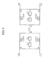
- A fourth embodiment according to the present invention will be described in detail with reference to FIG. 4 which is a diagram illustrative of a fourth optical switch having two inputs and two outputs, which is used in a novel optical add-drop multiplexer. The fourth optical switch comprises a pair of the above first novel optical switches described in the first embodiment. The two first novel optical switches are connected to each other through a first
optical transmission line 110 as a common line. If the left side one of the paired first novel optical switches is in input side and the right side one of the paired first novel optical switches is in output side, then the switching operation of the left side one of the paired first novel optical switches is carried out to select or switch any one of the two inputs of the fourth optical switch having the two inputs and the two outputs, whilst the switching operation of the right side one of the paired first novel optical switches is carried out to select or switch any one of the two outputs of the fourth optical switch having the two inputs and the two outputs, whereby the switching operations of the paired first novel optical switches realize the fourth optical switch having the two inputs and the two outputs. - Each paired first novel optical switches is exactly the same as described in the first embodiment, for which reason duplicate descriptions to the first novel optical switches will be omitted.
- As a modification to the above fourth optical switch, it is also possible that the fourth optical switch comprises a pair of the above third optical switches described in the third embodiment.
- The two fourth novel optical switches are connected to each other through a first
optical transmission lien 110 as a common line. If the left side one of the paired fourth novel optical switches is in input side and the right side one of the paired fourth novel optical switches is in output side, then the switching operation of the left side one of the paired fourth novel optical switches is carried out to select or switch any one of the two inputs of the fifth novel optical switch having the two inputs and the two outputs, whilst the switching operation of the right side one of the paired fourth novel optical switches is carried out to select or switch any one of the two outputs of the fifth novel optical switch having the two inputs and the two outputs, whereby the switching operations of the paired fourth novel optical switches realize the fifth novel optical switch having the two inputs and the two outputs. - Each of the paired fourth novel optical switches is exactly the same as described in the fourth embodiment, for which reason duplicate descriptions to the fourth novel optical switches will be omitted.
- In the above embodiment, the number of the wavelength multiplexing on each optical transmission line is one. Notwithstanding, 8, 16, 32, 64-wavelength multiplexing are available, wherein the batch-switching operation to the plural number wavelength multiplexing is carried out.
- It is also possible to set the wavelength of the optical input signal at not only 1550 nanometers but also other wavelengths, for example, 1330 nanometers.
- It is also possible to set the wavelength of the excitation light at not only 1480 nanometers or 980 nanometers but also other wavelengths provided that such wavelength is capable of exciting the impurity doped fiber. It is preferable to set the wavelength of the excitation light in consideration of both the wavelength of the optical input signal and the kind of the impurity doped fiber.
- The above excitation light switch may also be replaced by an acousto-optical switch, or a quartz-based switch.
- It is further possible to control an intensity of the optical output signal by controlling an optical power of the excitation light to be fed to the impurity doped fiber. It is possible to control the optical power of the excitation light to be fed to the impurity doped fiber by controlling an injection current to the excitation light source or by use of variable or fixed attenuator.
- It is furthermore possible to replace the erbium doped fiber by rare earth doped fiber such as tellurium doped fiber. The length of the rare earth doped fiber and a doping concentration thereof may be set in accordance with the required specifications of the optical switch.
- It is moreover possible to input the excitation light into the rare earth doped fiber in either directions or in both directions.
- It is still more possible to conduct a polarization-multiplexing to different excitation lights emitted separately from plural different excitation light sources in order to input the polarization-multiplexed excitation light into the rare earth doped fiber to obtain a high gain.
- It is yet more possible to set freely a ration of optical division at the optical coupler in accordance with the various design choices.
- The provisions of the smaller number of the excitation light source and the single excitation light switch permit ON-OFF switching operations of the plural gate switches by a simple structure. The above switch exhibits such a gain property as a sharp rising, for which reason there is substantially no influence due to a leaked light from the excitation light switch. This makes the switch available to switches having relatively large crosstalk levels such as a polymer type switch or LiNbO3 switch, thereby realizing a low crosstalk and low insertion loss optical switch. In addition, the use of the impurity doped fiber serving as an optical power amplifier can obtain a gain as the optical switch.
- A fifth embodiment according to the present invention will be described in detail with reference to FIG. 5 which is a diagram illustrative a fifth optical switch having two inputs and two outputs, which is used in a novel optical add-drop multiplexer. A structural difference of the sixth novel optical switch from the fourth optical switch is in providing a single or common excitation light source to a pair of modified first optical switches excluding individual excitation light sources described in the first embodiment.
- The fifth optical switch comprises a pair of the first novel optical switches described in the first embodiment. The two first novel optical switches are connected to each other through a first
optical transmission line 110 as a common line. The two first novel optical switches are connected are also connected to the single and common excitation light source 31 to reduce the number of the required excitation light source. If the left side one of the paired first novel optical switches is in input side and the right side one of the paired first novel optical switches is in output side, then the switching operation of the left side one of the paired first novel optical switches is carried out to select or switch any one of the two inputs of the sixth novel optical switch having the two inputs and the two outputs, whilst the switching operation of the right side one of the paired first novel optical switches is carried out to select or switch any one of the two outputs of the sixth novel optical switch having the two inputs and the two outputs, whereby the switching operations of the paired first novel optical switches realize the sixth novel optical switch having the two inputs and the two outputs. - Each of the paired first novel optical switches is the same as described in the first embodiment except for excluding the individual excitation light sources, for which reason duplicate descriptions to the first novel optical switches will be omitted.
- As a modification to the above sixth novel optical switch, it is also possible that the sixth novel optical switch comprises a pair of the above fourth novel optical switches described in the fourth embodiment. The two fourth novel optical switches are connected to each other through a first
optical transmission lien 110 as a common line. The two first novel optical switches are connected are also connected to the single and common excitation light source 31 to reduce the number of the required excitation light source. If the left side one of the paired fourth novel optical switches is in input side and the right side one of the paired fourth novel optical switches is in output side, then the switching operation of the left side one of the paired fourth novel optical switches is carried out to select or switch any one of the two inputs of the sixth novel optical switch having the two inputs and the two outputs, whilst the switching operation of the right side one of the paired fourth novel optical switches is carried out to select or switch any one of the two outputs of the sixth novel optical switch having the two inputs and the two outputs, whereby the switching operations of the paired fourth novel optical switches realize the sixth novel optical switch having the two inputs and the two outputs. - Each of the paired fourth novel optical switches is exactly the same as described in the fourth embodiment, for which reason duplicate descriptions to the fourth novel optical switches will be omitted.
- In the above embodiment, the number of the wavelength multiplexing on each optical transmission line is one. Notwithstanding, 8, 16, 32, 64-wavelength multiplexing are available, wherein the batch-switching operation to the plural number wavelength multiplexing is carried out.
- It is also possible to set the wavelength of the optical input signal at not only 1550 nanometers but also other wavelengths, for example, 1330 nanometers.
- It is also possible to set the wavelength of the excitation light at not only 1480 nanometers or 980 nanometers but also other wavelengths provided that such wavelength is capable of exciting the impurity doped fiber. It is preferable to set the wavelength of the excitation light in consideration of both the wavelength of the optical input signal and the kind of the impurity doped fiber.
- The above excitation light switch may also be replaced by an acousto-optical switch, or a quartz-based switch.
- It is further possible to control an intensity of the optical output signal by controlling an optical power of the excitation light to be fed to the impurity doped fiber. It is possible to control the optical power of the excitation light to be fed to the impurity doped fiber by controlling an injection current to the excitation light source or by use of variable or fixed attenuator.
- It is furthermore possible to replace the erbium doped fiber by rare earth doped fiber such as tellurium doped fiber. The length of the rare earth doped fiber and a doping concentration thereof may be set in accordance with the required specifications of the optical switch.
- It is moreover possible to input the excitation light into the rare earth doped fiber in either directions or in both directions.
- It is still more possible to conduct a polarization-multiplexing to different excitation lights emitted separately from plural different excitation light sources in order to input the polarization-multiplexed excitation light into the rare earth doped fiber to obtain a high gain.
- It is yet more possible to set freely a ratio of optical division at the optical coupler in accordance with the various design choices.
- The provisions of the smaller number of the excitation light source and the single excitation light switch permit ON-OFF switching operations of the plural gate switches by a simple structure. The above switch exhibits such a gain property as a sharp rising, for which reason there is substantially no influence due to a leaked light from the excitation light switch. This makes the switch available to switches having relatively large crosstalk levels such as a polymer type switch or LiNbO3 switch, thereby realizing a low crosstalk and low insertion loss optical switch. In addition, the use of the impurity doped fiber serving as an optical power amplifier can obtain a gain as the optical switch.
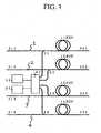
- A sixth embodiment according to the present invention will be described in detail with reference to FIG. 6 which is a diagram illustrative of a sixth optical switch having four separate optical transmission lines for separately switching optical signal transmissions on the four separate optical transmission lines, used in a novel optical add-drop multiplexer.
- The sixth optical switch has a first, second, third and fourth
optical transmission lines excitation light switch 41 having a single input connected to the excitation light source 31 and four outputs. Theexcitation light switch 41 is capable of separately ON-OFF switching operations to transmissions of the excitation lights from the four outputs. - The first
optical transmission line 1 comprises a first input sideoptical transmission line 211 and a first output sideoptical transmission line 221, wherein the first input sideoptical transmission line 211 is connected through a first erbium doped fiber 11EDF to the first input sideoptical transmission line 211. A firstoptical coupler 21 is provided on the first input sideoptical transmission line 211. The firstoptical coupler 21 is connected to a first output of theexcitation light switch 41. A first optical signal is transmitted on the first input sideoptical transmission line 211 through the first erbium doped fiber 11EDF to the first input sideoptical transmission line 211. If theexcitation light switch 41 is operated to switch ON to allow transmission of the excitation light emitted from the excitation light source 31 through the firstoptical coupler 21 to the first erbium doped fiber 11EDF, then the first erbium doped fiber 11EDF is excited to allow that the transmission of the first optical signal having been transmitted on the first input sideoptical transmission line 211 is transmitted through the first erbium doped fiber 11EDF to the first output sideoptical transmission line 221. - The second
optical transmission line 1 comprises a second input sideoptical transmission line 212 and a second output sideoptical transmission line 222, wherein the second input sideoptical transmission line 212 is connected through a second erbium doped fiber 12EDF to the second input sideoptical transmission line 212. A secondoptical coupler 22 is provided on the second input sideoptical transmission line 212. The secondoptical coupler 22 is connected to a second output of theexcitation light switch 41. A second optical signal is transmitted on the second input sideoptical transmission line 212 through the second erbium doped fiber 12EDF to the second input sideoptical transmission line 212. If theexcitation light switch 41 is operated to switch ON to allow transmission of the excitation light emitted from the excitation light source 31 through the secondoptical coupler 22 to the second erbium doped fiber 12EDF, then the second erbium doped fiber 12EDF is excited to allow that the transmission of the second optical signal having been transmitted on the second input sideoptical transmission line 212 is transmitted through the second erbium doped fiber 12EDF to the second output sideoptical transmission line 222. - The third
optical transmission line 1 comprises a third input sideoptical transmission line 213 and a third output sideoptical transmission line 223, wherein the third input sideoptical transmission line 213 is connected through a third erbium doped fiber 13EDF to the third input sideoptical transmission line 213. A thirdoptical coupler 23 is provided on the third input sideoptical transmission line 213. The thirdoptical coupler 23 is connected to a third output of theexcitation light switch 41. A third optical signal is transmitted on the third input sideoptical transmission line 213 through the third erbium doped fiber 13EDF to the third input sideoptical transmission line 213. If theexcitation light switch 41 is operated to switch ON to allow transmission of the excitation light emitted from the excitation light source 31 through the thirdoptical coupler 23 to the third erbium doped fiber 13EDF, then the third erbium doped fiber 13EDF is excited to allow that the transmission of the third optical signal having been transmitted on the third input sideoptical transmission line 213 is transmitted through the third erbium doped fiber 13EDF to the third output sideoptical transmission line 223. - The fourth
optical transmission line 1 comprises a fourth input sideoptical transmission line 214 and a fourth output sideoptical transmission line 224, wherein the fourth input sideoptical transmission line 214 is connected through a fourth erbium doped fiber 14EDF to the fourth input sideoptical transmission line 214. A fourthoptical coupler 24 is provided on the fourth input sideoptical transmission line 214. The fourthoptical coupler 24 is connected to a fourth output of theexcitation light switch 41. A fourth optical signal is transmitted on the fourth input sideoptical transmission line 214 through the fourth erbium doped fiber 14EDF to the fourth input sideoptical transmission line 214. If theexcitation light switch 41 is operated to switch ON to allow transmission of the excitation light emitted from the excitation light source 31 through the fourthoptical coupler 24 to the fourth erbium doped fiber 14EDF, then the fourth erbium doped fiber 14EDF is excited to allow that the transmission of the fourth optical signal having been transmitted on the fourth input sideoptical transmission line 214 is transmitted through the fourth erbium doped fiber 14EDF to the fourth output sideoptical transmission line 224. - The
excitation light switch 41 is capable of separate ON-OFF switching operations to the four outputs from which the excitation lights are outputted. If theexcitation light switch 41 is operated to switch ON to the four outputs, then the excitation lights are fed through the first, second, third andfourth couplers optical transmission lines excitation light switch 41 is operated to switch ON to the first, second and third outputs, then the excitation lights are fed through the first, second andthird couplers optical transmission lines excitation light switch 41 is operated to switch ON to the first and second outputs, then the excitation lights are fed through the first andsecond couplers optical transmission lines excitation light switch 41 is operated to switch ON to the first output, then the excitation lights are fed through thefirst coupler 21 to the first erbium doped fiber 11EDF, whereby the first optical signal is transmitted through the first erbium doped fiber 11EDF to the first output sideoptical transmission line 221, whilst the second, third and fourth optical signals are absorbed by the second, third and fourth erbium doped fibers 12EDF, 13EDF and 14EDF. - In the above embodiment, the number of the wavelength multiplexing on each optical transmission line is one. Notwithstanding, 8, 16, 32, 64-wavelength multiplexing are available, wherein the batch-switching operation to the plural number wavelength multiplexing is carried out.
- It is also possible to set the wavelength of the optical input signal at not only 1550 nanometers but also other wavelengths, for example, 1330 nanometers.
- It is also possible to set the wavelength of the excitation light at not only 1480 nanometers or 980 nanometers but also other wavelengths provided that such wavelength is capable of exciting the impurity doped fiber. It is preferable to set the wavelength of the excitation light in consideration of both the wavelength of the optical input signal and the kind of the impurity doped fiber.
- The above excitation light switch may also be replaced by an acousto-optical switch, or a quartz-based switch.
- It is further possible to control an intensity of the optical output signal by controlling an optical power of the excitation light to be fed to the impurity doped fiber. It is possible to control the optical power of the excitation light to be fed to the impurity doped fiber by controlling an injection current to the excitation light source or by use of variable or fixed attenuator.
- It is furthermore possible to replace the erbium doped fiber by rare earth doped fiber such as tellurium doped fiber. The length of the rare earth doped fiber and a doping concentration thereof may be set in accordance with the required specifications of the optical switch.
- It is moreover possible to input the excitation light into the rare earth doped fiber in either directions or in both directions.
- It is still more possible to conduct a polarization-multiplexing to different excitation lights emitted separately from plural different excitation light sources in order to input the polarization-multiplexed excitation light into the rare earth doped fiber to obtain a high gain.
- It is yet more possible to set freely a ration of optical division at the optical coupler in accordance with the various design choices.
- The provisions of the smaller number of the excitation light source and the single excitation light switch permit ON-OFF switching operations of the plural gate switches by a simple structure. The above switch exhibits such a gain property as a sharp rising, for which reason there is substantially no influence due to a leaked light from the excitation light switch. This makes the switch available to switches having relatively large crosstalk levels such as a polymer type switch or LiNbO3 switch, thereby realizing a low crosstalk and low insertion loss optical switch. In addition, the use of the impurity doped fiber serving as an optical power amplifier can obtain a gain as the optical switch.
- A seventh embodiment according to the present invention will be described in detail with reference to FIG. 7 which is a diagram illustrative a seventh optical switch having four separate optical transmission lines for separately switching optical signal transmissions on the four separate optical transmission lines, which is used in a novel optical add-drop multiplexer. A structural difference of the seventh optical switch from the sixth optical switch is in providing double excitation light sources and an optical cross connector serving as a switch.
- The seventh novel optical switch has first, second, third and fourth
optical transmission lines optical transmission lines - The first
optical transmission line 1 comprises a first input sideoptical transmission line 211 and a first output sideoptical transmission line 221, wherein the first input sideoptical transmission line 211 is connected through a first erbium doped fiber 11EDF to the first input sideoptical transmission line 211. A firstoptical coupler 21 is provided on the first input sideoptical transmission line 211. The firstoptical coupler 21 is connected to a first output of the optical cross connector 81. A first optical signal is transmitted on the first input sideoptical transmission line 211 through the first erbium doped fiber 11EDF to the first input sideoptical transmission line 211. If the optical cross connector 81 is operated to switch ON to allow transmission of the excitation light emitted from the excitation light source 31 through the firstoptical coupler 21 to the first erbium doped fiber 11EDF, then the first erbium doped fiber 11EDF is excited to allow that the transmission of the first optical signal having been transmitted on the first input sideoptical transmission line 211 is transmitted through the first erbium doped fiber 11EDF to the first output sideoptical transmission line 221. - The second
optical transmission line 1 comprises a second input sideoptical transmission line 212 and a second output sideoptical transmission line 222, wherein the second input sideoptical transmission line 212 is connected through a second erbium doped fiber 12EDF to the second input sideoptical transmission line 212. A secondoptical coupler 22 is provided on the second input sideoptical transmission line 212. The secondoptical coupler 22 is connected to a second output of the optical cross connector 81. A second optical signal is transmitted on the second input sideoptical transmission line 212 through the second erbium doped fiber 12EDF to the second input sideoptical transmission line 212. If the optical cross connector 81 is operated to switch ON to allow transmission of the excitation light emitted from the excitation light source 31 through the secondoptical coupler 22 to the second erbium doped fiber 12EDF, then the second erbium doped fiber 12EDF is excited to allow that the transmission of the second optical signal having been transmitted on the second input sideoptical transmission line 212 is transmitted through the second erbium doped fiber 12EDF to the second output sideoptical transmission line 222. - The third
optical transmission line 1 comprises a third input sideoptical transmission line 213 and a third output sideoptical transmission line 223, wherein the third input sideoptical transmission line 213 is connected through a third erbium doped fiber 13EDF to the third input sideoptical transmission line 213. A thirdoptical coupler 23 is provided on the third input sideoptical transmission line 213. The thirdoptical coupler 23 is connected to a third output of the optical cross connector 81. A third optical signal is transmitted on the third input sideoptical transmission line 213 through the third erbium doped fiber 13EDF to the third input sideoptical transmission line 213. If the optical cross connector 81 is operated to switch ON to allow transmission of the excitation light emitted from the excitation light source 31 through the thirdoptical coupler 23 to the third erbium doped fiber 13EDF, then the third erbium doped fiber 13EDF is excited to allow that the transmission of the third optical signal having been transmitted on the third input sideoptical transmission line 213 is transmitted through the third erbium doped fiber 13EDF to the third output sideoptical transmission line 223. - The fourth
optical transmission line 1 comprises a fourth input sideoptical transmission line 214 and a fourth output sideoptical transmission line 224, wherein the fourth input sideoptical transmission line 214 is connected through a fourth erbium doped fiber 14EDF to the fourth input sideoptical transmission line 214. A fourthoptical coupler 24 is provided on the fourth input sideoptical transmission line 214. The fourthoptical coupler 24 is connected to a fourth output of the optical cross connector 81. A fourth optical signal is transmitted on the fourth input sideoptical transmission line 214 through the fourth erbium doped fiber 14EDF to the fourth input sideoptical transmission line 214. If the optical cross connector 81 is operated to switch ON to allow transmission of the excitation light emitted from the excitation light source 31 through the fourthoptical coupler 24 to the fourth erbium doped fiber 14EDF, then the fourth erbium doped fiber 14EDF is excited to allow that the transmission of the fourth optical signal having been transmitted on the fourth input sideoptical transmission line 214 is transmitted through the fourth erbium doped fiber 14EDF to the fourth output sideoptical transmission line 224. - The optical cross connector 81 is capable of separate ON-OFF switching operations to the four outputs from which the excitation lights are outputted. If the optical cross connector 81 is operated to switch ON to the four outputs, then the excitation lights are fed through the first, second, third and
fourth couplers optical transmission lines third couplers optical transmission lines second couplers optical transmission lines first coupler 21 to the first erbium doped fiber 11EDF, whereby the first optical signal is transmitted through the first erbium doped fiber 11EDF to the first output sideoptical transmission line 221, whilst the second, third and fourth optical signals are absorbed by the second, third and fourth erbium doped fibers 12EDF,13EDF and 14EDF - The dual excitation light sources 32 and 33 increases the excitation power to be fed to the individual erbium doped fibers on the first to fourth
optical transmission lines - In the above embodiment, the number of the wavelength multiplexing on each optical transmission line is one. Notwithstanding, 8, 16, 32, 64-wavelength multiplexing are available, wherein the batch-switching operation to the plural number wavelength multiplexing is carried out.
- It is also possible to set the wavelength of the optical input signal at not only 1550 nanometers but also other wavelengths, for example, 1330 nanometers.
- It is also possible to set the wavelength of the excitation light at not only 1480 nanometers or 980 nanometers but also other wavelengths provided that such wavelength is capable of exciting the impurity doped fiber. It is preferable to set the wavelength of the excitation light in consideration of both the wavelength of the optical input signal and the kind of the impurity doped fiber.
- The above excitation light switch may also be replaced by an acousto-optical switch, or a quartz-based switch.
- It is further possible to control an intensity of the optical output signal by controlling an optical power of the excitation light to be fed to the impurity doped fiber. It is possible to control the optical power of the excitation light to be fed to the impurity doped fiber by controlling an injection current to the excitation light source or by use of variable or fixed attenuator.
- It is furthermore possible to replace the erbium doped fiber by rare earth doped fiber such as tellurium doped fiber. The length of the rare earth doped fiber and a doping concentration thereof may be set in accordance with the required specifications of the optical switch.
- It is moreover possible to input the excitation light into the rare earth doped fiber in either directions or in both directions.
- It is still more possible to conduct a polarization-multiplexing to different excitation lights emitted separately from plural different excitation light sources in order to input the polarization-multiplexed excitation light into the rare earth doped fiber to obtain a high gain.
- It is yet more possible to set freely a ration of optical division at the optical coupler in accordance with the various design choices.
- The provisions of the smaller number of the excitation light source and the single excitation light switch permit ON-OFF switching operations of the plural gate switches by a simple structure. The above switch exhibits such a gain property as a sharp rising, for which reason there is substantially no influence due to a leaked light from the excitation light switch. This makes the switch available to switches having relatively large crosstalk levels such as a polymer type switch or LiNbO3 switch, thereby realizing a low crosstalk and low insertion loss optical switch. In addition, the use of the impurity doped fiber serving as an optical power amplifier can obtain a gain as the optical switch.
Claims (2)
- An optical add-drop multiplexer comprising at least a single set of:- an input side optical transmission line (110) for transmitting a first optical signal;- an input side optical coupler (21) provided on said input side optical transmission line for dividing said first optical signal into first and second divided optical signals;- first and second optical transmission lines (120, 121) connected with said input side optical coupler for transmissions of said first and second divided optical signals respectively, said first and second optical transmission lines (120, 121) having first and second impurity doped fibers (11, 12);- an optical receiver connected through said first optical transmission line (120) to said first impurity doped fiber (11) for receiving said first divided optical signal only when said first impurity doped fiber (11) is excited;- an optical transmitter connected through said second optical transmission line (121) to said second impurity doped fiber (12) for transmitting a second optical signal through said second impurity doped fiber (12) to said input side optical transmission line (110) for output of said second optical signal only when said second impurity doped fiber (12) is excited;- at least an excitation light source (31) for emitting an excitation light; and- an excitation light switch (41) connected to said excitation light source (31) and also connected to said first and second optical transmission lines (120, 121) for selective switching operations to supply said excitation light to any one of said first and second optical transmission lines to feed said excitation light to the selected one of said first and second impurity doped fibers (11, 12), thereby causing an excitation of said selected one of said first and second impurity doped fibers (11, 12), whilst the unselected one of said first and second impurity doped fibers (11, 12) is unexcited.
- An optical add-drop multiplexer comprising a plurality of optical add-drop multiplexers according to claim 1 and further comprising an optical device having at least any one of multiplexing function and demultiplexing function so that said optical add-drop multiplexers according to claim 1 are operable to different wavelength optical signals.
Applications Claiming Priority (9)
| Application Number | Priority Date | Filing Date | Title |
|---|---|---|---|
| JP31107097 | 1997-10-28 | ||
| JP31107097A JP3219034B2 (en) | 1997-10-28 | 1997-10-28 | Optical add / drop device and optical gate switch |
| JP31107197A JP3233271B2 (en) | 1997-10-28 | 1997-10-28 | WDM optical repeater |
| JP311070/97 | 1997-10-28 | ||
| JP31107197 | 1997-10-28 | ||
| JP311071/97 | 1997-10-28 | ||
| JP29842797 | 1997-10-30 | ||
| JP298427/97 | 1997-10-30 | ||
| JP29842797A JP3165090B2 (en) | 1997-10-30 | 1997-10-30 | Light switch |
Publications (3)
| Publication Number | Publication Date |
|---|---|
| EP0914015A2 EP0914015A2 (en) | 1999-05-06 |
| EP0914015A3 EP0914015A3 (en) | 2003-03-12 |
| EP0914015B1 true EP0914015B1 (en) | 2006-12-20 |
Family
ID=27338222
Family Applications (1)
| Application Number | Title | Priority Date | Filing Date |
|---|---|---|---|
| EP98120406A Expired - Lifetime EP0914015B1 (en) | 1997-10-28 | 1998-10-28 | Optical add-drop multiplexer |
Country Status (3)
| Country | Link |
|---|---|
| US (3) | US6424440B1 (en) |
| EP (1) | EP0914015B1 (en) |
| DE (1) | DE69836670T2 (en) |
Families Citing this family (19)
| Publication number | Priority date | Publication date | Assignee | Title |
|---|---|---|---|---|
| GB2352105B (en) * | 1999-07-15 | 2001-09-26 | Marconi Comm Ltd | Optical system |
| US6792210B1 (en) * | 1999-08-23 | 2004-09-14 | Optical Coating Laboratory, Inc. | Hybrid optical add/drop multiplexing devices |
| JP2001223641A (en) * | 2000-02-14 | 2001-08-17 | Sumitomo Electric Ind Ltd | Optical transmission system and optical transmission method |
| GB2360654A (en) | 2000-03-25 | 2001-09-26 | Marconi Comm Ltd | Power controlling network element for adding new channels in a controlled manner |
| JP2002250833A (en) | 2000-12-22 | 2002-09-06 | Furukawa Electric Co Ltd:The | Optical fiber, dispersion compensator using the optical fiber and optical transmission system |
| US6556340B1 (en) * | 2001-04-06 | 2003-04-29 | Onetta, Inc. | Optical amplifiers and upgrade modules |
| GB2381683A (en) * | 2001-10-30 | 2003-05-07 | Kamelian Ltd | A re-configurable wavelength add-drop multiplexer |
| KR100442658B1 (en) * | 2002-08-14 | 2004-08-02 | 삼성전자주식회사 | Light source device for wavelength division multiplexing optical communication system |
| US8909038B2 (en) * | 2003-01-07 | 2014-12-09 | Alcatel Lucent | Method and apparatus providing transient control in optical add-drop nodes |
| US20060204169A1 (en) * | 2005-03-09 | 2006-09-14 | New Span Opto-Technology, Inc. | All-optical controllable photonic switch |
| US8305877B2 (en) * | 2009-09-10 | 2012-11-06 | Tyco Electronics Subsea Communications Llc | System and method for distributed fault sensing and recovery |
| GB201008003D0 (en) * | 2010-05-13 | 2010-06-30 | Oclaro Technology Plc | Optical Amplifiers |
| JP5614252B2 (en) * | 2010-11-12 | 2014-10-29 | 富士通株式会社 | Optical switching device and communication system |
| TWI416895B (en) * | 2010-12-07 | 2013-11-21 | Ind Tech Res Inst | A signal transmitting method for peer-to-peer optical networks and system using the same |
| JP5614327B2 (en) * | 2011-02-24 | 2014-10-29 | 日本電気株式会社 | Optical amplifier controller |
| CN104038287B (en) * | 2014-04-09 | 2017-11-03 | 国电南瑞科技股份有限公司 | It is a kind of take on the spot can ultra long haul OPGW optical fiber telecommunications systems and its implementation |
| CN108141283B (en) | 2015-09-29 | 2020-07-28 | 日本电气株式会社 | Optical repeater and control method of optical repeater |
| US10200144B1 (en) * | 2017-09-15 | 2019-02-05 | Nokia Of America Corporation | Communication system for connecting network hosts |
| US11522629B2 (en) * | 2021-01-21 | 2022-12-06 | Ciena Corporation | Channelized optical amplifiers and amplifier arrays |
Family Cites Families (65)
| Publication number | Priority date | Publication date | Assignee | Title |
|---|---|---|---|---|
| US4317614A (en) * | 1980-02-20 | 1982-03-02 | General Dynamics, Pomona Division | Fiber optic bus manifold |
| JPS59135441A (en) | 1983-12-14 | 1984-08-03 | Hitachi Ltd | Optical waveguide switch |
| JPH022768A (en) | 1988-06-16 | 1990-01-08 | Fujitsu Ltd | Optical communication method |
| JPH02291531A (en) | 1989-04-28 | 1990-12-03 | Nippon Telegr & Teleph Corp <Ntt> | Optical transmission line switch |
| JP2714692B2 (en) | 1989-06-05 | 1998-02-16 | 日本電信電話株式会社 | Wavelength multiplexing signal light separation switching device |
| US5121450A (en) * | 1989-12-22 | 1992-06-09 | Gte Laboratories Incorporated | Fiber optical Y-junction |
| JP2781633B2 (en) | 1990-01-10 | 1998-07-30 | 株式会社日立製作所 | Cell signal processing circuit and optical switch using the same |
| JP2736277B2 (en) | 1990-02-13 | 1998-04-02 | 日本電信電話株式会社 | Light switch |
| JPH03239231A (en) * | 1990-02-16 | 1991-10-24 | Sumitomo Electric Ind Ltd | Optical switch |
| JPH049929A (en) | 1990-04-27 | 1992-01-14 | Toshiba Corp | Optical switch |
| JPH04124935A (en) * | 1990-09-17 | 1992-04-24 | Canon Inc | Light communication network and optical node to be used threrein |
| GB2251957B (en) * | 1990-11-29 | 1993-12-15 | Toshiba Kk | Optical coupler |
| JP3129455B2 (en) | 1991-01-29 | 2001-01-29 | 富士通株式会社 | Optical amplifier |
| JPH04260381A (en) | 1991-02-15 | 1992-09-16 | Fujitsu Ltd | Light amplifier |
| US5181134A (en) * | 1991-03-15 | 1993-01-19 | At&T Bell Laboratories | Photonic cross-connect switch |
| JPH04362834A (en) | 1991-06-10 | 1992-12-15 | Nec Corp | Cpfsk modulation circuit and cpfsk demodulation circuit |
| JPH0529686A (en) | 1991-07-19 | 1993-02-05 | Hitachi Ltd | Optical amplifier |
| JPH0541697A (en) | 1991-08-07 | 1993-02-19 | Nec Corp | Multiplexing system |
| JPH0651252A (en) | 1992-07-28 | 1994-02-25 | Nec Corp | Light modulation method and light intensity modulator |
| US5241414A (en) * | 1992-08-21 | 1993-08-31 | At&T Bell Laboratories | Fault tolerant optical amplifier arrangement |
| IL106766A (en) * | 1992-08-28 | 1995-12-31 | Hughes Aircraft Co | Bi-directional optical fiber amplifier for missile guidance data link repeater |
| JPH06324368A (en) | 1993-05-11 | 1994-11-25 | Nippon Telegr & Teleph Corp <Ntt> | Optical fiber amplifier |
| US5579143A (en) * | 1993-06-04 | 1996-11-26 | Ciena Corporation | Optical system with tunable in-fiber gratings |
| US5473299A (en) * | 1993-12-13 | 1995-12-05 | Matsushita Electric Industrial Co., Ltd. | Horizontal linearity correction coil |
| JP3250206B2 (en) * | 1994-02-14 | 2002-01-28 | 住友電気工業株式会社 | Optical fiber amplifier |
| JP3239590B2 (en) | 1994-03-04 | 2001-12-17 | 日立電線株式会社 | Two-wavelength band amplifier and wavelength division multiplex transmission device using the same |
| US5473599A (en) | 1994-04-22 | 1995-12-05 | Cisco Systems, Incorporated | Standby router protocol |
| US5598294A (en) * | 1994-08-18 | 1997-01-28 | Matsushita Electric Industrial Co., Ltd. | Optical fiber amplifier and optical fiber communication system |
| FR2724077B1 (en) * | 1994-08-29 | 1996-09-20 | Alcatel Nv | METHOD AND ASSEMBLY FOR ORIENTATION AND AMPLIFICATION OF GUIDED OPTICAL SIGNALS |
| US5633741A (en) * | 1995-02-23 | 1997-05-27 | Lucent Technologies Inc. | Multichannel optical fiber communications |
| US5680235A (en) * | 1995-04-13 | 1997-10-21 | Telefonaktiebolaget Lm Ericsson | Optical multichannel system |
| US6297902B1 (en) * | 1995-07-05 | 2001-10-02 | Hitachi, Ltd. | Light amplification medium control method, light amplification apparatus and system using the same |
| JP2908290B2 (en) | 1995-07-21 | 1999-06-21 | 日本電気株式会社 | Optical add / drop circuit |
| IT1277397B1 (en) * | 1995-07-31 | 1997-11-10 | Pirelli Cavi S P A Ora Pirelli | WAVE LENGTH MULTIPLATION TELECOMMUNICATION SYSTEM AND METHOD WITH CONTROLLED OUTPUT CHANNEL SEPARATION |
| NL1001209C2 (en) * | 1995-09-15 | 1997-03-20 | Nederland Ptt | Optical network. |
| JPH0996785A (en) | 1995-10-02 | 1997-04-08 | Nippon Telegr & Teleph Corp <Ntt> | Semiconductor optical modulator and optical modulation circuit |
| JPH0998135A (en) | 1995-10-03 | 1997-04-08 | Matsushita Electric Ind Co Ltd | Optical transmitter-receiver and optical transmission/ reception system |
| JP3730299B2 (en) * | 1996-02-07 | 2005-12-21 | 富士通株式会社 | Optical equalization amplifier and optical equalization amplification method |
| US5751456A (en) * | 1996-02-20 | 1998-05-12 | Lucent Technologies Inc. | Multiwavelength add/drop multiplexer |
| GB9604336D0 (en) * | 1996-02-29 | 1996-05-01 | Stc Submarine Systems Ltd | Amplifier |
| JP3556379B2 (en) * | 1996-03-07 | 2004-08-18 | 富士通株式会社 | Optical transmission system |
| JPH09258148A (en) | 1996-03-21 | 1997-10-03 | Oki Electric Ind Co Ltd | Optical modulator |
| FR2747483B1 (en) * | 1996-04-15 | 1998-05-15 | Alsthom Cge Alcatel | OPTICAL AMPLIFIER WITH VARIABLE GAIN AND CONSTANT BANDWIDTH, AND SYSTEM FOR AUTOMATICALLY COMPENSATING FOR VARIATIONS IN LOSSES IN AN OPTICAL LINK, INCLUDING SUCH AN AMPLIFIER |
| US5748350A (en) * | 1996-06-19 | 1998-05-05 | E-Tek Dynamics, Inc. | Dense wavelength division multiplexer and demultiplexer devices |
| US5953141A (en) * | 1996-10-03 | 1999-09-14 | International Business Machines Corporation | Dynamic optical add-drop multiplexers and wavelength-routing networks with improved survivability and minimized spectral filtering |
| US5778118A (en) * | 1996-12-03 | 1998-07-07 | Ciena Corporation | Optical add-drop multiplexers for WDM optical communication systems |
| JP2977024B2 (en) * | 1996-12-03 | 1999-11-10 | 日本電気株式会社 | Optical circuit for wavelength division multiplexing communication and optical transmission communication system including the same |
| JPH10173597A (en) * | 1996-12-06 | 1998-06-26 | Nec Corp | Optical equalizer |
| JP3778641B2 (en) * | 1996-12-13 | 2006-05-24 | 富士通株式会社 | Optical amplifier |
| JPH10190112A (en) * | 1996-12-27 | 1998-07-21 | Mitsubishi Electric Corp | Optical amplifier |
| US5889610A (en) * | 1996-12-31 | 1999-03-30 | Lucent Technologies Inc. | Optical protection switching system |
| US5815613A (en) * | 1996-12-31 | 1998-09-29 | Lucent Technologies Inc. | Optical switched distributor |
| US5900969A (en) * | 1997-02-14 | 1999-05-04 | Lucent Technologies Inc. | Broadband flat gain optical amplifier |
| JPH1146030A (en) | 1997-05-29 | 1999-02-16 | Nec Corp | Optical signal relaying and amplifying apparatus and optical level regulator |
| JPH1146029A (en) | 1997-05-29 | 1999-02-16 | Nec Corp | Wavelength multiplex beam signal relaying and amplifying apparatus and optical level regulator |
| JP3233204B2 (en) | 1997-08-05 | 2001-11-26 | 日本電気株式会社 | Wavelength ADM device |
| US6122096A (en) * | 1997-08-29 | 2000-09-19 | Lucent Technologies Inc. | Expandable wavelength-selective and loss-less optical add/drop system |
| US6122095A (en) * | 1997-08-29 | 2000-09-19 | Lucent Technologies Inc. | Wavelength-selective and loss-less optical add/drop multiplexer |
| JP3149916B2 (en) | 1997-09-22 | 2001-03-26 | 日本電気株式会社 | WDM optical repeater |
| JPH11146030A (en) | 1997-11-07 | 1999-05-28 | Nec Corp | Method for deciding expedient master in radio conference system |
| JP3116883B2 (en) | 1997-11-07 | 2000-12-11 | 日本電気株式会社 | QAM signal receiving device |
| JPH11155700A (en) | 1997-11-28 | 1999-06-15 | Kintaroo:Kk | Rearrangeable baby bed |
| JPH11198087A (en) | 1998-01-13 | 1999-07-27 | Sony Corp | Object feeder |
| US6556547B1 (en) | 1998-12-15 | 2003-04-29 | Nortel Networks Limited | Method and apparatus providing for router redundancy of non internet protocols using the virtual router redundancy protocol |
| US6252862B1 (en) | 1999-05-20 | 2001-06-26 | Motorola, Inc. | Method and apparatus for routing packet data in a communications system |
-
1998
- 1998-10-28 EP EP98120406A patent/EP0914015B1/en not_active Expired - Lifetime
- 1998-10-28 US US09/181,620 patent/US6424440B1/en not_active Expired - Lifetime
- 1998-10-28 DE DE69836670T patent/DE69836670T2/en not_active Expired - Lifetime
-
2001
- 2001-08-28 US US09/939,665 patent/US6466344B2/en not_active Expired - Fee Related
-
2002
- 2002-08-27 US US10/227,892 patent/US7197246B2/en not_active Expired - Fee Related
Also Published As
| Publication number | Publication date |
|---|---|
| US20020003644A1 (en) | 2002-01-10 |
| US20030048507A1 (en) | 2003-03-13 |
| EP0914015A2 (en) | 1999-05-06 |
| DE69836670D1 (en) | 2007-02-01 |
| DE69836670T2 (en) | 2007-10-04 |
| EP0914015A3 (en) | 2003-03-12 |
| US7197246B2 (en) | 2007-03-27 |
| US6466344B2 (en) | 2002-10-15 |
| US6424440B1 (en) | 2002-07-23 |
Similar Documents
| Publication | Publication Date | Title |
|---|---|---|
| EP0914015B1 (en) | Optical add-drop multiplexer | |
| US6697188B2 (en) | Radiation power equalizer | |
| EP1248392B1 (en) | Optical amplifier device and bidirectional wavelength division multiplexing optical communication system using the same | |
| US6052219A (en) | Wide bandwidth Raman amplifier capable of employing pump energy spectrally overlapping the signal | |
| RU2180768C2 (en) | Switchable fiber-optic device for fiber-optic transmission system and its components | |
| EP0535590A2 (en) | Two-way repeater employing optical amplification | |
| KR900017321A (en) | Optical branch device and optical transmission line network using the same | |
| KR970009005A (en) | Optical noise reduction device due to four wave mixing | |
| US6304368B1 (en) | Broadband optical amplification system | |
| US5835260A (en) | Optical amplifier, optical amplifying method and optical transmission system using the optical amplifier | |
| US6256140B1 (en) | Optical amplifying apparatus for transmitting wavelength division multiplexed signal light and optical network apparatus with using the same | |
| JPH06342952A (en) | Optical fiber amplifier and optical fiber transmission system | |
| US20030081285A1 (en) | Transmission device having wavelength-band-specific optical amplifiers provided commonly for all transmission lines | |
| KR100396510B1 (en) | Dispersion-compensated optical fiber amplifier | |
| JPH11274625A (en) | Optical fiber amplifier and optical fiber amplifier for bidirectional optical transmission employing it | |
| KR20030072834A (en) | Dispersion compensated erbium doped fiber amplifier | |
| US20020159138A1 (en) | Access device for pump source in cascade erbium-doped fiber amplification | |
| EP0739103A2 (en) | Bidirectional optical amplifier using an active fibre | |
| JP2001168441A (en) | Optical amplifier | |
| WO1996029627A1 (en) | Optical fiber amplifier | |
| JPH1174595A (en) | Optical fiber amplifier | |
| JPH11112065A (en) | Optical fiber amplifier | |
| JP3239590B2 (en) | Two-wavelength band amplifier and wavelength division multiplex transmission device using the same | |
| JP2714692B2 (en) | Wavelength multiplexing signal light separation switching device | |
| JPH10107351A (en) | Er-doped optical fiber amplifier for bidirectional transmission |
Legal Events
| Date | Code | Title | Description |
|---|---|---|---|
| PUAI | Public reference made under article 153(3) epc to a published international application that has entered the european phase |
Free format text: ORIGINAL CODE: 0009012 |
|
| AK | Designated contracting states |
Kind code of ref document: A2 Designated state(s): AT BE CH CY DE DK ES FI FR GB GR IE IT LI LU MC NL PT SE |
|
| AX | Request for extension of the european patent |
Free format text: AL;LT;LV;MK;RO;SI |
|
| PUAL | Search report despatched |
Free format text: ORIGINAL CODE: 0009013 |
|
| RIC1 | Information provided on ipc code assigned before grant |
Ipc: 7H 04B 10/213 B Ipc: 7H 04J 14/02 B Ipc: 7H 04Q 11/00 A |
|
| AK | Designated contracting states |
Kind code of ref document: A3 Designated state(s): AT BE CH CY DE DK ES FI FR GB GR IE IT LI LU MC NL PT SE Designated state(s): AT BE CH CY DE DK ES FI FR GB GR IE IT LI LU MC NL PT SE |
|
| AX | Request for extension of the european patent |
Extension state: AL LT LV MK RO SI |
|
| 17P | Request for examination filed |
Effective date: 20030210 |
|
| 17Q | First examination report despatched |
Effective date: 20031010 |
|
| AKX | Designation fees paid |
Designated state(s): DE FR GB IT |
|
| GRAP | Despatch of communication of intention to grant a patent |
Free format text: ORIGINAL CODE: EPIDOSNIGR1 |
|
| RTI1 | Title (correction) |
Free format text: OPTICAL ADD-DROP MULTIPLEXER |
|
| GRAS | Grant fee paid |
Free format text: ORIGINAL CODE: EPIDOSNIGR3 |
|
| GRAA | (expected) grant |
Free format text: ORIGINAL CODE: 0009210 |
|
| AK | Designated contracting states |
Kind code of ref document: B1 Designated state(s): DE FR GB IT |
|
| PG25 | Lapsed in a contracting state [announced via postgrant information from national office to epo] |
Ref country code: IT Free format text: LAPSE BECAUSE OF FAILURE TO SUBMIT A TRANSLATION OF THE DESCRIPTION OR TO PAY THE FEE WITHIN THE PRE;WARNING: LAPSES OF ITALIAN PATENTS WITH EFFECTIVE DATE BEFORE 2007 MAY HAVE OCCURRED AT ANY TIME BEFORE 2007. THE CORRECT EFFECTIVE DATE MAY BE DIFFERENT FROM THE ONE RECORDED.SCRIBED TIME-LIMIT Effective date: 20061220 |
|
| REG | Reference to a national code |
Ref country code: GB Ref legal event code: FG4D |
|
| REF | Corresponds to: |
Ref document number: 69836670 Country of ref document: DE Date of ref document: 20070201 Kind code of ref document: P |
|
| ET | Fr: translation filed | ||
| PLBE | No opposition filed within time limit |
Free format text: ORIGINAL CODE: 0009261 |
|
| STAA | Information on the status of an ep patent application or granted ep patent |
Free format text: STATUS: NO OPPOSITION FILED WITHIN TIME LIMIT |
|
| 26N | No opposition filed |
Effective date: 20070921 |
|
| REG | Reference to a national code |
Ref country code: FR Ref legal event code: PLFP Year of fee payment: 18 |
|
| PGFP | Annual fee paid to national office [announced via postgrant information from national office to epo] |
Ref country code: FR Payment date: 20150908 Year of fee payment: 18 |
|
| PGFP | Annual fee paid to national office [announced via postgrant information from national office to epo] |
Ref country code: GB Payment date: 20151028 Year of fee payment: 18 Ref country code: DE Payment date: 20151020 Year of fee payment: 18 |
|
| REG | Reference to a national code |
Ref country code: DE Ref legal event code: R119 Ref document number: 69836670 Country of ref document: DE |
|
| GBPC | Gb: european patent ceased through non-payment of renewal fee |
Effective date: 20161028 |
|
| REG | Reference to a national code |
Ref country code: FR Ref legal event code: ST Effective date: 20170630 |
|
| PG25 | Lapsed in a contracting state [announced via postgrant information from national office to epo] |
Ref country code: FR Free format text: LAPSE BECAUSE OF NON-PAYMENT OF DUE FEES Effective date: 20161102 Ref country code: GB Free format text: LAPSE BECAUSE OF NON-PAYMENT OF DUE FEES Effective date: 20161028 Ref country code: DE Free format text: LAPSE BECAUSE OF NON-PAYMENT OF DUE FEES Effective date: 20170503 |