EP0911940A1 - Adaptive Ladeschaltung für Akkumulator oder Batterie - Google Patents
Adaptive Ladeschaltung für Akkumulator oder Batterie Download PDFInfo
- Publication number
- EP0911940A1 EP0911940A1 EP98402437A EP98402437A EP0911940A1 EP 0911940 A1 EP0911940 A1 EP 0911940A1 EP 98402437 A EP98402437 A EP 98402437A EP 98402437 A EP98402437 A EP 98402437A EP 0911940 A1 EP0911940 A1 EP 0911940A1
- Authority
- EP
- European Patent Office
- Prior art keywords
- voltage
- terminals
- accumulator
- circuit
- battery
- Prior art date
- Legal status (The legal status is an assumption and is not a legal conclusion. Google has not performed a legal analysis and makes no representation as to the accuracy of the status listed.)
- Withdrawn
Links
Images

Classifications
-
- H—ELECTRICITY
- H02—GENERATION; CONVERSION OR DISTRIBUTION OF ELECTRIC POWER
- H02J—CIRCUIT ARRANGEMENTS OR SYSTEMS FOR SUPPLYING OR DISTRIBUTING ELECTRIC POWER; SYSTEMS FOR STORING ELECTRIC ENERGY
- H02J7/00—Circuit arrangements for charging or depolarising batteries or for supplying loads from batteries
Definitions
- the present invention relates to a load matching circuit for accumulator; it also relates to a battery containing such an adaptation circuit dump.
- Accumulators, and in particular Li-ion accumulators find employment growing in number of household and office devices, and particularly in Cellphones.
- the charging voltage of such devices is conventionally of 4.2 volts, and conventional chargers for this type of battery are usually provided for a corresponding charging voltage.
- the invention aims to solve the new problem of charging different accumulators using the same charger, and in particular the problem of charging 4.2, 4.1 and 4.0 volt lithium batteries with charge voltage using chargers existing at 4.2 volts.
- the present invention provides an original and simple solution to this problem. It provides a low cost solution, easily adaptable to all types accumulators.
- the invention provides a circuit for adapting the voltage of charge for an accumulator, comprising connection terminals of a accumulator, connected to output terminals, a variable resistor mounted between a connection terminals and one of the output terminals, and comparison means mounted between the connection terminals controlling the variable resistance as a function of the results of the comparison of the voltage between the connection terminals and of a nominal voltage.
- the comparison means control the variable resistance of so that the voltage between the connection terminals is equal to the nominal voltage.
- the circuit comprises a diode mounted in parallel with the variable resistance, the diode passing from the connection terminal to the exit.
- variable resistor consists of a transistor, preferably a MOSFET transistor.
- the comparison means may include an operational amplifier comparing the voltage between the connection terminals and the voltage supplied by a source Of voltage.
- They can also include a voltage divider connected between the terminals of connection, a voltage source, and an operational amplifier comparing the voltage supplied by the voltage divider and the voltage supplied by the voltage source.
- the invention also relates to a battery comprising at least one accumulator and a load voltage adaptation circuit, the circuit comprising terminals for connection connected to the terminals of the accumulator (s), connected to output terminals, a variable resistor mounted between one of the connection terminals and one of the output, and comparison means mounted between the connection terminals controlling the variable resistance according to the results of the comparison of the voltage between the connection terminals and a nominal voltage.
- the nominal voltage is the nominal charging voltage of the accumulator.
- the adaptation circuit is preferably an integrated circuit mounted on a housing of drums.
- the comparison means control the variable resistance so that the voltage between the terminals of the accumulators is equal to the nominal voltage.
- the circuit comprises a diode mounted in parallel to the variable resistor, the diode passing from the connection terminal to the output terminal.
- variable resistance consists of a transistor, preferably a MOSFET transistor.
- the comparison means may include an operational amplifier comparing the voltage between the terminals of the accumulator (s) and the voltage supplied by a source of tension. They can also include a connected voltage divider between the connection terminals, a voltage source, and an operational amplifier comparing the voltage supplied by the voltage divider and the voltage supplied by the source of tension.
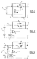
- Figure 1 shows a schematic representation of a circuit 1 for adapting the charging voltage according to the invention. This circuit makes it possible to adapt the charging voltage of a charger having a charging voltage greater than the nominal charging voltage of the accumulator.
- the circuit has two terminals 2 and 3, called connection terminals, intended for be connected respectively to the negative and positive terminals of an accumulator 4, and two terminals 6 and 7, called output terminal, intended to be connected respectively to the negative and positive terminals of a charger not shown in the figure.
- the circuit has between terminals 3 and 7 a variable resistor 8; between terminals 2 and 3, i. e. in parallel with the accumulator, means 10 for comparing the voltage at the terminals of the accumulator and of the charging voltage adapted to the accumulator; in depending on the results of the comparison, the comparison means control the variable resistance 8.
- the operation of the circuit of Figure 1 is as follows; when the accumulator 4 and the charger are respectively connected to the terminals of circuit 1, the means of comparison compare the voltage across the battery with the charging voltage nominal of the accumulator; based on the results of the comparison they control the value of the variable resistor 8; the application of variable resistance 8 reduces the voltage across the battery so that it takes the value of the nominal charging voltage. So throughout the charge of the accumulator, and whatever the charging current, the voltage across the terminals of the accumulator remains less than or equal to the nominal charging voltage.
- the charging current in this case typically varies between 0.005 and 2 amps.
- the variable resistor 8 can vary between 0 and 20 ohms, so as to induce a drop of 0.1 volts voltage.
- the circuit of Figure 1 allows, at the charge of the accumulator, to apply to this correct charging voltage. It influences neither the time nor the current of charge.
- the circuit can be adapted to existing accumulator models, and does not require not to provide an additional pin on them for the identification of the battery, or to allow separate charging and discharging.
- the size of the circuit of Figure 1 allows it to be installed on the housing of an accumulator, so as to be able to adapt the accumulator to a charger operating at a voltage greater than the nominal charging voltage of the accumulator.
- the adapter circuit has only a size of 1 cm 2 by 1.75 mm thick.
- circuit 1 advantageously has, in parallel with the resistor variable 8, a diode 12 mounted so as to allow the passage of the flowing current from terminal 3 to terminal 7.
- the adaptation circuit of figure 1 we can directly connect the device to supply to terminals 6 and 7 of the adaptation circuit: the accumulator then discharges normally, through diode 12; this only induces a minimum voltage drop.
- the circuit can also operate without diode 12, as long as the voltage the discharge of the accumulator is significantly lower than the nominal voltage of charge; therefore, from the start of the discharge, the means of comparison regulate the variable resistance at a low or zero value. The voltage drop across the variable resistance is then minimal.
- the invention makes it possible to supply batteries or accumulators of different types, with a single charger model, while ensuring that the different accumulators are charged at the nominal charging voltage.
- Figure 2 shows a schematic representation of another mode of production of a load voltage adaptation circuit according to the invention
- the Identical references to those in FIG. 1 designate the same elements, which are not not described again.
- the means of comparison include an operational amplifier 15, and a reference voltage 16; terminal non-inverting amplifier 15 is connected to terminal 3 connected to the positive terminal of the accumulator; the inverting input of the amplifier is connected to the positive terminal of the reference voltage 16.
- the negative terminal of the reference voltage is connected to the terminal 4 connected to the negative terminal of the accumulator.
- the output terminal of the operational amplifier is connected to the variable resistor 8.
- the means of comparison are mounted in parallel to the accumulator and include a operational amplifier mounted as a comparator, in series with a voltage source providing the nominal charging voltage of the accumulator.
- This source of tension may be constituted by a semiconductor device known per se, which polarizes at the nominal battery charging voltage.
- the variable resistor 8 can for example be constituted by a transistor, by example a MOSFET transistor.
- the size of the transistor is adapted to the voltage drop desired, and the current supplied by the charger.
- a MOSFET transistor is particularly advantageous, insofar as the diode 12 is integrated into the transistor and should not be added.
- FIG. 3 shows a schematic representation of another embodiment of a circuit for adapting the load voltage according to the invention.
- the circuit of Figure 3 is identical to that of Figure 2, except that the non-inverting input of the operational amplifier is connected to the connection terminal 3, not directly, but through a resistance bridge acting as a voltage divider. More specifically, two resistors 13 and 14 in series are mounted between the connection terminals, and the non-inverting input of the operational amplifier is connected between the two resistors 13 and 14.
- the assembly of FIG. 3 compares the voltage supplied by reference 16 to the product of the voltage between the connection terminals by a factor R 14 / (R 13 + R 14 ), R 13 and R 14 being the values of resistors 13 and 14.
- circuit of FIG. 3 is similar to that of the circuit of the Figure 2.
- resistors has the following advantages. Of a apart, it is possible to use the same assembly for values different from the nominal battery charge voltage: it suffices to vary the values relative of the two resistances, without it being necessary to modify the source of voltage.
- the assembly of Figure 3 allows the use of a voltage source 16 current, which delivers a voltage of 1.25 or 2.5 volts; appropriate choices of resistors 13 and 14 allow the nominal load voltage to be adjusted the accumulator.
- Figure 4 shows a diagram of a battery according to the invention, open, which includes a load matching circuit according to the invention, and, in the example of the figure, a single accumulator.
- Figure 4 shows the housing 17 of the battery, with its two terminals 18 and 19.
- an accumulator 20 In the battery case are arranged an accumulator 20 and a circuit adaptation of the load 21.
- the output terminals 6 and 7 of the adaptation circuit of load are respectively connected to terminals 18 and 19 of the battery; the terminals of circuit connection are connected to the battery terminals.
- a connection terminal of the load matching circuit which is connected to the the accumulator by a welded jumper 22.
- the other connection terminal is connected to the pole located on top of the accumulator, as shown in contact 23.
- the choice of connection terminal depends on the type of accumulator, with negative or positive pole at bucket.
- the circuit and the accumulator are mounted in the battery case by gluing or by any similar technique. It is clear that we can in the same way predict several accumulators in series in a battery.
- some lithium batteries have protection circuits: in this case you can integrate the adaptation circuit of the invention with or on the already existing protection circuit.
- variable resistance could as well be disposed between terminals 2 and 6, without the operation of the circuit being modified.
- the inverting input of the amplifier could be connected to the reference voltage source through a voltage divider assembly: the set of the source and the voltage divider would form a reference voltage source easily adjustable.
Landscapes
- Engineering & Computer Science (AREA)
- Power Engineering (AREA)
- Charge And Discharge Circuits For Batteries Or The Like (AREA)
- Secondary Cells (AREA)
Applications Claiming Priority (2)
| Application Number | Priority Date | Filing Date | Title |
|---|---|---|---|
| FR9713288 | 1997-10-23 | ||
| FR9713288A FR2770346B1 (fr) | 1997-10-23 | 1997-10-23 | Circuit d'adaptation de charge pour accumulateur ou batterie |
Publications (1)
| Publication Number | Publication Date |
|---|---|
| EP0911940A1 true EP0911940A1 (de) | 1999-04-28 |
Family
ID=9512553
Family Applications (1)
| Application Number | Title | Priority Date | Filing Date |
|---|---|---|---|
| EP98402437A Withdrawn EP0911940A1 (de) | 1997-10-23 | 1998-10-05 | Adaptive Ladeschaltung für Akkumulator oder Batterie |
Country Status (6)
| Country | Link |
|---|---|
| US (1) | US6002239A (de) |
| EP (1) | EP0911940A1 (de) |
| JP (1) | JPH11206033A (de) |
| KR (1) | KR19990037303A (de) |
| FR (1) | FR2770346B1 (de) |
| TW (1) | TW398088B (de) |
Families Citing this family (11)
| Publication number | Priority date | Publication date | Assignee | Title |
|---|---|---|---|---|
| JPH11149946A (ja) * | 1997-11-14 | 1999-06-02 | Nec Saitama Ltd | Li−ion二次電池パック、同パック用充電器、同パック用充電方法、同パック用充電システム |
| EP0988685A4 (de) * | 1998-01-31 | 2002-10-23 | John W Oglesbee | Zusätzliche batterieüberladungsschutzvorrichtung |
| US7205672B1 (en) | 2001-12-05 | 2007-04-17 | National Semiconductor Corporation | Flip chip mounted to thermal sensing element through the back side of the chip |
| CA2366030A1 (en) * | 2001-12-20 | 2003-06-20 | Global E Bang Inc. | Profiling system |
| US6492792B1 (en) | 2002-05-26 | 2002-12-10 | Motorola, Inc | Battery trickle charging circuit |
| JP4724047B2 (ja) * | 2006-05-30 | 2011-07-13 | パナソニック株式会社 | 充電システム、電池パックおよびその充電方法 |
| WO2007148745A1 (ja) * | 2006-06-22 | 2007-12-27 | Fdk Corporation | 多直列蓄電セル、直列蓄電セル装置、直列セルの電圧バランス補正回路 |
| TWI390820B (zh) * | 2009-12-01 | 2013-03-21 | Acer Inc | Charging circuit |
| JP6055298B2 (ja) * | 2012-12-14 | 2016-12-27 | ローム株式会社 | シャント回路、充電システム、及び集積回路 |
| KR20170026533A (ko) | 2014-07-02 | 2017-03-08 | 펠리온 테크놀로지스 인크. | 다중-전극 전기화학 전지 및 이를 제조하는 방법 |
| CN111884285A (zh) * | 2020-08-25 | 2020-11-03 | 湖南炬神电子有限公司 | 一种充电器及电压输出方法 |
Citations (4)
| Publication number | Priority date | Publication date | Assignee | Title |
|---|---|---|---|---|
| DE4225746A1 (de) * | 1992-08-04 | 1994-02-10 | Hagen Batterie Ag | Schaltungsvorrichtung |
| EP0665628A2 (de) * | 1994-02-01 | 1995-08-02 | Sun Microsystems, Inc. | Intelligentes Batteriesystem und Schnittstelle |
| US5623196A (en) * | 1994-12-27 | 1997-04-22 | Motorola, Inc. | Apparatus and method of simulating high battery temperature in a rechargeable battery |
| US5645949A (en) * | 1994-09-12 | 1997-07-08 | Apple Computer, Inc. | Battery cell having an internal circuit for controlling its operation |
Family Cites Families (3)
| Publication number | Priority date | Publication date | Assignee | Title |
|---|---|---|---|---|
| US4056764A (en) * | 1974-06-03 | 1977-11-01 | Nissan Motor Company, Limited | Power supply system having two different types of batteries and current-limiting circuit for lower output battery |
| NZ188610A (en) * | 1977-11-04 | 1982-08-17 | Minitronics Pty Ltd | Current integrating battery charger circuit |
| US5488284A (en) * | 1992-09-30 | 1996-01-30 | Dallas Semiconductor Corporation | Battery charger systems and methods |
-
1997
- 1997-10-23 FR FR9713288A patent/FR2770346B1/fr not_active Expired - Fee Related
- 1997-11-04 US US08/964,456 patent/US6002239A/en not_active Expired - Fee Related
-
1998
- 1998-10-05 EP EP98402437A patent/EP0911940A1/de not_active Withdrawn
- 1998-10-19 TW TW087117266A patent/TW398088B/zh not_active IP Right Cessation
- 1998-10-22 JP JP10301228A patent/JPH11206033A/ja active Pending
- 1998-10-22 KR KR1019980044333A patent/KR19990037303A/ko not_active Application Discontinuation
Patent Citations (4)
| Publication number | Priority date | Publication date | Assignee | Title |
|---|---|---|---|---|
| DE4225746A1 (de) * | 1992-08-04 | 1994-02-10 | Hagen Batterie Ag | Schaltungsvorrichtung |
| EP0665628A2 (de) * | 1994-02-01 | 1995-08-02 | Sun Microsystems, Inc. | Intelligentes Batteriesystem und Schnittstelle |
| US5645949A (en) * | 1994-09-12 | 1997-07-08 | Apple Computer, Inc. | Battery cell having an internal circuit for controlling its operation |
| US5623196A (en) * | 1994-12-27 | 1997-04-22 | Motorola, Inc. | Apparatus and method of simulating high battery temperature in a rechargeable battery |
Non-Patent Citations (1)
| Title |
|---|
| GARRETT S M: "APPARATUS FOR CHARGING A LITHIUM ION BATTERY IN A NICKEL SYSTEM CHARGER", MOTOROLA TECHNICAL DEVELOPMENTS, vol. 28, August 1996 (1996-08-01), pages 95 - 97, XP000638432 * |
Also Published As
| Publication number | Publication date |
|---|---|
| FR2770346A1 (fr) | 1999-04-30 |
| KR19990037303A (ko) | 1999-05-25 |
| TW398088B (en) | 2000-07-11 |
| FR2770346B1 (fr) | 1999-12-03 |
| US6002239A (en) | 1999-12-14 |
| JPH11206033A (ja) | 1999-07-30 |
Similar Documents
| Publication | Publication Date | Title |
|---|---|---|
| EP0110775B1 (de) | Regulierungseinrichtung mit kleiner Verlustspannung | |
| EP1366402B1 (de) | Spannungsregler mit kurzschlussschutz | |
| EP0691725B1 (de) | Regelungsvorrichtung für eine elektrische Akkumulatorbatterie | |
| EP0573832B1 (de) | Gerät zum Laden eines wiederaufladbaren Akkumulators | |
| EP0012315A1 (de) | Verfahren und Vorrichtung zur Überwachung des Ladezustandes eines Akkumulators | |
| EP0911940A1 (de) | Adaptive Ladeschaltung für Akkumulator oder Batterie | |
| EP2600462B1 (de) | Verfahren zum Ausgleich von Spannungen elektrischer Elemente, die auf mehreren parallelen Zweigen angeordnet sind | |
| EP1936541A1 (de) | Ein/aus Batterieladegerät mit Versorgungsschutzschaltung für eine monolithische integrierte Schaltung die verwendet die Energie von der Antenne | |
| WO2014033397A1 (fr) | Dispositf de detection et de mesure d'un defaut d'isolement | |
| EP3171482B1 (de) | Elektrische batterie, die ein elektronisches steuerungssystem umfasst | |
| FR2548403A1 (fr) | Stabilisateur de tension integre monolithique a domaine d'utilisation etendu, pour des applications de type automobile | |
| AU724298B2 (en) | Battery charging system | |
| FR2672705A1 (fr) | Circuit generateur d'une tension de reference variable en fonction de la temperature, notamment pour regulateur de la tension de charge d'une batterie par un alternateur. | |
| EP1381131A1 (de) | Verbesserte Schutzeinrichtung mit 1S Schaltungen für elektrochemische Batterienanordnungen | |
| EP1383222B1 (de) | Batterielader | |
| FR2724501A1 (fr) | Appareil egaliseur de charge pour des batteries connectees en serie | |
| CA2571623C (fr) | Procede de gestion de l'alimentation electrique et circuit d'alimentation electrique d'un appareil | |
| EP0544566B1 (de) | Stromquellenkontrollmodul für Batteriekontrolleinheit und Batterie mit diesem Modul | |
| FR2786623A1 (fr) | Procede de commande de charge et de decharge | |
| EP0505234B1 (de) | Schaltkreis zur Erkennung eines Schalterzustandes, namentlich eines Zündschlüssels in einem Spannungsregler eines Wechselstromgenerators | |
| FR2611283A1 (fr) | Dispositif comportant un circuit electronique de traitement d'un signal analogique | |
| EP0809342A1 (de) | Anordnung zur Regelung der Ladung einer modularen Einheit von elektrochemischen Zellen, die in Reihe geschaltet sind und entsprechendes Modul zur Messung der Zellen | |
| EP1850446A1 (de) | Verfahren zur Batterieaufladung mit Kompensation des inneren Widerstands, Aufladegerät und Batterie zur Umsetzung dieses Verfahrens | |
| FR2858485A1 (fr) | Dispositif pour charger une batterie | |
| EP0163332B1 (de) | Statisches Relais für Gleichstrom |
Legal Events
| Date | Code | Title | Description |
|---|---|---|---|
| PUAI | Public reference made under article 153(3) epc to a published international application that has entered the european phase |
Free format text: ORIGINAL CODE: 0009012 |
|
| AK | Designated contracting states |
Kind code of ref document: A1 Designated state(s): DE FR GB |
|
| AX | Request for extension of the european patent |
Free format text: AL;LT;LV;MK;RO;SI |
|
| 17P | Request for examination filed |
Effective date: 19991028 |
|
| AKX | Designation fees paid |
Free format text: DE FR GB |
|
| RAP1 | Party data changed (applicant data changed or rights of an application transferred) |
Owner name: SAFT FINANCE S.AE.R.L. |
|
| STAA | Information on the status of an ep patent application or granted ep patent |
Free format text: STATUS: THE APPLICATION IS DEEMED TO BE WITHDRAWN |
|
| 18D | Application deemed to be withdrawn |
Effective date: 20070503 |