EP0911636A2 - Appareil d'échantillonnage électro-optique - Google Patents
Appareil d'échantillonnage électro-optique Download PDFInfo
- Publication number
- EP0911636A2 EP0911636A2 EP98308145A EP98308145A EP0911636A2 EP 0911636 A2 EP0911636 A2 EP 0911636A2 EP 98308145 A EP98308145 A EP 98308145A EP 98308145 A EP98308145 A EP 98308145A EP 0911636 A2 EP0911636 A2 EP 0911636A2
- Authority
- EP
- European Patent Office
- Prior art keywords
- electro
- conductive path
- optic
- electric
- laser beam
- Prior art date
- Legal status (The legal status is an assumption and is not a legal conclusion. Google has not performed a legal analysis and makes no representation as to the accuracy of the status listed.)
- Withdrawn
Links
Images

Classifications
-
- G—PHYSICS
- G01—MEASURING; TESTING
- G01R—MEASURING ELECTRIC VARIABLES; MEASURING MAGNETIC VARIABLES
- G01R13/00—Arrangements for displaying electric variables or waveforms
- G01R13/20—Cathode-ray oscilloscopes
- G01R13/22—Circuits therefor
- G01R13/34—Circuits for representing a single waveform by sampling, e.g. for very high frequencies
Definitions
- This invention relates to electro-optic sampling apparatuses that are provided for oscilloscopes to perform measurement on measured objects with respect to electric potentials of signals having high frequencies, which are higher than 5 GHz, for example.
- This application is based on Patent Application No. Hei 9-273154 filed in Japan, the content of which is incorporated herein by reference.
- oscilloscopes are widely used for measurement of waveforms with regard to rapidly varying electric phenomena.
- the recent technology does not provide probes whose impedance is sufficiently high. So, it does not provide the high-precision oscilloscope which is capable of measuring electric potentials of signals having high frequency ranges, which reach 5 GHz or so.
- a high-impedance probe of a handy type is provided to enable measurement on potentials of signals of the measured circuits without imparting disturbances to the measured circuits mounted on the printed-circuit board of the information communication system.
- This high-impedance probe has a metal rod, which is brought into contact with a conductive path (e.g., microstrip line).
- the metal rod is attached to one end of electro-optic material, which is made of BSO (i.e., Bi 12 SiO 20 ) and to which a dielectric mirror is attached. So, signals on the microstrip line is detected by the metal rod as in form of potentials detected between ends of the electro-optic material.
- birefringence ratio of light is varied in response to variations of electric field strength corresponding to the detected potentials.
- Incoming laser beams, which are incident on the electro-optic material, are varied in polarization in accordance with variations of the birefringence ratio.
- a polarization detection optical system of a probe module extracts such variations in polarization of the laser beams so as to process them. Thus, it is possible to perform measurement on voltages of the signals of the measured circuits.
- the conventional high-impedance probe is capable of measuring voltages of signals having high frequencies, which are higher than 5 GHz or so.
- a measurement point corresponds to a "bare" conductive portion such as the microstrip line that the aforementioned metal rod is brought into “direct” contact with.
- the conventional technology suffers from a problem that it is impossible to directly detect potentials of signals transmitted on a conductor (or core line) of a coaxial cable that provides interconnection between circuits, for example.
- an electric input connector inputs a measured electric signal, which is introduced to a conductive path such as a microstrip line.
- An electro-optic material e.g., Bi 12 SiO 20
- An electro-optic effect such as Pockel's effect is fixed to a bare portion of the conductive path and is varied in birefringence ratio in response to strength of electric field generated by the conductive path through which the measured electric signal transmits.
- the conductive path is then terminated by a terminal device. Now, a laser beam is radiated toward the electro-optic material, wherein it is varied in polarization in response to variations of the birefringence ratio.
- the laser beam is reflected by a dielectric mirror and is separated into two beams by a polarization beam splitter.
- Photodiodes are provided to convert the two beams to electric signals representing potentials.
- voltage of the measured electric signal is measured based on the electric signals.
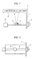
- FIG. 1 is a front view showing essential parts of an electro-optic sampling apparatus in accordance with the preferred embodiment of the invention.
- FIG. 2 is a side view showing the electro-optic sampling apparatus.
- reference symbol “1” designates a front panel of an oscilloscope, which is equipped with an electric input connector 2 for external input sampling.
- a conductive path 3 containing a elongated conductor is connected to the electric input connector 2.
- the conductor is made “bare” along an overall area of the conductive path 3 or at a selected part of the conductive path 3. So, an electro-optic material 4 is fixed in such a way that it is brought into “tight” contact with a bare portion of the conductive path 3 in advance.
- the electro-optic material 4 is used for the electro-optic material 4. Being influenced by electric field produced by the conductive path 3, the electro-optic material 4 causes Pockel's effect corresponding to electro-optical effect. Due to the Pockel's effect, the electro-optic material 4 functions to vary birefringence ratio in response to electric field strength. As shown in FIG. 3, laser beams generated by a light source 7 are incident on the electro-optic material 4 under the Pockel's effect. Thus, the laser beam is varied in polarization in response to variations of the birefringence ratio of the electro-optic material 4. Then, such varied laser beam is reflected by a dielectric mirror (not shown), which in turn provides reflected laser beam.
- a dielectric mirror not shown
- a polarization beam splitter (not shown) is arranged at a selected position with a certain distance from the middle of the path that the incoming laser beam progresses.
- the reflected laser beam is separated by the polarization beam splitter to provide separated laser beams.
- the separated laser beams are converted to electric signals (or potential signals) respectively by photodiodes constructing a light detection unit 8 show in FIG. 3.
- the light detection unit 8 outputs two potential signals, which are then processed by a voltage measurement device 9.
- a voltage measurement device 9 thus, it is possible to perform measurement on the voltage of the signal input from the external via the electric input connector 2.
- a terminal device 5 is arranged at an opposite end of the conductive path 3, which is opposite to the end corresponding to the electric input connector 2. Using the terminal device 5, it is possible to perform measurement on the voltage of the signal transmitted through the low-impedance coaxial cable and the like. Termination of the conductive path 3 is made as shown in FIG. 3. That is, the conductive path 3 can be terminated by the terminal device 5, which is equipped inside of the front pane 1. Or, it can be terminated by an external terminal device 10, which is connected to the conductive path 3 via an electric output connector 6. By making adjustment on impedance of the electric circuit as described above, it is possible to avoid occurrence of measurement error due to interference and loss which are caused by reflection and transmission of electric signals.
- the electro-optic sampling apparatus it is possible to introduce measured electric signals, given from the external, into the electro-optic sampling apparatus by merely connecting an external connector (not shown) to the electric input connector 2. Therefore, it is possible to transmit the measured electric signals onto the conductive path 3 such as the microstrip line on the printed-circuit board with high performance, for example.
- the electric-optic material 4 is fixed to the conductive path 3 in advance. For this reason, a constant contact area can be established between the electro-optic material 4 and the conductive path 3. Further, it is possible to suppress transmission loss of the electric signals to be about a prescribed low value.
- the electro-optic material 4 is connected directly with electric field that is caused by electric signals propagating through the conductive path 3. Due to the electro-optic effect such as the Pockel's effect, the electro-optic material 4 is varied in birefringence ratio in response to strength of the "connected" electric field.
- the laser beam is varied in polarization when being incident on the electro-optic material 4. Such polarization-varied laser beam is reflected by the dielectric mirror and is then separated by the beam splitter, so that the separated beams are input to the photodiodes. Then, the photodiodes convert the beams to electric signals, which are input to the voltage measurement device 9.
- the electro-optic material 4 is configured to detect potential difference between end surfaces thereof. So, sensitivity in detection of the potential difference can be improved by connecting a grounded electrode to a first end surface of the electro-optic material 4, which is opposite to a second end surface brought in contact with the conductive path 3.
- the present embodiment has a configuration that electro-optic crystal is mounted on the microstrip line.
- electro-optic crystal is mounted on the microstrip line.
- another type of the microstrip line such as GaAs board and InP board, which has electro-optic effect by itself.
Landscapes
- Physics & Mathematics (AREA)
- General Physics & Mathematics (AREA)
- Tests Of Electronic Circuits (AREA)
- Measuring Instrument Details And Bridges, And Automatic Balancing Devices (AREA)
- Measurement Of Current Or Voltage (AREA)
Applications Claiming Priority (3)
| Application Number | Priority Date | Filing Date | Title |
|---|---|---|---|
| JP273154/97 | 1997-10-06 | ||
| JP9273154A JPH11108962A (ja) | 1997-10-06 | 1997-10-06 | 電気光学サンプリング装置 |
| JP27315497 | 1997-10-06 |
Publications (2)
| Publication Number | Publication Date |
|---|---|
| EP0911636A2 true EP0911636A2 (fr) | 1999-04-28 |
| EP0911636A3 EP0911636A3 (fr) | 1999-11-10 |
Family
ID=17523870
Family Applications (1)
| Application Number | Title | Priority Date | Filing Date |
|---|---|---|---|
| EP98308145A Withdrawn EP0911636A3 (fr) | 1997-10-06 | 1998-10-06 | Appareil d'échantillonnage électro-optique |
Country Status (3)
| Country | Link |
|---|---|
| US (1) | US6683447B1 (fr) |
| EP (1) | EP0911636A3 (fr) |
| JP (1) | JPH11108962A (fr) |
Cited By (1)
| Publication number | Priority date | Publication date | Assignee | Title |
|---|---|---|---|---|
| CN112345809A (zh) * | 2020-10-15 | 2021-02-09 | 深圳大学 | 一种电子束时间放大示波器及其测量系统 |
Citations (3)
| Publication number | Priority date | Publication date | Assignee | Title |
|---|---|---|---|---|
| WO1983002829A1 (fr) * | 1982-02-12 | 1983-08-18 | Univ Rochester | Mesure de signaux electriques avec une resolution de l'ordre de la picoseconde |
| EP0197196A1 (fr) * | 1985-03-08 | 1986-10-15 | The University Of Rochester | Oscilloscope électro-optique-électronique pour pouvoir analyser dans le temps des ondes électriques dans le domaine de pico-seconde |
| EP0244248A2 (fr) * | 1986-05-01 | 1987-11-04 | Tektronix, Inc. | Echantillonneur électro-optique |
Family Cites Families (6)
| Publication number | Priority date | Publication date | Assignee | Title |
|---|---|---|---|---|
| US4618819A (en) * | 1984-03-27 | 1986-10-21 | The University Of Rochester | Measurement of electrical signals with subpicosecond resolution |
| EP0299432B1 (fr) * | 1987-07-13 | 1994-06-08 | Hamamatsu Photonics K.K. | Dispositif détecteur de tension |
| US5126661A (en) * | 1990-10-18 | 1992-06-30 | At&T Bell Laboratories | Optical probing method and apparatus |
| US5126660A (en) * | 1991-01-02 | 1992-06-30 | At&T Bell Laboratories | Optical probing method and apparatus |
| JPH0581728A (ja) | 1991-09-20 | 1993-04-02 | Sony Corp | 光磁気記録用磁気ヘツド |
| JPH09211035A (ja) | 1996-01-30 | 1997-08-15 | Nippon Telegr & Teleph Corp <Ntt> | 電界測定装置 |
-
1997
- 1997-10-06 JP JP9273154A patent/JPH11108962A/ja active Pending
-
1998
- 1998-10-06 EP EP98308145A patent/EP0911636A3/fr not_active Withdrawn
- 1998-10-06 US US09/167,302 patent/US6683447B1/en not_active Expired - Fee Related
Patent Citations (3)
| Publication number | Priority date | Publication date | Assignee | Title |
|---|---|---|---|---|
| WO1983002829A1 (fr) * | 1982-02-12 | 1983-08-18 | Univ Rochester | Mesure de signaux electriques avec une resolution de l'ordre de la picoseconde |
| EP0197196A1 (fr) * | 1985-03-08 | 1986-10-15 | The University Of Rochester | Oscilloscope électro-optique-électronique pour pouvoir analyser dans le temps des ondes électriques dans le domaine de pico-seconde |
| EP0244248A2 (fr) * | 1986-05-01 | 1987-11-04 | Tektronix, Inc. | Echantillonneur électro-optique |
Non-Patent Citations (1)
| Title |
|---|
| MITSURU SHINAGAWA ET AL: "NOVEL HIGH-IMPEDANCE PROBE FOR MULTI-GIGAHERTZ SIGNAL MEASUREMENT" 1995 IEEE INSTRUMENTATION AND MEASUREMENT TECHNOLOGY CONFERENCE. IMTC/95, WALTHAM, MA., APR. 23 - 26, 1995, 23 April 1995 (1995-04-23), pages 324-328, XP000534870 INSTITUTE OF ELECTRICAL AND ELECTRONICS ENGINEERS ISBN: 0-7803-2616-4 * |
Cited By (3)
| Publication number | Priority date | Publication date | Assignee | Title |
|---|---|---|---|---|
| CN112345809A (zh) * | 2020-10-15 | 2021-02-09 | 深圳大学 | 一种电子束时间放大示波器及其测量系统 |
| CN112345809B (zh) * | 2020-10-15 | 2022-04-19 | 深圳大学 | 一种电子束时间放大示波器及其测量系统 |
| WO2022077875A1 (fr) * | 2020-10-15 | 2022-04-21 | 深圳大学 | Oscilloscope à faisceau d'électrons ayant une résolution temporelle améliorée, et système de mesure associé |
Also Published As
| Publication number | Publication date |
|---|---|
| US6683447B1 (en) | 2004-01-27 |
| JPH11108962A (ja) | 1999-04-23 |
| EP0911636A3 (fr) | 1999-11-10 |
Similar Documents
| Publication | Publication Date | Title |
|---|---|---|
| US6446867B1 (en) | Electro-optic interface system and method of operation | |
| EP0244053B1 (fr) | Reflectomètre dans le domaine du temps à deux canaux | |
| US20020018609A1 (en) | Oscilloscope probe with fiberoptic sensor for measuring floating electrical signals | |
| CN1844941A (zh) | 一种光电集成强电场测量系统 | |
| GB2053461A (en) | System for measuring optical loss in a single mode optical fibre or optical device | |
| CN112740384A (zh) | 检查方法和检查系统 | |
| US6201235B1 (en) | Electro-optic sampling oscilloscope | |
| EP0911636A2 (fr) | Appareil d'échantillonnage électro-optique | |
| US7280267B2 (en) | Device for remotely stimulating and measuring electronic signals through a fiber optic cable | |
| JPH10115644A (ja) | 光集積化電圧センサ | |
| US5767955A (en) | Short-width pulse generating apparatus for measurement of reflection point, sampling apparatus for measurement of reflection point and reflection point measuring apparatus | |
| CN116482803A (zh) | 片上起偏铌酸锂光波导电场传感器及其测量系统 | |
| Clement et al. | Calibrating photoreceiver response to 110 GHz | |
| US6369562B2 (en) | Electro-optical probe for oscilloscope measuring signal waveform | |
| JPH02184772A (ja) | 光学結晶を用いた電界アンテナ | |
| US6507014B2 (en) | Electro-optic probe | |
| JP3071497B2 (ja) | 電界センサ | |
| CN211348445U (zh) | 一种数据中心电源及精密设备的电场异常检测设备 | |
| CN211236037U (zh) | 一种电场检测装置 | |
| JP3437751B2 (ja) | 終端装置 | |
| JP2010217116A (ja) | 電気信号計測用プローブおよび電気信号計測システム | |
| US20240248000A1 (en) | Pluggable OTDR With Integrated BOSA | |
| JPH0933573A (ja) | 計測器用プローブ | |
| JP2002207054A (ja) | 電圧検出装置 | |
| JPS63196862A (ja) | 光プロ−ブ装置 |
Legal Events
| Date | Code | Title | Description |
|---|---|---|---|
| PUAI | Public reference made under article 153(3) epc to a published international application that has entered the european phase |
Free format text: ORIGINAL CODE: 0009012 |
|
| AK | Designated contracting states |
Kind code of ref document: A2 Designated state(s): DE FR GB |
|
| AX | Request for extension of the european patent |
Free format text: AL;LT;LV;MK;RO;SI |
|
| PUAL | Search report despatched |
Free format text: ORIGINAL CODE: 0009013 |
|
| AK | Designated contracting states |
Kind code of ref document: A3 Designated state(s): AT BE CH CY DE DK ES FI FR GB GR IE IT LI LU MC NL PT SE |
|
| AX | Request for extension of the european patent |
Free format text: AL;LT;LV;MK;RO;SI |
|
| RIC1 | Information provided on ipc code assigned before grant |
Free format text: 6G 01R 13/34 A, 6G 01R 1/067 B |
|
| 17P | Request for examination filed |
Effective date: 20000210 |
|
| AKX | Designation fees paid |
Free format text: DE FR GB |
|
| 17Q | First examination report despatched |
Effective date: 20050218 |
|
| RAP1 | Party data changed (applicant data changed or rights of an application transferred) |
Owner name: NIPPON TELEGRAPH ANDTELEPHONE CORPORATION Owner name: YOKOGAWA ELECTRIC CORPORATION |
|
| STAA | Information on the status of an ep patent application or granted ep patent |
Free format text: STATUS: THE APPLICATION IS DEEMED TO BE WITHDRAWN |
|
| 18D | Application deemed to be withdrawn |
Effective date: 20050629 |