EP0909988A1 - Photolithographic processing method - Google Patents
Photolithographic processing method Download PDFInfo
- Publication number
- EP0909988A1 EP0909988A1 EP98124753A EP98124753A EP0909988A1 EP 0909988 A1 EP0909988 A1 EP 0909988A1 EP 98124753 A EP98124753 A EP 98124753A EP 98124753 A EP98124753 A EP 98124753A EP 0909988 A1 EP0909988 A1 EP 0909988A1
- Authority
- EP
- European Patent Office
- Prior art keywords
- film
- etching
- etched
- substrate
- gas
- Prior art date
- Legal status (The legal status is an assumption and is not a legal conclusion. Google has not performed a legal analysis and makes no representation as to the accuracy of the status listed.)
- Withdrawn
Links
Images


Classifications
-
- G—PHYSICS
- G03—PHOTOGRAPHY; CINEMATOGRAPHY; ANALOGOUS TECHNIQUES USING WAVES OTHER THAN OPTICAL WAVES; ELECTROGRAPHY; HOLOGRAPHY
- G03F—PHOTOMECHANICAL PRODUCTION OF TEXTURED OR PATTERNED SURFACES, e.g. FOR PRINTING, FOR PROCESSING OF SEMICONDUCTOR DEVICES; MATERIALS THEREFOR; ORIGINALS THEREFOR; APPARATUS SPECIALLY ADAPTED THEREFOR
- G03F7/00—Photomechanical, e.g. photolithographic, production of textured or patterned surfaces, e.g. printing surfaces; Materials therefor, e.g. comprising photoresists; Apparatus specially adapted therefor
- G03F7/20—Exposure; Apparatus therefor
- G03F7/2051—Exposure without an original mask, e.g. using a programmed deflection of a point source, by scanning, by drawing with a light beam, using an addressed light or corpuscular source
- G03F7/2053—Exposure without an original mask, e.g. using a programmed deflection of a point source, by scanning, by drawing with a light beam, using an addressed light or corpuscular source using a laser
-
- C—CHEMISTRY; METALLURGY
- C23—COATING METALLIC MATERIAL; COATING MATERIAL WITH METALLIC MATERIAL; CHEMICAL SURFACE TREATMENT; DIFFUSION TREATMENT OF METALLIC MATERIAL; COATING BY VACUUM EVAPORATION, BY SPUTTERING, BY ION IMPLANTATION OR BY CHEMICAL VAPOUR DEPOSITION, IN GENERAL; INHIBITING CORROSION OF METALLIC MATERIAL OR INCRUSTATION IN GENERAL
- C23C—COATING METALLIC MATERIAL; COATING MATERIAL WITH METALLIC MATERIAL; SURFACE TREATMENT OF METALLIC MATERIAL BY DIFFUSION INTO THE SURFACE, BY CHEMICAL CONVERSION OR SUBSTITUTION; COATING BY VACUUM EVAPORATION, BY SPUTTERING, BY ION IMPLANTATION OR BY CHEMICAL VAPOUR DEPOSITION, IN GENERAL
- C23C16/00—Chemical coating by decomposition of gaseous compounds, without leaving reaction products of surface material in the coating, i.e. chemical vapour deposition [CVD] processes
- C23C16/04—Coating on selected surface areas, e.g. using masks
- C23C16/047—Coating on selected surface areas, e.g. using masks using irradiation by energy or particles
-
- G—PHYSICS
- G03—PHOTOGRAPHY; CINEMATOGRAPHY; ANALOGOUS TECHNIQUES USING WAVES OTHER THAN OPTICAL WAVES; ELECTROGRAPHY; HOLOGRAPHY
- G03F—PHOTOMECHANICAL PRODUCTION OF TEXTURED OR PATTERNED SURFACES, e.g. FOR PRINTING, FOR PROCESSING OF SEMICONDUCTOR DEVICES; MATERIALS THEREFOR; ORIGINALS THEREFOR; APPARATUS SPECIALLY ADAPTED THEREFOR
- G03F1/00—Originals for photomechanical production of textured or patterned surfaces, e.g., masks, photo-masks, reticles; Mask blanks or pellicles therefor; Containers specially adapted therefor; Preparation thereof
- G03F1/68—Preparation processes not covered by groups G03F1/20 - G03F1/50
-
- G—PHYSICS
- G03—PHOTOGRAPHY; CINEMATOGRAPHY; ANALOGOUS TECHNIQUES USING WAVES OTHER THAN OPTICAL WAVES; ELECTROGRAPHY; HOLOGRAPHY
- G03F—PHOTOMECHANICAL PRODUCTION OF TEXTURED OR PATTERNED SURFACES, e.g. FOR PRINTING, FOR PROCESSING OF SEMICONDUCTOR DEVICES; MATERIALS THEREFOR; ORIGINALS THEREFOR; APPARATUS SPECIALLY ADAPTED THEREFOR
- G03F7/00—Photomechanical, e.g. photolithographic, production of textured or patterned surfaces, e.g. printing surfaces; Materials therefor, e.g. comprising photoresists; Apparatus specially adapted therefor
- G03F7/20—Exposure; Apparatus therefor
- G03F7/2002—Exposure; Apparatus therefor with visible light or UV light, through an original having an opaque pattern on a transparent support, e.g. film printing, projection printing; by reflection of visible or UV light from an original such as a printed image
- G03F7/201—Exposure; Apparatus therefor with visible light or UV light, through an original having an opaque pattern on a transparent support, e.g. film printing, projection printing; by reflection of visible or UV light from an original such as a printed image characterised by an oblique exposure; characterised by the use of plural sources; characterised by the rotation of the optical device; characterised by a relative movement of the optical device, the light source, the sensitive system or the mask
-
- G—PHYSICS
- G03—PHOTOGRAPHY; CINEMATOGRAPHY; ANALOGOUS TECHNIQUES USING WAVES OTHER THAN OPTICAL WAVES; ELECTROGRAPHY; HOLOGRAPHY
- G03F—PHOTOMECHANICAL PRODUCTION OF TEXTURED OR PATTERNED SURFACES, e.g. FOR PRINTING, FOR PROCESSING OF SEMICONDUCTOR DEVICES; MATERIALS THEREFOR; ORIGINALS THEREFOR; APPARATUS SPECIALLY ADAPTED THEREFOR
- G03F7/00—Photomechanical, e.g. photolithographic, production of textured or patterned surfaces, e.g. printing surfaces; Materials therefor, e.g. comprising photoresists; Apparatus specially adapted therefor
- G03F7/20—Exposure; Apparatus therefor
- G03F7/2022—Multi-step exposure, e.g. hybrid; backside exposure; blanket exposure, e.g. for image reversal; edge exposure, e.g. for edge bead removal; corrective exposure
-
- G—PHYSICS
- G03—PHOTOGRAPHY; CINEMATOGRAPHY; ANALOGOUS TECHNIQUES USING WAVES OTHER THAN OPTICAL WAVES; ELECTROGRAPHY; HOLOGRAPHY
- G03F—PHOTOMECHANICAL PRODUCTION OF TEXTURED OR PATTERNED SURFACES, e.g. FOR PRINTING, FOR PROCESSING OF SEMICONDUCTOR DEVICES; MATERIALS THEREFOR; ORIGINALS THEREFOR; APPARATUS SPECIALLY ADAPTED THEREFOR
- G03F7/00—Photomechanical, e.g. photolithographic, production of textured or patterned surfaces, e.g. printing surfaces; Materials therefor, e.g. comprising photoresists; Apparatus specially adapted therefor
- G03F7/20—Exposure; Apparatus therefor
- G03F7/2041—Exposure; Apparatus therefor in the presence of a fluid, e.g. immersion; using fluid cooling means
- G03F7/2043—Exposure; Apparatus therefor in the presence of a fluid, e.g. immersion; using fluid cooling means with the production of a chemical active agent from a fluid, e.g. an etching agent; with meterial deposition from the fluid phase, e.g. contamination resists
-
- G—PHYSICS
- G03—PHOTOGRAPHY; CINEMATOGRAPHY; ANALOGOUS TECHNIQUES USING WAVES OTHER THAN OPTICAL WAVES; ELECTROGRAPHY; HOLOGRAPHY
- G03F—PHOTOMECHANICAL PRODUCTION OF TEXTURED OR PATTERNED SURFACES, e.g. FOR PRINTING, FOR PROCESSING OF SEMICONDUCTOR DEVICES; MATERIALS THEREFOR; ORIGINALS THEREFOR; APPARATUS SPECIALLY ADAPTED THEREFOR
- G03F7/00—Photomechanical, e.g. photolithographic, production of textured or patterned surfaces, e.g. printing surfaces; Materials therefor, e.g. comprising photoresists; Apparatus specially adapted therefor
- G03F7/26—Processing photosensitive materials; Apparatus therefor
- G03F7/265—Selective reaction with inorganic or organometallic reagents after image-wise exposure, e.g. silylation
-
- G—PHYSICS
- G03—PHOTOGRAPHY; CINEMATOGRAPHY; ANALOGOUS TECHNIQUES USING WAVES OTHER THAN OPTICAL WAVES; ELECTROGRAPHY; HOLOGRAPHY
- G03F—PHOTOMECHANICAL PRODUCTION OF TEXTURED OR PATTERNED SURFACES, e.g. FOR PRINTING, FOR PROCESSING OF SEMICONDUCTOR DEVICES; MATERIALS THEREFOR; ORIGINALS THEREFOR; APPARATUS SPECIALLY ADAPTED THEREFOR
- G03F7/00—Photomechanical, e.g. photolithographic, production of textured or patterned surfaces, e.g. printing surfaces; Materials therefor, e.g. comprising photoresists; Apparatus specially adapted therefor
- G03F7/26—Processing photosensitive materials; Apparatus therefor
- G03F7/36—Imagewise removal not covered by groups G03F7/30 - G03F7/34, e.g. using gas streams, using plasma
-
- G—PHYSICS
- G03—PHOTOGRAPHY; CINEMATOGRAPHY; ANALOGOUS TECHNIQUES USING WAVES OTHER THAN OPTICAL WAVES; ELECTROGRAPHY; HOLOGRAPHY
- G03F—PHOTOMECHANICAL PRODUCTION OF TEXTURED OR PATTERNED SURFACES, e.g. FOR PRINTING, FOR PROCESSING OF SEMICONDUCTOR DEVICES; MATERIALS THEREFOR; ORIGINALS THEREFOR; APPARATUS SPECIALLY ADAPTED THEREFOR
- G03F7/00—Photomechanical, e.g. photolithographic, production of textured or patterned surfaces, e.g. printing surfaces; Materials therefor, e.g. comprising photoresists; Apparatus specially adapted therefor
- G03F7/26—Processing photosensitive materials; Apparatus therefor
- G03F7/38—Treatment before imagewise removal, e.g. prebaking
-
- G—PHYSICS
- G03—PHOTOGRAPHY; CINEMATOGRAPHY; ANALOGOUS TECHNIQUES USING WAVES OTHER THAN OPTICAL WAVES; ELECTROGRAPHY; HOLOGRAPHY
- G03F—PHOTOMECHANICAL PRODUCTION OF TEXTURED OR PATTERNED SURFACES, e.g. FOR PRINTING, FOR PROCESSING OF SEMICONDUCTOR DEVICES; MATERIALS THEREFOR; ORIGINALS THEREFOR; APPARATUS SPECIALLY ADAPTED THEREFOR
- G03F7/00—Photomechanical, e.g. photolithographic, production of textured or patterned surfaces, e.g. printing surfaces; Materials therefor, e.g. comprising photoresists; Apparatus specially adapted therefor
- G03F7/70—Microphotolithographic exposure; Apparatus therefor
- G03F7/70008—Production of exposure light, i.e. light sources
- G03F7/7005—Production of exposure light, i.e. light sources by multiple sources, e.g. light-emitting diodes [LED] or light source arrays
-
- G—PHYSICS
- G03—PHOTOGRAPHY; CINEMATOGRAPHY; ANALOGOUS TECHNIQUES USING WAVES OTHER THAN OPTICAL WAVES; ELECTROGRAPHY; HOLOGRAPHY
- G03F—PHOTOMECHANICAL PRODUCTION OF TEXTURED OR PATTERNED SURFACES, e.g. FOR PRINTING, FOR PROCESSING OF SEMICONDUCTOR DEVICES; MATERIALS THEREFOR; ORIGINALS THEREFOR; APPARATUS SPECIALLY ADAPTED THEREFOR
- G03F7/00—Photomechanical, e.g. photolithographic, production of textured or patterned surfaces, e.g. printing surfaces; Materials therefor, e.g. comprising photoresists; Apparatus specially adapted therefor
- G03F7/70—Microphotolithographic exposure; Apparatus therefor
- G03F7/708—Construction of apparatus, e.g. environment aspects, hygiene aspects or materials
- G03F7/70808—Construction details, e.g. housing, load-lock, seals or windows for passing light in or out of apparatus
- G03F7/70841—Constructional issues related to vacuum environment, e.g. load-lock chamber
-
- G—PHYSICS
- G03—PHOTOGRAPHY; CINEMATOGRAPHY; ANALOGOUS TECHNIQUES USING WAVES OTHER THAN OPTICAL WAVES; ELECTROGRAPHY; HOLOGRAPHY
- G03F—PHOTOMECHANICAL PRODUCTION OF TEXTURED OR PATTERNED SURFACES, e.g. FOR PRINTING, FOR PROCESSING OF SEMICONDUCTOR DEVICES; MATERIALS THEREFOR; ORIGINALS THEREFOR; APPARATUS SPECIALLY ADAPTED THEREFOR
- G03F7/00—Photomechanical, e.g. photolithographic, production of textured or patterned surfaces, e.g. printing surfaces; Materials therefor, e.g. comprising photoresists; Apparatus specially adapted therefor
- G03F7/70—Microphotolithographic exposure; Apparatus therefor
- G03F7/708—Construction of apparatus, e.g. environment aspects, hygiene aspects or materials
- G03F7/70858—Environment aspects, e.g. pressure of beam-path gas, temperature
- G03F7/70866—Environment aspects, e.g. pressure of beam-path gas, temperature of mask or workpiece
- G03F7/70875—Temperature, e.g. temperature control of masks or workpieces via control of stage temperature
-
- G—PHYSICS
- G03—PHOTOGRAPHY; CINEMATOGRAPHY; ANALOGOUS TECHNIQUES USING WAVES OTHER THAN OPTICAL WAVES; ELECTROGRAPHY; HOLOGRAPHY
- G03F—PHOTOMECHANICAL PRODUCTION OF TEXTURED OR PATTERNED SURFACES, e.g. FOR PRINTING, FOR PROCESSING OF SEMICONDUCTOR DEVICES; MATERIALS THEREFOR; ORIGINALS THEREFOR; APPARATUS SPECIALLY ADAPTED THEREFOR
- G03F7/00—Photomechanical, e.g. photolithographic, production of textured or patterned surfaces, e.g. printing surfaces; Materials therefor, e.g. comprising photoresists; Apparatus specially adapted therefor
- G03F7/70—Microphotolithographic exposure; Apparatus therefor
- G03F7/708—Construction of apparatus, e.g. environment aspects, hygiene aspects or materials
- G03F7/70991—Connection with other apparatus, e.g. multiple exposure stations, particular arrangement of exposure apparatus and pre-exposure and/or post-exposure apparatus; Shared apparatus, e.g. having shared radiation source, shared mask or workpiece stage, shared base-plate; Utilities, e.g. cable, pipe or wireless arrangements for data, power, fluids or vacuum
-
- H—ELECTRICITY
- H10—SEMICONDUCTOR DEVICES; ELECTRIC SOLID-STATE DEVICES NOT OTHERWISE PROVIDED FOR
- H10P—GENERIC PROCESSES OR APPARATUS FOR THE MANUFACTURE OR TREATMENT OF DEVICES COVERED BY CLASS H10
- H10P14/00—Formation of materials, e.g. in the shape of layers or pillars
- H10P14/40—Formation of materials, e.g. in the shape of layers or pillars of conductive or resistive materials
- H10P14/42—Formation of materials, e.g. in the shape of layers or pillars of conductive or resistive materials using a gas or vapour
- H10P14/43—Chemical deposition, e.g. chemical vapour deposition [CVD]
- H10P14/432—Chemical deposition, e.g. chemical vapour deposition [CVD] using selective deposition
-
- H—ELECTRICITY
- H10—SEMICONDUCTOR DEVICES; ELECTRIC SOLID-STATE DEVICES NOT OTHERWISE PROVIDED FOR
- H10P—GENERIC PROCESSES OR APPARATUS FOR THE MANUFACTURE OR TREATMENT OF DEVICES COVERED BY CLASS H10
- H10P14/00—Formation of materials, e.g. in the shape of layers or pillars
- H10P14/60—Formation of materials, e.g. in the shape of layers or pillars of insulating materials
- H10P14/61—Formation of materials, e.g. in the shape of layers or pillars of insulating materials using masks
-
- H—ELECTRICITY
- H10—SEMICONDUCTOR DEVICES; ELECTRIC SOLID-STATE DEVICES NOT OTHERWISE PROVIDED FOR
- H10P—GENERIC PROCESSES OR APPARATUS FOR THE MANUFACTURE OR TREATMENT OF DEVICES COVERED BY CLASS H10
- H10P14/00—Formation of materials, e.g. in the shape of layers or pillars
- H10P14/60—Formation of materials, e.g. in the shape of layers or pillars of insulating materials
- H10P14/63—Formation of materials, e.g. in the shape of layers or pillars of insulating materials characterised by the formation processes
- H10P14/6302—Non-deposition formation processes
- H10P14/6304—Formation by oxidation, e.g. oxidation of the substrate
- H10P14/6314—Formation by oxidation, e.g. oxidation of the substrate of a metallic layer
-
- H—ELECTRICITY
- H10—SEMICONDUCTOR DEVICES; ELECTRIC SOLID-STATE DEVICES NOT OTHERWISE PROVIDED FOR
- H10P—GENERIC PROCESSES OR APPARATUS FOR THE MANUFACTURE OR TREATMENT OF DEVICES COVERED BY CLASS H10
- H10P50/00—Etching of wafers, substrates or parts of devices
- H10P50/20—Dry etching; Plasma etching; Reactive-ion etching
- H10P50/28—Dry etching; Plasma etching; Reactive-ion etching of insulating materials
- H10P50/282—Dry etching; Plasma etching; Reactive-ion etching of insulating materials of inorganic materials
- H10P50/283—Dry etching; Plasma etching; Reactive-ion etching of insulating materials of inorganic materials by chemical means
-
- H—ELECTRICITY
- H10—SEMICONDUCTOR DEVICES; ELECTRIC SOLID-STATE DEVICES NOT OTHERWISE PROVIDED FOR
- H10P—GENERIC PROCESSES OR APPARATUS FOR THE MANUFACTURE OR TREATMENT OF DEVICES COVERED BY CLASS H10
- H10P50/00—Etching of wafers, substrates or parts of devices
- H10P50/69—Etching of wafers, substrates or parts of devices using masks for semiconductor materials
- H10P50/691—Etching of wafers, substrates or parts of devices using masks for semiconductor materials for Group V materials or Group III-V materials
- H10P50/693—Etching of wafers, substrates or parts of devices using masks for semiconductor materials for Group V materials or Group III-V materials characterised by their size, orientation, disposition, behaviour or shape, in horizontal or vertical plane
- H10P50/695—Etching of wafers, substrates or parts of devices using masks for semiconductor materials for Group V materials or Group III-V materials characterised by their size, orientation, disposition, behaviour or shape, in horizontal or vertical plane characterised by the process involved to create the mask, e.g. lift-off masks or sidewalls or to modify the mask
-
- H—ELECTRICITY
- H10—SEMICONDUCTOR DEVICES; ELECTRIC SOLID-STATE DEVICES NOT OTHERWISE PROVIDED FOR
- H10P—GENERIC PROCESSES OR APPARATUS FOR THE MANUFACTURE OR TREATMENT OF DEVICES COVERED BY CLASS H10
- H10P50/00—Etching of wafers, substrates or parts of devices
- H10P50/71—Etching of wafers, substrates or parts of devices using masks for conductive or resistive materials
-
- H—ELECTRICITY
- H10—SEMICONDUCTOR DEVICES; ELECTRIC SOLID-STATE DEVICES NOT OTHERWISE PROVIDED FOR
- H10P—GENERIC PROCESSES OR APPARATUS FOR THE MANUFACTURE OR TREATMENT OF DEVICES COVERED BY CLASS H10
- H10P50/00—Etching of wafers, substrates or parts of devices
- H10P50/73—Etching of wafers, substrates or parts of devices using masks for insulating materials
-
- H—ELECTRICITY
- H10—SEMICONDUCTOR DEVICES; ELECTRIC SOLID-STATE DEVICES NOT OTHERWISE PROVIDED FOR
- H10P—GENERIC PROCESSES OR APPARATUS FOR THE MANUFACTURE OR TREATMENT OF DEVICES COVERED BY CLASS H10
- H10P70/00—Cleaning of wafers, substrates or parts of devices
- H10P70/20—Cleaning during device manufacture
- H10P70/27—Cleaning during device manufacture during, before or after processing of conductive materials, e.g. polysilicon or amorphous silicon layers
- H10P70/273—Cleaning during device manufacture during, before or after processing of conductive materials, e.g. polysilicon or amorphous silicon layers the processing being a delineation of conductive layers, e.g. by RIE
-
- H—ELECTRICITY
- H10—SEMICONDUCTOR DEVICES; ELECTRIC SOLID-STATE DEVICES NOT OTHERWISE PROVIDED FOR
- H10P—GENERIC PROCESSES OR APPARATUS FOR THE MANUFACTURE OR TREATMENT OF DEVICES COVERED BY CLASS H10
- H10P76/00—Manufacture or treatment of masks on semiconductor bodies, e.g. by lithography or photolithography
- H10P76/40—Manufacture or treatment of masks on semiconductor bodies, e.g. by lithography or photolithography of masks comprising inorganic materials
- H10P76/405—Manufacture or treatment of masks on semiconductor bodies, e.g. by lithography or photolithography of masks comprising inorganic materials characterised by their composition, e.g. multilayer masks
-
- H—ELECTRICITY
- H10—SEMICONDUCTOR DEVICES; ELECTRIC SOLID-STATE DEVICES NOT OTHERWISE PROVIDED FOR
- H10P—GENERIC PROCESSES OR APPARATUS FOR THE MANUFACTURE OR TREATMENT OF DEVICES COVERED BY CLASS H10
- H10P76/00—Manufacture or treatment of masks on semiconductor bodies, e.g. by lithography or photolithography
- H10P76/40—Manufacture or treatment of masks on semiconductor bodies, e.g. by lithography or photolithography of masks comprising inorganic materials
- H10P76/408—Manufacture or treatment of masks on semiconductor bodies, e.g. by lithography or photolithography of masks comprising inorganic materials characterised by their sizes, orientations, dispositions, behaviours or shapes
- H10P76/4085—Manufacture or treatment of masks on semiconductor bodies, e.g. by lithography or photolithography of masks comprising inorganic materials characterised by their sizes, orientations, dispositions, behaviours or shapes characterised by the processes involved to create the masks
-
- H—ELECTRICITY
- H10—SEMICONDUCTOR DEVICES; ELECTRIC SOLID-STATE DEVICES NOT OTHERWISE PROVIDED FOR
- H10P—GENERIC PROCESSES OR APPARATUS FOR THE MANUFACTURE OR TREATMENT OF DEVICES COVERED BY CLASS H10
- H10P95/00—Generic processes or apparatus for manufacture or treatments not covered by the other groups of this subclass
-
- G—PHYSICS
- G03—PHOTOGRAPHY; CINEMATOGRAPHY; ANALOGOUS TECHNIQUES USING WAVES OTHER THAN OPTICAL WAVES; ELECTROGRAPHY; HOLOGRAPHY
- G03F—PHOTOMECHANICAL PRODUCTION OF TEXTURED OR PATTERNED SURFACES, e.g. FOR PRINTING, FOR PROCESSING OF SEMICONDUCTOR DEVICES; MATERIALS THEREFOR; ORIGINALS THEREFOR; APPARATUS SPECIALLY ADAPTED THEREFOR
- G03F7/00—Photomechanical, e.g. photolithographic, production of textured or patterned surfaces, e.g. printing surfaces; Materials therefor, e.g. comprising photoresists; Apparatus specially adapted therefor
- G03F7/0035—Multiple processes, e.g. applying a further resist layer on an already in a previously step, processed pattern or textured surface
-
- G—PHYSICS
- G03—PHOTOGRAPHY; CINEMATOGRAPHY; ANALOGOUS TECHNIQUES USING WAVES OTHER THAN OPTICAL WAVES; ELECTROGRAPHY; HOLOGRAPHY
- G03F—PHOTOMECHANICAL PRODUCTION OF TEXTURED OR PATTERNED SURFACES, e.g. FOR PRINTING, FOR PROCESSING OF SEMICONDUCTOR DEVICES; MATERIALS THEREFOR; ORIGINALS THEREFOR; APPARATUS SPECIALLY ADAPTED THEREFOR
- G03F7/00—Photomechanical, e.g. photolithographic, production of textured or patterned surfaces, e.g. printing surfaces; Materials therefor, e.g. comprising photoresists; Apparatus specially adapted therefor
- G03F7/004—Photosensitive materials
- G03F7/0042—Photosensitive materials with inorganic or organometallic light-sensitive compounds not otherwise provided for, e.g. inorganic resists
Definitions
- the present invention relates to a processing method and an apparatus usable for the method. More particularly it relates to a processing method that can apply the desired patterning to semiconductors, metals, insulators, etc., and an apparatus that can be used for such patterning.
- photolithography One of important techniques in the fabrication of semiconductor devices is photolithography.
- photolithography a complicated and cumbersome process comprising the steps of resist coating, pattern exposure, development, etching, resist removing, etc. has been in wide use.
- Thin-film devices are mainly fabricated by a process comprising the steps of forming on a substrate a thin film of a metal, a semiconductor, an insulator or the like, and finely processing the thin film to have the desired pattern.
- semiconductor memory devices there is a rapid progress in providing devices with a larger capacity and their functions with a higher performance. With such a progress, circuit patterns are being made finer and also the structure of circuits is being more complicated.
- display devices such as liquid-crystal display devices and plasma-display devices, they are being made larger in size and device functions thereof are being made more complicated.
- a method of carrying out fine processing without use of such a resist there is a method of carrying out fine processing by a process comprising the steps of selectively irradiating the surface of a film to be processed, with light in a modifying gas to form a surface-modified layer having thereon a pattern structure, and dry-etching a surface-unmodified layer, using the surface-modified layer as a protective film.
- This process makes it possible to carry out fine processing wherein all the steps are carried through a dry process, without use of photolithography, and hence to promise a low cost and a high yield.
- the process can not reach the level of practical use at all even if an excimer laser having an output which is highest at present (about 100 W) is used as a light source, since the irradiation area is larger by the factor of ⁇ 2 x 10 4 times than the conventional one.
- a substance produced as a result of etching reaction may be deposited on the window through which the ultraviolet light is shed and hence the window must be often cleaned.
- a process which is a method of carrying out fine processing by a process comprising the steps of selectively irradiating the surface of a film to be processed, with light in a modified gas to form a surface-modified layer having thereon a pattern structure, and dry-etching a surface-unmodified layer, using the surface-modified layer as a protective film (an etching mask).
- This process makes it possible to carry out fine processing without use of photolithography, and hence achieve an improvement in yield at a low cost.
- the process however, often requires a long period of time or a strong light power at the time of the surface modification.
- the protective film formed by the surface modification can not be chemically strongly bonded or may be formed in an insufficient thickness, often bringing about an insufficient resistance of the protective film to give no desired etching depth.
- the difference in properties such as electron donative properties can not be sufficient if the protective layer formed by the surface modification is not chemically strongly bonded or formed in an insufficient thickness, so that no satisfactory selectivity may be obtained in the subsequent deposition.
- aluminum is mainly used as a material for the electrodes or wiring of devices, where these electrodes and wiring have been conventionally formed by a method in which an aluminum film is deposited on the whole surface of a substrate and then etching is carried out to form the desired pattern.
- sputtering such as magnetron sputtering has been used. Since, however, the sputtering is commonly a physical deposition process which is based on the flying in vacuum, of particles sputtered from a target, the film may be formed in an extremely small thickness at step portions or on insulating film side walls, resulting in a disconnection in an extreme instance. Non-uniformity in layer thickness or disconnection may cause the problem that the reliability of LSI is seriously lowered.
- CVD chemical vapor deposition
- a chemical reaction of a starting material gas is utilized in any form in the course of film formation.
- the starting material gas is decomposed in a gaseous phase, and an active species produced there further reacts on the substrate to cause film formation.
- the reaction taking place mainly on the substrate surface causes a film to grow, and hence the surface can be well covered irrespective of any surface irregularities on the substrate. This can prevent disconnection at step portions or the like. This process is also free from the damage caused by charged particles that may be caused in plasma CVD or sputtering.
- the heat CVD has been studied from various approaches as a method of forming aluminum films.
- a method of forming an aluminum film by commonly available heat CVD a method is used in which an organic aluminum having been dispersed in a carrier gas is transported onto a heated substrate and gas molecules are thermally decomposed on the substrate to form a film.
- triisobutyl aluminum [(i-C 4 H 9 ) 3 Al] (hereinafter "TIBA”) is used as the organic aluminum and film formation is carried out at a temperature of 260°C under a reaction tube pressure of 0.5 Torr to form a film of 3.4 ⁇ cm.
- the publication also discloses that since the TIBA can be used alone, it is unnecessary to use a carrier gas other than TIBA but Ar gas may be used as the carrier gas. There, however, is no assumption as to the reaction of TIBA with other gas (e.g., H 2 ) and there is no disclosure as to the use of hydrogen as the carrier gas.
- the publication also mentions trimethyl aluminum (TMA) besides TIBA, but has no specific disclosure as to the gases other than them. This is due to the fact that any use of any organic metals must be individually studied since, in general, chemical properties of organic metals greatly change depending on slight changes in organic substituents attached to metal elements.
- Electrochemical Society discloses a method concerning the formation of aluminum films by double-wall CVD method.
- an apparatus is so designed that the gas temperature becomes higher than the substrate temperature by the use of TIBA.
- This method has the disadvantages not only that it is difficult to control the difference between the gas temperature and the temperature on the substrate surface but also that bombs and conveying pipes must be heated.
- This method also has the problems such that no uniform continuous film can be obtained unless the film is made thick to a certain extent, the film has a poor flatness and the selectivity can not be maintained for a long period of time.
- Etching of aluminum may bring about after-corrosion, i.e., the corrosion of aluminum that may be caused by HCl generated because of the use of a chlorine gas such as Cl 2 or CCl 4 as a result of reaction of Cl 2 or its reaction product such as AlCl 3 adhered during etching, with water remaining in the air or etching chamber. This corrosion is a great cause of the disconnection of wiring or electrodes.
- a common process making use of photo-processing includes;
- the former process can be exemplified by a process in which the surface of a substrate is irradiated with a KrF excimer laser light in a gas atmosphere comprising SiH 4 and O 2 , to cause SiH 4 and O 2 to react in the gaseous phase so that SiO 2 is deposited on the substrate.
- the reaction product may scatter at random in the gaseous phase and hence there is basically no spatial selectivity.
- it can be exemplified by a process in which the substrate is etched in a Cl 2 gas atmosphere.
- the methods making use of photolithography have the problems of a decrease in yield and an increase in cost.
- the method making use of the photoetching technique has the problem that it is impossible to perform fine processing faithful to a pattern because of the scattering or diffraction of light at the inside of processed grooves.
- a side-wall protective film must be formed, and this film may remain as a residue to have an ill influence on the device.
- the poly-Si is etched at a rate as low as about 40 ⁇ /min, which is lower by the factor of 2 figures than those in other etching processes.
- the irradiation area becomes larger by the factor of ⁇ 2 x 10 4 times than the experimental data, and hence the process can not reach the level of practical use at all even if an excimer laser with an output which is highest at present (about 100 W) is used as a light source.
- the method making use of photolithography requires use of a resist, which is stripped, and hence the method has been involved in the problem that the resist stripped comes out as dust and adheres to the surface of a substrate to cause a deterioration of the performance of devices and also to bring about a decrease in yield.
- thermochemical reaction caused by the heating of the substrate is mainly utilized, and hence images may be blurred because of the diffusion of heat. This has sometimes caused a problem when the substrate surface must be processed in a good selectivity.
- the poly-Si is etched at a very low rate, which is 40 ⁇ /min at most, as reported in the Sekine et al.'s report. This is lower by the factor of about 2 figures than those in other etching processes. The process can not reach the level of practical use at all even if an excimer laser having an irradiation area which is larger by the factor of at least 2 x 10 4 times and having an output which is highest at present (about 100 W) is used as a light source.
- An object of the present invention is to materialize a processing method that can rapidly apply fine processing faithful to a pattern, and can improve the yield, and an apparatus that can be used for such a method.
- Another object of the present invention is to materialize a processing method that can form in a sufficiently large thickness the protective film serving as a mask in dry etching and thereby can give a sufficient amount of etching.
- Still another object of the present invention is to provide a method of, and an apparatus for, applying fine processing to semiconductor devices, that can accurately form a circuit pattern by the use of a simple process.
- a further object of the present invention is to solve the problems that when the devices are fabricated by photolithography, not only the process is complicated to cause an increase in cost but also the dust is generated or increases to bring about a decrease in yield and to cause an increase in cost as a whole.
- a still further object of the present invention is to propose a method capable of forming a protective film that can give a chemically well strong bond and have particles with a large diameter to have a strong etching resistance.
- a still further object of the present invention is to provide a photo-processing method that enables high-rate processing, and a processing apparatus to which such a processing method can be applied.
- a still further object of the present invention is to provide a photo-processing method that can process in an excellent selectivity the desired region on the substrate, and a processing apparatus to which such a processing method can be applied.
- a still further object is to provide a semiconductor fabrication method, and a semiconductor fabrication apparatus, that can form an electrode or wiring in a high selectivity and in a good yield, by the use of aluminum which is a good conductor or a metal mainly composed of aluminum, without use of any resist.
- An embodiment of the processing method of the present invention that can achieve the above objects comprises;
- the protective film serving as an etching mask in dry etching is formed in plurality.
- the etching depth obtained by the etching corresponds to the total layer thickness of all the protective films, and hence controlling the number of the protective film to be formed enables control of the etching depth when the fine processing is applied.
- Example 1 of the present invention will be described below with reference to the drawings.
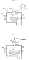
- Figs. 1 to 5 are cross sections to diagrammatically illustrate the constitution of a cleaning chamber 201, a sputtering film forming chamber 202, a plasma film forming chamber 203, an etching chamber 204 and a latent image forming chamber 205, respectively, that are used in carrying out the present invention.
- reference numeral 211 denotes a gas inlet provided above the cleaning chamber 201 so that a cleaning gas is fed into the cleaning chamber 201; 212, a sample holder that holds a sample 22 placed in the cleaning chamber 201; 213, an opposing electrode that opposes the sample holder 212; 214, an insulator for insulating the sample holder 212 from a vacuum chamber that constitutes the cleaning chamber 201; and 215, a high-frequency power source of 13.56 MHz and 200 W, which is electrically connected to the sample holder 212.
- Reference numeral 216 denotes a matching box for matching the both sides of the sample holder 212 and the high-frequency power source 215; and 217, a gate valve.
- reference numeral 221 denotes a gas inlet from which the sputtering gas is fed into the sputtering film forming chamber 202; 222, a sample holder that holds the sample 22 placed in the sputtering film forming chamber 202; 223, an opposing electrode provided opposingly to the sample holder 222 and to which a high-frequency electric power is applied; 224, an insulator for insulating the opposing electrode 223 from a vacuum chamber that constitutes the sputtering film forming chamber 202; 225, a high-frequency power source of 13.56 MHz and 500 W; 226, a matching box for matching the both sides of the sample holder 222 and the high-frequency power source 225; 227, a capacitor for insulating the
- reference numeral 231 denotes a gas inlet from which a deposition gas is fed into the plasma film forming chamber 203; 232, a sample holder that holds the sample 22 placed in the plasma film forming chamber 203; 223, an opposing electrode provided opposingly to the sample holder 232 and to which a high-frequency electric power is applied; 234, an insulator for insulating the opposing electrode 233 from a vacuum chamber that constitutes the plasma film forming chamber 203; 235, a high-frequency power source of 13.56 MHz and 350 W; 236, a matching box for matching the both sides of the sample holder 232 and the high-frequency power source 235; and 237, a gate valve.
- reference numeral 242 denotes a sample holder that holds the sample 22 placed in the etching chamber 204; 234, a microwave plasma gas exciting device for generating excited gas supplied to the etching chamber 204; 241, a gas inlet from which an etching gas is fed into the microwave plasma gas exciting device 243; 244, a transport pipe through which the excited gas generated in the microwave plasma gas exciting device 243 is transported to the etching chamber 204; and 245, a gate valve.
- reference numeral 251 denotes a gas inlet from which a modifying gas is fed into the latent image forming chamber 205; 252, a sample holder that holds the sample 22 placed in the latent image forming chamber 205; 253, a KrF excimer laser serving as a light source; 254, an illumination optical system for illuminating a mask 255 comprised of a quartz substrate (or a reticle) patterned with Cr; 256, a projection optical system for forming an image of the mask pattern on the surface of the sample 22; 257, a window through which the light having come out of the projection optical system 256 is led into the latent image forming chamber 205; and 258, a gate valve.
- the light source 253, the illumination optical system 254, the mask 255, the projection optical system 256 are provided above the latent image forming chamber 205.
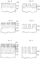
- Figs. 6A and 6B are diagrammatic cross sections to stepwise illustrate a procedure for forming an Al electrode pattern on a quartz substrate 261 according to the present example.
- Figs. 6C and 6D are cross sections to respectively show states in which the films shown in Figs. 6A and 6B have been etched.
- the quartz substrate 261 shown as the sample 22 in Figs. 1 to 5 , was placed on the sample holder 222 of the sputtering film forming chamber 202 shown in Fig. 2 . Subsequently, the inside of the sputtering film forming chamber 202 was evacuated to a pressure of 10 -7 Torr or less by means of a vacuum exhaust system (not shown). Ar gas was fed into the sputtering film forming chamber 202 from the gas inlet 221, and the vacuum exhaust system (not shown) was operated so as for the pressure in the sputtering film forming chamber 202 to be adjusted to 0.5 Torr.
- a current with a high-frequency of 13.56 MHz and 500 W was applied to the opposing electrode 223 while controlling the matching box 226, to generate plasma in the space between the sample holder 222 and the opposing electrode 223, to effect plasma decomposition of the gas fed therein, and to sputter an aluminum target attached to the opposing electrode 223 as a sputtering target, and thus, as shown in Fig. 6A , a film 262 to be etched, comprised of an Al film with a thickness of 3,000 ⁇ , was formed on the quartz substrate 261.
- this quartz substrate 261 was subjected to surface cleaning in the following way, in the cleaning chamber 201 shown in Fig.1 .
- the sample was placed on the sample holder 212, and the inside of the chamber was evacuated to a pressure of 10 -7 Torr or less by means of a vacuum exhaust system (not shown).
- a gas for cleaning the surface of the sample i.e., Ar gas in this instance, was fed at a flow rate of 50 sccm into the cleaning chamber 201, and the vacuum exhaust system (not shown) was operated so as for the pressure in the cleaning chamber 201 to be adjusted to 0.08 Torr.
- a current with a high-frequency of 13.56 MHz and 100 W was applied to the sample holder 212 while making adjustment of the matching box 216, to generate plasma in the space between the sample holder 212 and the opposing electrode 213. Since the sample holder 212 was insulated by a capacitor (not shown) in the direction of direct currents, a negative DC bias voltage of about -60 V was generated between the sample holder 212 and the opposing electrode 213 because of the difference in mobility between electrons and ions. Because of this voltage, Ar ions were accelerated and they collided against the surface of the film 262 to be etched, so that the stain present on the surface was physically removed by sputtering and thus a cleaned surface was obtained. The processing time was about 60 seconds.
- NO 2 gas was fed from the gas inlet 251 into the latent image forming chamber 205, and the vacuum exhaust system was operated so as for the inside pressure to be adjusted to 1 Torr.
- the laser light of 248 nm in wavelength radiated by means of the KrF excimer laser serving as the light source 253, the mask 255 was uniformly irradiated through the illumination optical system 254, and then an image of the pattern formed on the mask 255 was formed on the surface of the Al film through the window 257 by means of the projection optical system 256.
- quartz was used so that the laser light with an wavelength of 248 nm was transmitted without being absorbed.
- the quartz substrate 261 was again processed in the sputtering film forming chamber 202 shown in Fig. 2 under the same conditions to form on its surface an aluminum film with a thickness of 50 ⁇ as a film 264 to be etched. Then the surface thus processed was cleaned in the cleaning chamber 201 shown in Fig. 1 under the same conditions previously described. Thereafter, in the latent image forming chamber 205 shown in Fig. 5 , as a second protective film 265 an AlO x film with a thickness of 10 ⁇ was formed under the same conditions previously described, at the same position as the first protective film 263 as shown in Fig. 6B .
- the first protective film 263 and the second protective film 264 were 20 ⁇ in total thickness.
- the resulting sample was subjected to chemical dry etching in the following way in the etching chamber 204 shown in Fig.4 .
- the quartz substrate 261 was placed on the sample holder 242, and the inside of the etching chamber 204 was evacuated to a pressure of 10 -7 Torr or less by means of a vacuum exhaust system (not shown).
- Microwaves of 2.45 GHz and 700 W generated using a microwave generator (not shown) were supplied to the microwave plasma gas exciting device 243 to make the etching gas into plasma.
- the overall etching selection ratio in this instance, of the films 262 and 264 to be etched to the first and second protective films 263 and 265 was 150, and hence it was possible to form, after completion of etching, an Al electrode pattern with a sufficent height, comprised of the film 262 having been etched, as shown in Fig. 6D . It was possible to obtain a sufficient etching depth compared with the depth shown in Fig. 6c which was obtained by etching the film shown in Fig. 6A .
- Figs. 7A to 7C are diagrammatic cross sections to stepwise illustrate a fabrication procedure used when a pattern of an a-Si film, a semiconductor layer, is formed on an ITO-deposited quartz substrate 271 according to Example 2 of the present invention.
- Figs. 7D to 7F are diagrammatic cross sections to illustrate states wherein those shown in Figs. 7A to 7C have been etched, respectively.
- the quartz substrate 271 was placed on the sample holder 232 previously heated to 250°C with a heater (not shown) in the plasma film forming chamber 203 shown in Fig. 3 .
- the inside of the plasma film forming chamber 203 was evacuated to a pressure of 10 -7 Torr or less by means of a vacuum exhaust system (not shown), and the substrate was heated to a temperature of 250°C.
- SiH 4 and H 2 were fed at flow rates of 50 sccm and 500 sccm, respectively, into the plasma film forming chamber 203, and the vacuum exhaust system (not shown) was operated so as for the pressure in the plasma film forming chamber 203 to be adjusted to 0.5 Torr.
- a current with a high-frequency of 13.56 MHz and 50 W was applied to the opposing electrode 233 while controlling the matching box 236, to generate plasma in the space between the sample holder 232 and the opposing electrode 233, to effect plasma decomposition of the gas fed therein.
- an a-Si film with a thickness of 9,000 ⁇ was deposited as a film 272 to be etched, as shown in Fig. 7A .
- this quartz substrate 271 was subjected to surface cleaning in the same manner as in Example 1 , in the cleaning chamber 201 shown in Fig. 1.
- the substrate was again processed in the plasma film forming chamber 203 shown in Fig. 3 under the same conditions as previous ones to form on its surface an a-Si film with a thickness of 50 ⁇ . Then the surface of the sample was cleaned in the cleaning chamber 201 shown in Fig. 1 under the same conditions as those previously used. Thereafter, in the latent image forming chamber 205 shown in Fig. 5 , another layer SiO 2 film was formed under the same conditions as those previously described was formed at the same position as the first protective film 273 shown in Fig. 7A .
- the quartz substrate 271 was subjected to chemical dry etching for 150 seconds under the same conditions as those used in Example 1 , in the etching chamber 204 shown in Fig. 4 .
- the overall etching selection ratio in this instance, of the films 272, 274 and 276 to be etched to the first to third protective films 273, 275 and 277 was 300, and hence it was possible to form, after completion of etching, an etched pattern with the desired height as shown in Fig. 7F .
- Example 3 a process of forming an a-Si film pattern like that in Example 2 will be shown below.
- the films up to the second protective film 275 was formed in the same manner as in Example 2 . Thereafter, in the plasma film forming chamber 203 as shown in Fig. 3 , a 50 ⁇ thick n + -Si film was formed under the same conditions as in Example 3 except that H 2 -diluted 100 ppm PH 3 , SiH 4 and H 2 were fed from the gas inlet 231 at flow rates of 150 sccm, 5 sccm and 30 sccm, respectively. Thereafter, the surface of the film was cleaned under the same conditions as in Example 2 to form a surface-modified layer (thickness of protective film: 30 ⁇ ), followed by etching. As a result, it was possible to obtain an a-Si film with the desired pattern as shown in Fig. 7F .
- a plurality of the films to be etched, deposited on the substrate may be formed of different materials so long as they can be etched using the same etchant.
- the present invention which is constituted as described above has the following effects.
- Formation of a plurality of protective films can bring about a sufficiently large total layer thickness, and hence the fine processing with a sufficient etching depth can be applied.
- the substrate can be moved from the latent image forming chamber to the etching chamber through the gate valve. Hence, no dust can be adhered to the substrate surface, and the accuracy in the pattern formation can be improved.
- the latent image forming chamber is connected with the cleaning chamber similarly through the gate valve, so that the substrate is cleaned before the surface-modified layer is formed on the substrate. This can bring about a great effect.
Landscapes
- Physics & Mathematics (AREA)
- General Physics & Mathematics (AREA)
- Health & Medical Sciences (AREA)
- Chemical & Material Sciences (AREA)
- Engineering & Computer Science (AREA)
- Environmental & Geological Engineering (AREA)
- Public Health (AREA)
- Epidemiology (AREA)
- Chemical Kinetics & Catalysis (AREA)
- Toxicology (AREA)
- Life Sciences & Earth Sciences (AREA)
- Organic Chemistry (AREA)
- General Chemical & Material Sciences (AREA)
- Atmospheric Sciences (AREA)
- Optics & Photonics (AREA)
- Metallurgy (AREA)
- Mechanical Engineering (AREA)
- Materials Engineering (AREA)
- Computer Networks & Wireless Communication (AREA)
- Inorganic Chemistry (AREA)
- Drying Of Semiconductors (AREA)
- Finish Polishing, Edge Sharpening, And Grinding By Specific Grinding Devices (AREA)
- Electrical Discharge Machining, Electrochemical Machining, And Combined Machining (AREA)
- Internal Circuitry In Semiconductor Integrated Circuit Devices (AREA)
- Chemical Vapour Deposition (AREA)
- Electrodes Of Semiconductors (AREA)
Abstract
The present invention provides a processing method which comprises a first step of depositing on a substrate (271) a film to be etched (272); a second step of subjecting the film to be etched, to selective irradiation with light to form a protective film having a partially modified surface (273); and a third step of subjecting said film to be etched, to dry etching using said protective film as an etching mask. Said first step and said second step are continuously carried out plural times to respectively deposit on said substrate said film to be etched and said protective film in plurality (274,275,276,277), and thereafter said third step is carried out.
Description
- The present invention relates to a processing method and an apparatus usable for the method. More particularly it relates to a processing method that can apply the desired patterning to semiconductors, metals, insulators, etc., and an apparatus that can be used for such patterning.
- One of important techniques in the fabrication of semiconductor devices is photolithography. In the photolithography, a complicated and cumbersome process comprising the steps of resist coating, pattern exposure, development, etching, resist removing, etc. has been in wide use.
- In recent years, as typified by semiconductor memory devices, there is a rapid progress in providing devices with a larger capacity and their functions with a higher performance. With such a progress, circuit patterns are being made finer and also the structure of circuits is being more complicated. As for display devices such as liquid-crystal display devices and plasma-display devices, they are being made larger in size and device functions thereof are being made more complicated. Fabrication of these devices by the use of the above processes may result in an increase in cost because of the processes that may be made more complicated, and may bring about a decrease in yield because of an increase in generation of dust to cause an increase in cost as a whole.
- Thin-film devices are mainly fabricated by a process comprising the steps of forming on a substrate a thin film of a metal, a semiconductor, an insulator or the like, and finely processing the thin film to have the desired pattern. In recent years, as typified by semiconductor memory devices, there is a rapid progress in providing devices with a larger capacity and their functions with a higher performance. With such a progress, circuit patterns are being made finer and also the structure of circuits is being more complicated. As for display devices such as liquid-crystal display devices and plasma-display devices, they are being made larger in size and device functions thereof are being made more complicated. For this reason, film formation and also etching for applying fine processing, which had been carried out by a process making use of a solution, are now mainly carried out by what is called a dry process making use of plasma or excited gas in vacuum or in pressure-reduced gas. The photolithography commonly used for applying the desired fine processing, however, requires a complicated and cumbersome process comprising the steps of resist coating, pattern exposure, development, etching, resist removing, etc. Of these steps, the steps of resist coating, development and resist removing make use of solutions, and hence it is impossible for all the steps to be carried through a dry process. Accompanying these steps, the photolithography also requires a cleaning step or a drying step after the step of solution treatment, resulting in an increase in steps and making the process more complicated. The resist used in the above photolithography, when stripped, may come to be a source of dust, thus causing a decrease in yield and an increase in cost.
- As a method of carrying out fine processing without use of such a resist, there is a method of carrying out fine processing by a process comprising the steps of selectively irradiating the surface of a film to be processed, with light in a modifying gas to form a surface-modified layer having thereon a pattern structure, and dry-etching a surface-unmodified layer, using the surface-modified layer as a protective film. This process makes it possible to carry out fine processing wherein all the steps are carried through a dry process, without use of photolithography, and hence to promise a low cost and a high yield.
- On the other hand, in place of the above photolithography making use of a resist, a photoetching technique is proposed which can form a pattern by a process wherein the complicated process has been greatly simplified, as disclosed in Sekine, Okano and Horiike, Draft Collections of Lectures in the 5th Dry Processing Symposium, page 97 (1983). This paper reports a process in which a substrate comprising a polysilicon (poly-Si) deposited thereon is placed in a reaction chamber into which chlorine gas has been introduced and the Si substrate is selectively irradiated with ultraviolet light through a mask, whereupon only the part irradiated with the ultraviolet light is etched and a pattern is formed on the poly-Si film. Use of this process makes it possible to omit the steps of resist coating, development and resist removing, to simplify the process, to improve the yield and to greatly reduce the cost. Use thereof also may cause no damage due to ion irradiation, which has been questioned in conventional reactive ion etching, and hence enables damage-free etching.
- In this photoetching process, however, it is very difficult to perform fine processing faithful to a pattern because of the scattering or diffraction of light at the inside of processed grooves. In addition, in order to carry out perfect anisotropic etching, a side-wall protective film must be formed, and as a result this film may remain as a residue to have an ill influence on the device. In instances in which large-area display devices as exemplified by 14 inch liquid-crystal display devices are manufactured, the poly-Si is etched at a very low rate, which is 40 Å/min at most, as reported in the above Sekine et al.'s report. This is lower by the factor of about 2 figures than those in other etching processes. Moreover, under existing circumstances, the process can not reach the level of practical use at all even if an excimer laser having an output which is highest at present (about 100 W) is used as a light source, since the irradiation area is larger by the factor of ∼ 2 x 10⁴ times than the conventional one. In addition, there has been the problem that a substance produced as a result of etching reaction may be deposited on the window through which the ultraviolet light is shed and hence the window must be often cleaned.
- As stated above, a process has been proposed which is a method of carrying out fine processing by a process comprising the steps of selectively irradiating the surface of a film to be processed, with light in a modified gas to form a surface-modified layer having thereon a pattern structure, and dry-etching a surface-unmodified layer, using the surface-modified layer as a protective film (an etching mask). This process makes it possible to carry out fine processing without use of photolithography, and hence achieve an improvement in yield at a low cost. The process, however, often requires a long period of time or a strong light power at the time of the surface modification. If the processing is carried out for a short time or at a weak light power, the protective film formed by the surface modification can not be chemically strongly bonded or may be formed in an insufficient thickness, often bringing about an insufficient resistance of the protective film to give no desired etching depth.
- Also when a film is selectively deposited on the surface-modified layer or the surface-unmodified layer by utilizing a difference in properties such as electron donative properties between the surface-modified layer formed by surface modification by the above selective light irradiation and the surface-unmodified layer, the difference in properties such as electron donative properties can not be sufficient if the protective layer formed by the surface modification is not chemically strongly bonded or formed in an insufficient thickness, so that no satisfactory selectivity may be obtained in the subsequent deposition.
- In the method described above, aluminum is mainly used as a material for the electrodes or wiring of devices, where these electrodes and wiring have been conventionally formed by a method in which an aluminum film is deposited on the whole surface of a substrate and then etching is carried out to form the desired pattern. As a method of depositing the aluminum film, sputtering such as magnetron sputtering has been used. Since, however, the sputtering is commonly a physical deposition process which is based on the flying in vacuum, of particles sputtered from a target, the film may be formed in an extremely small thickness at step portions or on insulating film side walls, resulting in a disconnection in an extreme instance. Non-uniformity in layer thickness or disconnection may cause the problem that the reliability of LSI is seriously lowered.
- In order to solve the problems as discussed above, various types of CVD (chemical vapor deposition) processes are proposed. In such processes, a chemical reaction of a starting material gas is utilized in any form in the course of film formation. In the case of plasma CVD or photo-induced CVD, the starting material gas is decomposed in a gaseous phase, and an active species produced there further reacts on the substrate to cause film formation.
- Since in these CVD processes the reaction takes place in a gaseous phase, the surface can be well covered irrespective of any surface irregularities on the substrate, but on the other hand the carbon atoms contained in the starting gas molecules may be undesirably incorporated into the film. In particular, in the case of plasma CVD, there has been the problem that charged particles cause damage, what is called plasma damage, like the case of sputtering.
- In heat CVD, the reaction taking place mainly on the substrate surface causes a film to grow, and hence the surface can be well covered irrespective of any surface irregularities on the substrate. This can prevent disconnection at step portions or the like. This process is also free from the damage caused by charged particles that may be caused in plasma CVD or sputtering. Hence, the heat CVD has been studied from various approaches as a method of forming aluminum films. As a method of forming an aluminum film by commonly available heat CVD, a method is used in which an organic aluminum having been dispersed in a carrier gas is transported onto a heated substrate and gas molecules are thermally decomposed on the substrate to form a film. In an example disclosed, for example, in Journal of Electrochemical Society, Vol. 131, page 2175 (1984), triisobutyl aluminum [(i-C4H9)3Al] (hereinafter "TIBA") is used as the organic aluminum and film formation is carried out at a temperature of 260°C under a reaction tube pressure of 0.5 Torr to form a film of 3.4 µΩ·cm.
- When the TIBA is used, no continuous film can be obtained unless a pretreatment is applied such that TiCl4 is flowed before the film formation to activate the substrate surface so that nuclei can be formed. Including the instance where TiCl4 is used, there is commonly a disadvantage that use of the TIBA may bring about a poor surface flatness. Japanese Patent Application Laid-open No. 63-33569 discloses a method in which no TiCl4 is used and instead an organic aluminum is heated in the vicinity of a substrate to thereby form a film. In this instance, as clearly stated in the publication, it is necessary to provide a step of removing an oxide film naturally formed on the substrate surface. The publication also discloses that since the TIBA can be used alone, it is unnecessary to use a carrier gas other than TIBA but Ar gas may be used as the carrier gas. There, however, is no assumption as to the reaction of TIBA with other gas (e.g., H2) and there is no disclosure as to the use of hydrogen as the carrier gas. The publication also mentions trimethyl aluminum (TMA) besides TIBA, but has no specific disclosure as to the gases other than them. This is due to the fact that any use of any organic metals must be individually studied since, in general, chemical properties of organic metals greatly change depending on slight changes in organic substituents attached to metal elements.
- Electrochemical Society, Draft Collections for the 2nd Symposium, Japanese Branch, page 75 (July 7, 1989) discloses a method concerning the formation of aluminum films by double-wall CVD method. In this method, an apparatus is so designed that the gas temperature becomes higher than the substrate temperature by the use of TIBA. This method has the disadvantages not only that it is difficult to control the difference between the gas temperature and the temperature on the substrate surface but also that bombs and conveying pipes must be heated. This method also has the problems such that no uniform continuous film can be obtained unless the film is made thick to a certain extent, the film has a poor flatness and the selectivity can not be maintained for a long period of time.
- Etching of aluminum may bring about after-corrosion, i.e., the corrosion of aluminum that may be caused by HCl generated because of the use of a chlorine gas such as Cl2 or CCl4 as a result of reaction of Cl2 or its reaction product such as AlCl3 adhered during etching, with water remaining in the air or etching chamber. This corrosion is a great cause of the disconnection of wiring or electrodes.
- Meanwhile, besides these techniques, there is a method making use of photo-induced CVD, in which the surface of a substrate is selectively irradiated with light to cause photochemical reaction only on the irradiated surface so that a material can be selectively deposited thereon. Since, however, it is impossible to cause no reaction at all in the gaseous phase, the material may necessarily be deposited on the part other than the irradiated part. In addition, the photo-induced CVD commonly brings about slow deposition, where the rate of deposition is smaller by the factor of one figure than that of the heat CVD.
- As semiconductor devices are made more highly integrated and made to have a higher performance, attention is also drawn to CVD, etching, surface modification, cleaning, etc. which utilize light irradiation. This is because such a process enables low-temperature processing and gives less damage, as greatly characteristic of a photo-process, and also because spatially selective processing has become indispensable for the process of fabricating semiconductor devices. Incidentally, a common process making use of photo-processing includes;
- 1) a process in which the surface of a substrate is irradiated with light in a reactive gas atmosphere to cause excitation and decomposition of the reactive gas to bring several kinds of gases into reaction (i.e., gaseous phase reaction), whereby a deposit is formed on the surface or the surface is etched or cleaned; and
- 2) a process in which the surface of a substrate is heated by light irradiation to cause the surface to thermochemically react with a reactive gas or irradiated with light to cause the surface to photochemically react with a reactive gas (i.e., interface reaction), whereby a deposit is formed on the surface or the surface is etched or cleaned.
-
- The former process can be exemplified by a process in which the surface of a substrate is irradiated with a KrF excimer laser light in a gas atmosphere comprising SiH4 and O2, to cause SiH4 and O2 to react in the gaseous phase so that SiO2 is deposited on the substrate. In this method, however, the reaction product may scatter at random in the gaseous phase and hence there is basically no spatial selectivity. As for the latter process, it can be exemplified by a process in which the substrate is etched in a Cl2 gas atmosphere. Although no details of the reaction process have been elucidated in this method, it is presumed that the electrons excited on the surface irradiated with light are received by the chlorine atoms and incorporated into the Si substrate, in the state of which the reaction proceeds, and hence it is possible to cause the reaction only on the surface irradiated with light and therefor to effect spatially selective processing.
- Of the above conventional thin-film device processing methods described above, the methods making use of photolithography have the problems of a decrease in yield and an increase in cost. The method making use of the photoetching technique has the problem that it is impossible to perform fine processing faithful to a pattern because of the scattering or diffraction of light at the inside of processed grooves. In addition, in order to carry out perfect anisotropic etching, a side-wall protective film must be formed, and this film may remain as a residue to have an ill influence on the device. Moreover, the poly-Si is etched at a rate as low as about 40 Å/min, which is lower by the factor of 2 figures than those in other etching processes. In instances in which large-area display devices as exemplified by 14 inch liquid crystal display devices are manufactured, the irradiation area becomes larger by the factor of ∼ 2 x 10⁴ times than the experimental data, and hence the process can not reach the level of practical use at all even if an excimer laser with an output which is highest at present (about 100 W) is used as a light source. In addition, there has been the problem that, where the ultraviolet light having passed the mask is shed on the Si substrate through an ultraviolet irradiation window provided in the wall of the reaction chamber, a substance produced as a result of etching reaction may be deposited on this ultraviolet irradiation window and may absorb the ultraviolet light to cause a lowering of etching speed, and hence the ultraviolet irradiation window must be often cleaned with cumbersomeness.
- Of the above fine-processing methods used in thin-film devices, the method making use of photolithography requires use of a resist, which is stripped, and hence the method has been involved in the problem that the resist stripped comes out as dust and adheres to the surface of a substrate to cause a deterioration of the performance of devices and also to bring about a decrease in yield.
- In the method in which the dry etching is carried out without use of the photolithography, manufacture at a low cost and in a high yield can be achieved, but no sufficiently high etching selectivity can be attained between the protective film serving as a mask in etching and the film to which the fine processing is to be applied. Thus there is the problem that if the protective film formed by surface modification carried out once has a small thickness, the protective film serving as a mask in dry etching may disappear and hence the etching of the film to which the fine processing is to be applied can not be in a sufficient amount (or depth).
- As another problem, these photo-excitation processes discussed above leave some room for improvement for their better adaptation to semiconductor devices having been made more highly integrated and made to have a higher performance. One of the room of improvement is that a light-absorptive cross-sectional area or a light-reactive cross-sectional area is so small that the rate of processing is low. For example, in the photo-excitation etching of a silicon substrate, most papers report that the etching rate is approximately 100 to 2,000 Å/min (Research Reports XII on New Electronic Materials, Photo-excitation Processing Technique Research Report 1, Japan Electronic Industry Association, March 1986), which is an etching rate lower by the factor of about one figure than that in the conventional plasma etching. In infrared irradiation using a CO2 laser or the like, the thermochemical reaction caused by the heating of the substrate is mainly utilized, and hence images may be blurred because of the diffusion of heat. This has sometimes caused a problem when the substrate surface must be processed in a good selectivity.
- In the above photoetching, it is impossible to perform fine processing faithful to a pattern because of the scattering or diffraction of light at the inside of processed grooves. In addition, in order to carry out perfect anisotropic etching, a side-wall protective film must be formed, and this film may remain as a residue to have an ill influence on the device.
- In instances in which large-area display devices as exemplified by 14 inch liquid-crystal display devices are manufactured, the poly-Si is etched at a very low rate, which is 40 Å/min at most, as reported in the Sekine et al.'s report. This is lower by the factor of about 2 figures than those in other etching processes. The process can not reach the level of practical use at all even if an excimer laser having an irradiation area which is larger by the factor of at least 2 x 10⁴ times and having an output which is highest at present (about 100 W) is used as a light source. In addition, there has been the problem that a substance produced as a result of etching reaction may be deposited on the ultraviolet irradiation window through which the ultraviolet light is passed, to cause a lowering of the etching rate, and hence the window must be often cleaned.
- The present invention was made taking account of the above problems involved in the prior art. An object of the present invention is to materialize a processing method that can rapidly apply fine processing faithful to a pattern, and can improve the yield, and an apparatus that can be used for such a method.
- Another object of the present invention is to materialize a processing method that can form in a sufficiently large thickness the protective film serving as a mask in dry etching and thereby can give a sufficient amount of etching.
- Still another object of the present invention is to provide a method of, and an apparatus for, applying fine processing to semiconductor devices, that can accurately form a circuit pattern by the use of a simple process.
- A further object of the present invention is to solve the problems that when the devices are fabricated by photolithography, not only the process is complicated to cause an increase in cost but also the dust is generated or increases to bring about a decrease in yield and to cause an increase in cost as a whole.
- A still further object of the present invention is to propose a method capable of forming a protective film that can give a chemically well strong bond and have particles with a large diameter to have a strong etching resistance.
- A still further object of the present invention is to provide a photo-processing method that enables high-rate processing, and a processing apparatus to which such a processing method can be applied.
- A still further object of the present invention is to provide a photo-processing method that can process in an excellent selectivity the desired region on the substrate, and a processing apparatus to which such a processing method can be applied.
- A still further object is to provide a semiconductor fabrication method, and a semiconductor fabrication apparatus, that can form an electrode or wiring in a high selectivity and in a good yield, by the use of aluminum which is a good conductor or a metal mainly composed of aluminum, without use of any resist.
-
- Figs. 1 to 5 cross-sectionally illustrate the
constitution of a
cleaning chamber 201, a sputteringfilm forming chamber 202, a plasmafilm forming chamber 203, anetching chamber 204 and a latentimage forming chamber 205, respectively, that are used in carrying out the present invention. - Figs. 6A to 6D stepwise illustrate cross-sectionally a procedure for fabricating a device according to Example 1 of the present invention.
- Figs. 7A to 7F stepwise illustrate cross-sectionally a procedure for fabricating a device according to Example 2 of the present invention.
-
- An embodiment of the processing method of the present invention that can achieve the above objects comprises;
- a first step of depositing on a substrate a film to be etched;
- a second step of subjecting the film to be etched, to selective irradiation with light to form a protective film having a partially modified surface; and
- a third step of subjecting said film to be
etched, to dry etching using said protective film as
an etching mask;
wherein said first step and said second step are continuously carried out plural times to respectively deposit on said substrate said film to be etched and said protective film in plurality, and thereafter said third step is carried out. -
- According to this method, the protective film serving as an etching mask in dry etching is formed in plurality. The etching depth obtained by the etching corresponds to the total layer thickness of all the protective films, and hence controlling the number of the protective film to be formed enables control of the etching depth when the fine processing is applied.
- Examples of the present invention will be described below with reference to the accompanying drawings.
- Example 1 of the present invention will be described below with reference to the drawings.
- Figs. 1 to 5 are cross sections to diagrammatically illustrate the constitution of a
cleaning chamber 201, a sputteringfilm forming chamber 202, a plasmafilm forming chamber 203, anetching chamber 204 and a latentimage forming chamber 205, respectively, that are used in carrying out the present invention. - In Fig. 1 illustrating the
cleaning chamber 201,reference numeral 211 denotes a gas inlet provided above thecleaning chamber 201 so that a cleaning gas is fed into thecleaning chamber 201; 212, a sample holder that holds asample 22 placed in thecleaning chamber 201; 213, an opposing electrode that opposes thesample holder 212; 214, an insulator for insulating thesample holder 212 from a vacuum chamber that constitutes thecleaning chamber 201; and 215, a high-frequency power source of 13.56 MHz and 200 W, which is electrically connected to thesample holder 212.Reference numeral 216 denotes a matching box for matching the both sides of thesample holder 212 and the high-frequency power source 215; and 217, a gate valve. In Fig.2 illustrating the sputteringfilm forming chamber 202,reference numeral 221 denotes a gas inlet from which the sputtering gas is fed into the sputteringfilm forming chamber 202; 222, a sample holder that holds thesample 22 placed in the sputteringfilm forming chamber 202; 223, an opposing electrode provided opposingly to thesample holder 222 and to which a high-frequency electric power is applied; 224, an insulator for insulating the opposingelectrode 223 from a vacuum chamber that constitutes the sputteringfilm forming chamber 202; 225, a high-frequency power source of 13.56 MHz and 500 W; 226, a matching box for matching the both sides of thesample holder 222 and the high-frequency power source 225; 227, a capacitor for insulating the opposingelectrode 224 in the direction of direct currents; 228, a sputtering target; and 229, a gate valve. In Fig. 3 illustrating the plasmafilm forming chamber 203,reference numeral 231 denotes a gas inlet from which a deposition gas is fed into the plasmafilm forming chamber 203; 232, a sample holder that holds thesample 22 placed in the plasmafilm forming chamber 203; 223, an opposing electrode provided opposingly to thesample holder 232 and to which a high-frequency electric power is applied; 234, an insulator for insulating the opposingelectrode 233 from a vacuum chamber that constitutes the plasmafilm forming chamber 203; 235, a high-frequency power source of 13.56 MHz and 350 W; 236, a matching box for matching the both sides of thesample holder 232 and the high-frequency power source 235; and 237, a gate valve. In Fig. 4 illustrating theetching chamber 204,reference numeral 242 denotes a sample holder that holds thesample 22 placed in theetching chamber 204; 234, a microwave plasma gas exciting device for generating excited gas supplied to theetching chamber 204; 241, a gas inlet from which an etching gas is fed into the microwave plasma gasexciting device 243; 244, a transport pipe through which the excited gas generated in the microwave plasma gasexciting device 243 is transported to theetching chamber 204; and 245, a gate valve. - In Fig. 5 illustrating the latent
image forming chamber 205 in which surface modification is carried out,reference numeral 251 denotes a gas inlet from which a modifying gas is fed into the latentimage forming chamber 205; 252, a sample holder that holds thesample 22 placed in the latentimage forming chamber 205; 253, a KrF excimer laser serving as a light source; 254, an illumination optical system for illuminating amask 255 comprised of a quartz substrate (or a reticle) patterned with Cr; 256, a projection optical system for forming an image of the mask pattern on the surface of thesample 22; 257, a window through which the light having come out of the projectionoptical system 256 is led into the latentimage forming chamber 205; and 258, a gate valve. Of the above apparatus, thelight source 253, the illuminationoptical system 254, themask 255, the projectionoptical system 256 are provided above the latentimage forming chamber 205. - Figs. 6A and 6B are diagrammatic cross sections to stepwise illustrate a procedure for forming an Al electrode pattern on a
quartz substrate 261 according to the present example. Figs. 6C and 6D are cross sections to respectively show states in which the films shown in Figs. 6A and 6B have been etched. - The present example will be described with reference to Figs. 1 to 5 and Figs. 6A to 6D .
- The
quartz substrate 261, shown as thesample 22 in Figs. 1 to 5 , was placed on thesample holder 222 of the sputteringfilm forming chamber 202 shown in Fig. 2 . Subsequently, the inside of the sputteringfilm forming chamber 202 was evacuated to a pressure of 10-7 Torr or less by means of a vacuum exhaust system (not shown). Ar gas was fed into the sputteringfilm forming chamber 202 from thegas inlet 221, and the vacuum exhaust system (not shown) was operated so as for the pressure in the sputteringfilm forming chamber 202 to be adjusted to 0.5 Torr. A current with a high-frequency of 13.56 MHz and 500 W was applied to the opposingelectrode 223 while controlling thematching box 226, to generate plasma in the space between thesample holder 222 and the opposingelectrode 223, to effect plasma decomposition of the gas fed therein, and to sputter an aluminum target attached to the opposingelectrode 223 as a sputtering target, and thus, as shown in Fig. 6A , afilm 262 to be etched, comprised of an Al film with a thickness of 3,000 Å, was formed on thequartz substrate 261. - Subsequently, this
quartz substrate 261 was subjected to surface cleaning in the following way, in thecleaning chamber 201 shown in Fig.1 . The sample was placed on thesample holder 212, and the inside of the chamber was evacuated to a pressure of 10-7 Torr or less by means of a vacuum exhaust system (not shown). From thegas inlet 211, a gas for cleaning the surface of the sample, i.e., Ar gas in this instance, was fed at a flow rate of 50 sccm into thecleaning chamber 201, and the vacuum exhaust system (not shown) was operated so as for the pressure in thecleaning chamber 201 to be adjusted to 0.08 Torr. Next, a current with a high-frequency of 13.56 MHz and 100 W was applied to thesample holder 212 while making adjustment of thematching box 216, to generate plasma in the space between thesample holder 212 and the opposingelectrode 213. Since thesample holder 212 was insulated by a capacitor (not shown) in the direction of direct currents, a negative DC bias voltage of about -60 V was generated between thesample holder 212 and the opposingelectrode 213 because of the difference in mobility between electrons and ions. Because of this voltage, Ar ions were accelerated and they collided against the surface of thefilm 262 to be etched, so that the stain present on the surface was physically removed by sputtering and thus a cleaned surface was obtained. The processing time was about 60 seconds. - Next, in order to partially form the surface-modified layer on the surface of the
film 262 to be etched, selective irradiation with light in a modifying gas atmosphere was carried out in the latentimage forming chamber 205 shown in Fig. 5 . In this instance, an AlOx film that served as a protective film (an etching mask) in the etching carried out later was formed in the following way: Thequartz substrate 261 was placed on thesample holder 252, and the inside of the latentimage forming chamber 205 was evacuated to a pressure of 10-7 Torr or less by means of a vacuum exhaust system (not shown). NO2 gas was fed from thegas inlet 251 into the latentimage forming chamber 205, and the vacuum exhaust system was operated so as for the inside pressure to be adjusted to 1 Torr. Next, with the laser light of 248 nm in wavelength, radiated by means of the KrF excimer laser serving as thelight source 253, themask 255 was uniformly irradiated through the illuminationoptical system 254, and then an image of the pattern formed on themask 255 was formed on the surface of the Al film through thewindow 257 by means of the projectionoptical system 256. As a material for thewindow 257, quartz was used so that the laser light with an wavelength of 248 nm was transmitted without being absorbed. On the surface of thefilm 262 to be etched on which the mask image had been formed, the photochemical reaction of NO2 with Al took place only at the part irradiated with the light, so that upon exposure for 10 minutes a firstprotective film 263 comprised of AlOx with a thickness of 10 Å was partially (patternwise) formed on the surface of thefilm 262 to be etched, as shown in Fig. 6A . At the part not irradiated with the light, this reaction did not proceed, and finally a negative pattern of the mask was formed on the surface of thefilm 262 to be etched. In other words, Al was modified to AlOx and the latent image was formed. The KrF excimer laser was used here as thelight source 253. The same effect was also obtained when lamp light sources such as a xenon lamp and a high-pressure mercury lamp or ultraviolet lasers such as an ArF excimer laser, an XeCl excimer laser and an Ar laser were used. - Since the first
protective film 263 formed in this way did not have a sufficient layer thickness, thequartz substrate 261 was again processed in the sputteringfilm forming chamber 202 shown in Fig. 2 under the same conditions to form on its surface an aluminum film with a thickness of 50 Å as afilm 264 to be etched. Then the surface thus processed was cleaned in thecleaning chamber 201 shown in Fig. 1 under the same conditions previously described. Thereafter, in the latentimage forming chamber 205 shown in Fig. 5 , as a secondprotective film 265 an AlOx film with a thickness of 10 Å was formed under the same conditions previously described, at the same position as the firstprotective film 263 as shown in Fig. 6B . As a result, the firstprotective film 263 and the secondprotective film 264 were 20 Å in total thickness. Subsequently, the resulting sample was subjected to chemical dry etching in the following way in theetching chamber 204 shown in Fig.4 . Thequartz substrate 261 was placed on thesample holder 242, and the inside of theetching chamber 204 was evacuated to a pressure of 10-7 Torr or less by means of a vacuum exhaust system (not shown). A gas, Cl2 in this instance, for etching thefilms exciting device 243, and the vacuum exhaust system (not shown) was operated so as for the pressure in theetching chamber 204 to be adjusted to 0.2 Torr. Microwaves of 2.45 GHz and 700 W generated using a microwave generator (not shown) were supplied to the microwave plasma gasexciting device 243 to make the etching gas into plasma. Excited molecules Cl2 and Cl, thus excited by the plasma, were supplied for 120 seconds to the surface of thequartz substrate 261 through thetransport pipe 244 made of quartz, of 20 cm in whole length and 40 mm in inner diameter. - The overall etching selection ratio in this instance, of the
films protective films film 262 having been etched, as shown in Fig. 6D . It was possible to obtain a sufficient etching depth compared with the depth shown in Fig. 6c which was obtained by etching the film shown in Fig. 6A . - Figs. 7A to 7C are diagrammatic cross sections to stepwise illustrate a fabrication procedure used when a pattern of an a-Si film, a semiconductor layer, is formed on an ITO-deposited
quartz substrate 271 according to Example 2 of the present invention. Figs. 7D to 7F are diagrammatic cross sections to illustrate states wherein those shown in Figs. 7A to 7C have been etched, respectively. - This example will be described with reference to Figs. 1 , 3, 5 and 7 .
- The
quartz substrate 271 was placed on thesample holder 232 previously heated to 250°C with a heater (not shown) in the plasmafilm forming chamber 203 shown in Fig. 3 . The inside of the plasmafilm forming chamber 203 was evacuated to a pressure of 10-7 Torr or less by means of a vacuum exhaust system (not shown), and the substrate was heated to a temperature of 250°C. From thegas inlet 231, SiH4 and H2 were fed at flow rates of 50 sccm and 500 sccm, respectively, into the plasmafilm forming chamber 203, and the vacuum exhaust system (not shown) was operated so as for the pressure in the plasmafilm forming chamber 203 to be adjusted to 0.5 Torr. A current with a high-frequency of 13.56 MHz and 50 W was applied to the opposingelectrode 233 while controlling thematching box 236, to generate plasma in the space between thesample holder 232 and the opposingelectrode 233, to effect plasma decomposition of the gas fed therein. Thus an a-Si film with a thickness of 9,000 Å was deposited as afilm 272 to be etched, as shown in Fig. 7A . - Subsequently, this
quartz substrate 271 was subjected to surface cleaning in the same manner as in Example 1 , in thecleaning chamber 201 shown in Fig. 1. - Next, an SiO2 film that serves as a first protective film in the etching carried out later was formed in the same way as in Example 1, in the latent
image forming chamber 205 shown in Fig. 5 . As a result, the photochemical reaction of NO2 with Si took place only at the part irradiated with the light, so that upon exposure for 10 minutes a firstprotective film 273 comprised of SiO2 with a thickness of 10 Å was patternwise formed on the surface of thefilm 272 to be etched, as shown in Fig. 7A . At the part not irradiated with the light, this reaction did not proceed, and finally a negative pattern of the mask was formed on the surface of thefilm 272 to be etched. In other words, a-Si was modified to SiO2 to form a latent image. - Since the first
protective film 273 formed in this way did not have a sufficient layer thickness compared with the thickness of thefilm 272 to be etched, the substrate was again processed in the plasmafilm forming chamber 203 shown in Fig. 3 under the same conditions as previous ones to form on its surface an a-Si film with a thickness of 50 Å. Then the surface of the sample was cleaned in thecleaning chamber 201 shown in Fig. 1 under the same conditions as those previously used. Thereafter, in the latentimage forming chamber 205 shown in Fig. 5 , another layer SiO2 film was formed under the same conditions as those previously described was formed at the same position as the firstprotective film 273 shown in Fig. 7A . A series of these steps were carried out twice to formfilms protective films - Subsequently, the
quartz substrate 271 was subjected to chemical dry etching for 150 seconds under the same conditions as those used in Example 1 , in theetching chamber 204 shown in Fig. 4 . The overall etching selection ratio in this instance, of thefilms protective films - As Example 3 , a process of forming an a-Si film pattern like that in Example 2 will be shown below.
- The films up to the second protective film 275 (see Fig. 7B ) was formed in the same manner as in Example 2 . Thereafter, in the plasma
film forming chamber 203 as shown in Fig. 3 , a 50 Å thick n+-Si film was formed under the same conditions as in Example 3 except that H2-diluted 100 ppm PH3, SiH4 and H2 were fed from thegas inlet 231 at flow rates of 150 sccm, 5 sccm and 30 sccm, respectively. Thereafter, the surface of the film was cleaned under the same conditions as in Example 2 to form a surface-modified layer (thickness of protective film: 30 Å), followed by etching. As a result, it was possible to obtain an a-Si film with the desired pattern as shown in Fig. 7F . - Thus, a plurality of the films to be etched, deposited on the substrate may be formed of different materials so long as they can be etched using the same etchant.
- The present invention, which is constituted as described above has the following effects.
- It is possible to prevent deterioration of devices and adhesion of dust, and hence the yield can also be improved in addition to the above effect.
- Formation of a plurality of protective films can bring about a sufficiently large total layer thickness, and hence the fine processing with a sufficient etching depth can be applied.
- According to the apparatus for fine-processing semiconductor devices, the substrate can be moved from the latent image forming chamber to the etching chamber through the gate valve. Hence, no dust can be adhered to the substrate surface, and the accuracy in the pattern formation can be improved. In addition, the latent image forming chamber is connected with the cleaning chamber similarly through the gate valve, so that the substrate is cleaned before the surface-modified layer is formed on the substrate. This can bring about a great effect.
- Needless to say, the respective processing methods and apparatus described giving examples can be used in combination within the purport of the present invention, and also can be modified within the purport of the present invention.
Claims (1)
- A processing method comprising;a first step of depositing on a substrate a film to be etched;a second step of subjecting the film to be etched, to selective irradiation with light to form a protective film having a partially modified surface; anda third step of subjecting said film to be etched, to dry etching using said protective film as an etching mask;
wherein said first step and said second step are continuously carried out plural times to respectively deposit on said substrate said film to be etched and said protective film in plurality, and thereafter said third step is carried out.
Applications Claiming Priority (17)
| Application Number | Priority Date | Filing Date | Title |
|---|---|---|---|
| JP2254196A JP2672185B2 (en) | 1990-09-26 | 1990-09-26 | Thin film element processing method and apparatus |
| JP254196/90 | 1990-09-26 | ||
| JP255148/90 | 1990-09-27 | ||
| JP2255148A JP2622188B2 (en) | 1990-09-27 | 1990-09-27 | Fine processing method of thin film device |
| JP261670/90 | 1990-09-29 | ||
| JP2261670A JP2840419B2 (en) | 1990-09-29 | 1990-09-29 | Light treatment method and light treatment device |
| JP26646190A JPH04144135A (en) | 1990-10-05 | 1990-10-05 | Manufacturing method and equipment for semiconductor devices |
| JP266461/90 | 1990-10-05 | ||
| JP314953/90 | 1990-11-19 | ||
| JP2314953A JP2667930B2 (en) | 1990-11-19 | 1990-11-19 | Fine processing method and device |
| JP2313589A JP2709188B2 (en) | 1990-11-19 | 1990-11-19 | Semiconductor device fine processing method and apparatus |
| JP314951/90 | 1990-11-19 | ||
| JP2314954A JP2756364B2 (en) | 1990-11-19 | 1990-11-19 | Optical surface treatment method and treatment device |
| JP314954/90 | 1990-11-19 | ||
| JP313589/90 | 1990-11-19 | ||
| JP2314951A JP2670465B2 (en) | 1990-11-19 | 1990-11-19 | Fine processing method |
| EP91116309A EP0477890B1 (en) | 1990-09-26 | 1991-09-25 | Processing method and apparatus |
Related Parent Applications (1)
| Application Number | Title | Priority Date | Filing Date |
|---|---|---|---|
| EP91116309A Division EP0477890B1 (en) | 1990-09-26 | 1991-09-25 | Processing method and apparatus |
Publications (1)
| Publication Number | Publication Date |
|---|---|
| EP0909988A1 true EP0909988A1 (en) | 1999-04-21 |
Family
ID=27573548
Family Applications (8)
| Application Number | Title | Priority Date | Filing Date |
|---|---|---|---|
| EP98124751A Withdrawn EP0908781A3 (en) | 1990-09-26 | 1991-09-25 | Photolithographic processing method and apparatus |
| EP98124748A Withdrawn EP0909986A1 (en) | 1990-09-26 | 1991-09-25 | Photolithographic processing method and apparatus |
| EP98124749A Withdrawn EP0909987A1 (en) | 1990-09-26 | 1991-09-25 | Photolithographic processing method and apparatus |
| EP98124755A Withdrawn EP0909989A1 (en) | 1990-09-26 | 1991-09-25 | Photolithographic processing method and apparatus |
| EP98124753A Withdrawn EP0909988A1 (en) | 1990-09-26 | 1991-09-25 | Photolithographic processing method |
| EP98124750A Withdrawn EP0909985A1 (en) | 1990-09-26 | 1991-09-25 | Photolithographic processing method and apparatus |
| EP91116309A Expired - Lifetime EP0477890B1 (en) | 1990-09-26 | 1991-09-25 | Processing method and apparatus |
| EP98124754A Withdrawn EP0908782A1 (en) | 1990-09-26 | 1991-09-25 | Photolithographic processing method |
Family Applications Before (4)
| Application Number | Title | Priority Date | Filing Date |
|---|---|---|---|
| EP98124751A Withdrawn EP0908781A3 (en) | 1990-09-26 | 1991-09-25 | Photolithographic processing method and apparatus |
| EP98124748A Withdrawn EP0909986A1 (en) | 1990-09-26 | 1991-09-25 | Photolithographic processing method and apparatus |
| EP98124749A Withdrawn EP0909987A1 (en) | 1990-09-26 | 1991-09-25 | Photolithographic processing method and apparatus |
| EP98124755A Withdrawn EP0909989A1 (en) | 1990-09-26 | 1991-09-25 | Photolithographic processing method and apparatus |
Family Applications After (3)
| Application Number | Title | Priority Date | Filing Date |
|---|---|---|---|
| EP98124750A Withdrawn EP0909985A1 (en) | 1990-09-26 | 1991-09-25 | Photolithographic processing method and apparatus |
| EP91116309A Expired - Lifetime EP0477890B1 (en) | 1990-09-26 | 1991-09-25 | Processing method and apparatus |
| EP98124754A Withdrawn EP0908782A1 (en) | 1990-09-26 | 1991-09-25 | Photolithographic processing method |
Country Status (4)
| Country | Link |
|---|---|
| US (4) | US5962194A (en) |
| EP (8) | EP0908781A3 (en) |
| AT (1) | ATE200829T1 (en) |
| DE (1) | DE69132587T2 (en) |
Families Citing this family (40)
| Publication number | Priority date | Publication date | Assignee | Title |
|---|---|---|---|---|
| IL119246A (en) * | 1996-09-12 | 2000-10-31 | Oramir Semiconductor Ltd | Laser removal of foreign materials from surfaces |
| US6107206A (en) * | 1998-09-14 | 2000-08-22 | Taiwan Semiconductor Manufacturing Company | Method for etching shallow trenches in a semiconductor body |
| US6727980B2 (en) | 1998-09-17 | 2004-04-27 | Nikon Corporation | Apparatus and method for pattern exposure and method for adjusting the apparatus |
| US6192897B1 (en) * | 1999-01-27 | 2001-02-27 | Euv Llc | Apparatus and method for in-situ cleaning of resist outgassing windows |
| US6762412B1 (en) * | 1999-05-10 | 2004-07-13 | Nikon Corporation | Optical apparatus, exposure apparatus using the same, and gas introduction method |
| CN1315822A (en) * | 2000-03-30 | 2001-10-03 | 日本胜利株式会社 | Film resistance element for printed circuit board and forming method thereof |
| JP4286439B2 (en) * | 2000-08-11 | 2009-07-01 | 富士通マイクロエレクトロニクス株式会社 | Manufacturing method of semiconductor device |
| KR100408137B1 (en) * | 2001-11-26 | 2003-12-06 | 학교법인 성균관대학 | Layer-by-layer etching apparatus using neutral beam and method of etching using the same |
| US6781126B2 (en) * | 2002-02-04 | 2004-08-24 | Applied Materials, Inc. | Auger-based thin film metrology |
| US20040007733A1 (en) * | 2002-06-26 | 2004-01-15 | Macronix International Co., Ltd. | Floating gate memory cell and forming method |
| KR100585472B1 (en) * | 2002-09-30 | 2006-06-07 | 에이에스엠엘 네델란즈 비.브이. | Lithographic Apparatus and Device Manufacturing Method |
| EP1403715A3 (en) * | 2002-09-30 | 2006-01-18 | ASML Netherlands B.V. | Lithographic apparatus and device manufacturing method |
| US7022615B2 (en) * | 2002-11-26 | 2006-04-04 | Matsushita Electric Industrial Co., Ltd. | Plasma processing method |
| JP2004221545A (en) * | 2002-12-26 | 2004-08-05 | Tokyo Electron Ltd | Plasma etching method |
| WO2004079450A1 (en) * | 2003-03-06 | 2004-09-16 | Yissum Research Development Company Of The Hebrew University Of Jerusalem | Method for manufacturing a patterned structure |
| US6872972B2 (en) * | 2003-07-16 | 2005-03-29 | Macronix International Co., Ltd. | Method for forming silicon film with changing grain size by thermal process |
| JP3655915B2 (en) * | 2003-09-08 | 2005-06-02 | Fcm株式会社 | Conductive sheet and product containing the same |
| WO2005019493A2 (en) * | 2003-08-11 | 2005-03-03 | Honeywell International Inc. | Target/backing plate constructions, and methods of forming them |
| US20050221586A1 (en) * | 2003-12-18 | 2005-10-06 | Mulligan Rose A | Methods and apparatus for laser dicing |
| JP5102492B2 (en) * | 2003-12-19 | 2012-12-19 | カール・ツァイス・エスエムティー・ゲーエムベーハー | Objective lens for microlithography projection with crystal elements |
| US7151883B2 (en) * | 2004-10-08 | 2006-12-19 | Hewlett-Packard Development Company, L.P. | Photonic crystal device and methods |
| JP5080009B2 (en) | 2005-03-22 | 2012-11-21 | 日立ビアメカニクス株式会社 | Exposure method |
| JP4599342B2 (en) * | 2005-12-27 | 2010-12-15 | エーエスエムエル ネザーランズ ビー.ブイ. | Optical apparatus, lithographic apparatus, and device manufacturing method |
| US20090227093A1 (en) * | 2006-02-17 | 2009-09-10 | Cornell Research Foundation, Inc | Patterning During Film Growth |
| US7449414B2 (en) * | 2006-08-07 | 2008-11-11 | Tokyo Electron Limited | Method of treating a mask layer prior to performing an etching process |
| US20080073596A1 (en) * | 2006-08-24 | 2008-03-27 | Asml Netherlands B.V. | Lithographic apparatus and method |
| JP2008251913A (en) * | 2007-03-30 | 2008-10-16 | Hoya Candeo Optronics株式会社 | Ultraviolet resistant material, sealing member, buffer member, light shielding member, light source device, and processing device using the same |
| JP4969304B2 (en) * | 2007-04-20 | 2012-07-04 | 東京エレクトロン株式会社 | Heat treatment plate temperature setting method, heat treatment plate temperature setting device, and computer-readable storage medium |
| US8013300B2 (en) * | 2008-06-20 | 2011-09-06 | Carl Zeiss Nts, Llc | Sample decontamination |
| EP2144117A1 (en) * | 2008-07-11 | 2010-01-13 | The Provost, Fellows and Scholars of the College of the Holy and Undivided Trinity of Queen Elizabeth near Dublin | Process and system for fabrication of patterns on a surface |
| US8536056B2 (en) * | 2011-08-22 | 2013-09-17 | Nanya Technology Corporation | Method of forming conductive pattern |
| WO2016099755A1 (en) * | 2014-12-15 | 2016-06-23 | Applied Materials, Inc. | Ultra-thin dielectric diffusion barrier and etch stop layer for advanced interconnect applications |
| CN104505334B (en) * | 2014-12-16 | 2017-10-24 | 桂林电子科技大学 | It is a kind of that the method for making Thinfilm pattern is heated by laser |
| US9613808B1 (en) * | 2016-01-19 | 2017-04-04 | United Microelectronics Corp. | Method of forming multilayer hard mask with treatment for removing impurities and forming dangling bonds |
| US10872760B2 (en) * | 2016-07-26 | 2020-12-22 | Taiwan Semiconductor Manufacturing Co., Ltd. | Cluster tool and manufacuturing method of semiconductor structure using the same |
| CN107799407B (en) * | 2016-08-29 | 2020-07-17 | 中国科学院苏州纳米技术与纳米仿生研究所 | Method for fabricating groove gate of transistor and high-power radio frequency device |
| JP6500874B2 (en) * | 2016-10-21 | 2019-04-17 | 株式会社豊田中央研究所 | Etching apparatus used for photoelectrochemical etching of semiconductor substrates |
| EP3606293B1 (en) * | 2017-03-31 | 2022-09-07 | Fuji Corporation | Plasma generation device |
| CN108735584B (en) * | 2018-05-29 | 2021-03-23 | 江苏永鼎股份有限公司 | A semiconductor chip production process |
| EP3875633A1 (en) * | 2020-03-03 | 2021-09-08 | Stichting Nederlandse Wetenschappelijk Onderzoek Instituten | Method and apparatus for forming a patterned layer of material |
Citations (2)
| Publication number | Priority date | Publication date | Assignee | Title |
|---|---|---|---|---|
| JPS61258433A (en) * | 1985-05-13 | 1986-11-15 | Hitachi Ltd | Etching process |
| EP0400791A2 (en) * | 1989-04-10 | 1990-12-05 | AT&T Corp. | Electronic device manufacture involving a pattern delineation step |
Family Cites Families (36)
| Publication number | Priority date | Publication date | Assignee | Title |
|---|---|---|---|---|
| US3326717A (en) * | 1962-12-10 | 1967-06-20 | Ibm | Circuit fabrication |
| US4845529A (en) * | 1987-12-18 | 1989-07-04 | Thomas W. Secrest | Storage apparatus comprising a plurality of layers |
| US4324854A (en) * | 1980-03-03 | 1982-04-13 | California Institute Of Technology | Deposition of metal films and clusters by reactions of compounds with low energy electrons on surfaces |
| JPS56164523A (en) * | 1980-05-21 | 1981-12-17 | Hitachi Ltd | Vapor phase growth of semiconductor |
| US4579750A (en) * | 1980-07-07 | 1986-04-01 | Massachusetts Institute Of Technology | Laser heated CVD process |
| US4361461A (en) * | 1981-03-13 | 1982-11-30 | Bell Telephone Laboratories, Incorporated | Hydrogen etching of semiconductors and oxides |
| JPS57208142A (en) * | 1981-06-17 | 1982-12-21 | Toshiba Corp | Method for forming fine pattern |
| JPS5839779A (en) * | 1981-09-01 | 1983-03-08 | Matsushita Electric Ind Co Ltd | Photo engraving method |
| JPS59161038A (en) * | 1983-03-04 | 1984-09-11 | Hitachi Ltd | Pattern forming process |
| JPS59194440A (en) * | 1983-04-18 | 1984-11-05 | Mitsubishi Electric Corp | Pattern forming apparatus |
| FR2548218B1 (en) * | 1983-06-29 | 1987-03-06 | Pauleau Yves | METHOD FOR DEPOSITING THIN FILMS BY GAS PHASE CHEMICAL REACTION USING TWO DIFFERENT RADIATIONS |
| US4470871A (en) * | 1983-12-27 | 1984-09-11 | Rca Corporation | Preparation of organic layers for oxygen etching |
| JPH07107190B2 (en) * | 1984-03-30 | 1995-11-15 | キヤノン株式会社 | Photochemical vapor deposition method |
| JPS60211074A (en) * | 1984-04-05 | 1985-10-23 | Fuji Electric Corp Res & Dev Ltd | Formation of electrically conductive film pattern |
| JPS6129129A (en) * | 1984-07-19 | 1986-02-10 | Toshiba Corp | Dry etching method |
| JPS6167228A (en) * | 1984-09-10 | 1986-04-07 | Hitachi Ltd | Fine pattern forming method |
| JPS61104614A (en) * | 1984-10-29 | 1986-05-22 | Canon Inc | Formation of deposited film |
| US4810601A (en) * | 1984-12-07 | 1989-03-07 | International Business Machines Corporation | Top imaged resists |
| JPS61187237A (en) * | 1985-02-14 | 1986-08-20 | Toshiba Corp | Formation of pattern |
| US4685976A (en) * | 1985-04-10 | 1987-08-11 | Eaton Corporation | Multi-layer semiconductor processing with scavenging between layers by excimer laser |
| US4612085A (en) * | 1985-04-10 | 1986-09-16 | Texas Instruments Incorporated | Photochemical patterning |
| US4670063A (en) * | 1985-04-10 | 1987-06-02 | Eaton Corporation | Semiconductor processing technique with differentially fluxed radiation at incremental thicknesses |
| US4619894A (en) * | 1985-04-12 | 1986-10-28 | Massachusetts Institute Of Technology | Solid-transformation thermal resist |
| JPS61278146A (en) * | 1985-06-03 | 1986-12-09 | Toshiba Corp | Optical treatment method |
| US4931380A (en) * | 1985-07-18 | 1990-06-05 | Microsi, Inc. | Pre-exposure method for increased sensitivity in high contrast resist development of positive working diazo ketone photoresist |
| JPS62262433A (en) * | 1986-05-09 | 1987-11-14 | Hitachi Ltd | Surface treating method |
| JP2559030B2 (en) * | 1986-07-25 | 1996-11-27 | 日本電信電話株式会社 | Method for manufacturing metal thin film |
| JPH0774452B2 (en) * | 1986-11-27 | 1995-08-09 | キヤノン株式会社 | Method for forming functional deposited film by photochemical vapor deposition |
| JPS63165845A (en) * | 1986-12-26 | 1988-07-09 | Toshiba Corp | Pattern forming method |
| US5062149A (en) * | 1987-10-23 | 1991-10-29 | General Dynamics Corporation | Millimeter wave device and method of making |
| US4908226A (en) * | 1988-05-23 | 1990-03-13 | Hughes Aircraft Company | Selective area nucleation and growth method for metal chemical vapor deposition using focused ion beams |
| US5041361A (en) * | 1988-08-08 | 1991-08-20 | Midwest Research Institute | Oxygen ion-beam microlithography |
| JPH02265240A (en) * | 1989-04-06 | 1990-10-30 | Matsushita Electron Corp | Dry etching apparatus |
| DE3938669A1 (en) * | 1989-11-21 | 1991-05-23 | Max Planck Gesellschaft | METHOD FOR BACTERIZING A SURFACE TO BE METALLIZED |
| DE69132523D1 (en) * | 1990-05-09 | 2001-03-08 | Canon Kk | Generation of patterns and manufacturing processes for semiconductor devices with this pattern |
| US5503961A (en) * | 1994-11-02 | 1996-04-02 | International Business Machines Corporation | Process for forming multilayer lift-off structures |
-
1991
- 1991-09-25 EP EP98124751A patent/EP0908781A3/en not_active Withdrawn
- 1991-09-25 EP EP98124748A patent/EP0909986A1/en not_active Withdrawn
- 1991-09-25 EP EP98124749A patent/EP0909987A1/en not_active Withdrawn
- 1991-09-25 DE DE69132587T patent/DE69132587T2/en not_active Expired - Fee Related
- 1991-09-25 AT AT91116309T patent/ATE200829T1/en not_active IP Right Cessation
- 1991-09-25 EP EP98124755A patent/EP0909989A1/en not_active Withdrawn
- 1991-09-25 EP EP98124753A patent/EP0909988A1/en not_active Withdrawn
- 1991-09-25 EP EP98124750A patent/EP0909985A1/en not_active Withdrawn
- 1991-09-25 EP EP91116309A patent/EP0477890B1/en not_active Expired - Lifetime
- 1991-09-25 EP EP98124754A patent/EP0908782A1/en not_active Withdrawn
-
1994
- 1994-05-31 US US08/251,666 patent/US5962194A/en not_active Expired - Fee Related
-
1995
- 1995-04-25 US US08/429,287 patent/US5863706A/en not_active Expired - Fee Related
- 1995-04-25 US US08/429,288 patent/US6025115A/en not_active Expired - Fee Related
- 1995-04-25 US US08/429,289 patent/US5981001A/en not_active Expired - Fee Related
Patent Citations (2)
| Publication number | Priority date | Publication date | Assignee | Title |
|---|---|---|---|---|
| JPS61258433A (en) * | 1985-05-13 | 1986-11-15 | Hitachi Ltd | Etching process |
| EP0400791A2 (en) * | 1989-04-10 | 1990-12-05 | AT&T Corp. | Electronic device manufacture involving a pattern delineation step |
Non-Patent Citations (2)
| Title |
|---|
| "REGISTERABLE MULTILAYER MASK FABRICATION TECHNIQUE", IBM TECHNICAL DISCLOSURE BULLETIN, vol. 27, no. 1B, June 1984 (1984-06-01), XP002015431 * |
| PATENT ABSTRACTS OF JAPAN vol. 011, no. 110 (E - 496) 7 April 1987 (1987-04-07) * |
Also Published As
| Publication number | Publication date |
|---|---|
| US5981001A (en) | 1999-11-09 |
| DE69132587D1 (en) | 2001-05-31 |
| EP0909985A1 (en) | 1999-04-21 |
| EP0908781A3 (en) | 1999-04-21 |
| ATE200829T1 (en) | 2001-05-15 |
| US6025115A (en) | 2000-02-15 |
| US5962194A (en) | 1999-10-05 |
| EP0909987A1 (en) | 1999-04-21 |
| EP0908782A1 (en) | 1999-04-14 |
| EP0477890A3 (en) | 1996-12-18 |
| EP0477890A2 (en) | 1992-04-01 |
| EP0908781A2 (en) | 1999-04-14 |
| EP0909989A1 (en) | 1999-04-21 |
| EP0477890B1 (en) | 2001-04-25 |
| US5863706A (en) | 1999-01-26 |
| DE69132587T2 (en) | 2001-09-06 |
| EP0909986A1 (en) | 1999-04-21 |
Similar Documents
| Publication | Publication Date | Title |
|---|---|---|
| EP0909988A1 (en) | Photolithographic processing method | |
| US5344522A (en) | Pattern forming process and process for preparing semiconductor device utilizing said pattern forming process | |
| US5380397A (en) | Method of treating samples | |
| CN101312126B (en) | Method of forming amorphous carbon film and method of manufacturing semiconductor device using same | |
| JP3283477B2 (en) | Dry etching method and semiconductor device manufacturing method | |
| JP3048749B2 (en) | Thin film formation method | |
| US5714306A (en) | Processing method and apparatus | |
| US5409802A (en) | Method and apparatus for fine processing | |
| JP2849458B2 (en) | Semiconductor device manufacturing method and manufacturing apparatus | |
| EP0466320B1 (en) | Process for preparing a semiconductor device including the selective deposition of a metal | |
| US20250130500A1 (en) | Methods for forming euv resist underlayer | |
| JP2672185B2 (en) | Thin film element processing method and apparatus | |
| JP2622188B2 (en) | Fine processing method of thin film device | |
| JPH04343423A (en) | Damage-free dry etching method | |
| JP3110472B2 (en) | Selective metal deposition method | |
| JPH04188620A (en) | Microfabrication method and device | |
| JPH07307277A (en) | Method for forming antireflection film and method for forming fine pattern | |
| JPH0621023A (en) | Manufacture of thin film device |
Legal Events
| Date | Code | Title | Description |
|---|---|---|---|
| PUAI | Public reference made under article 153(3) epc to a published international application that has entered the european phase |
Free format text: ORIGINAL CODE: 0009012 |
|
| AC | Divisional application: reference to earlier application |
Ref document number: 477890 Country of ref document: EP |
|
| AK | Designated contracting states |
Kind code of ref document: A1 Designated state(s): AT BE CH DE DK ES FR GB GR IT LI LU NL SE |
|
| 17P | Request for examination filed |
Effective date: 19990914 |
|
| 17Q | First examination report despatched |
Effective date: 20000317 |
|
| STAA | Information on the status of an ep patent application or granted ep patent |
Free format text: STATUS: THE APPLICATION IS DEEMED TO BE WITHDRAWN |
|
| 18D | Application deemed to be withdrawn |
Effective date: 20020108 |