EP0909976B1 - Anzeigevorrichtung mit einer bilderzeugenden Tafel und einer Beleuchtungsvorrichtung an deren Rückseite - Google Patents
Anzeigevorrichtung mit einer bilderzeugenden Tafel und einer Beleuchtungsvorrichtung an deren Rückseite Download PDFInfo
- Publication number
- EP0909976B1 EP0909976B1 EP97402424.2A EP97402424A EP0909976B1 EP 0909976 B1 EP0909976 B1 EP 0909976B1 EP 97402424 A EP97402424 A EP 97402424A EP 0909976 B1 EP0909976 B1 EP 0909976B1
- Authority
- EP
- European Patent Office
- Prior art keywords
- photo
- display device
- panel
- transistor
- switching
- Prior art date
- Legal status (The legal status is an assumption and is not a legal conclusion. Google has not performed a legal analysis and makes no representation as to the accuracy of the status listed.)
- Expired - Lifetime
Links
- 238000005286 illumination Methods 0.000 title claims description 14
- 239000004973 liquid crystal related substance Substances 0.000 claims description 15
- 230000003287 optical effect Effects 0.000 claims description 9
- 238000001514 detection method Methods 0.000 claims description 5
- 210000004027 cell Anatomy 0.000 description 11
- 210000002858 crystal cell Anatomy 0.000 description 5
- 239000004020 conductor Substances 0.000 description 2
- 230000007423 decrease Effects 0.000 description 2
- 230000003068 static effect Effects 0.000 description 1
Images
Classifications
-
- G—PHYSICS
- G02—OPTICS
- G02F—OPTICAL DEVICES OR ARRANGEMENTS FOR THE CONTROL OF LIGHT BY MODIFICATION OF THE OPTICAL PROPERTIES OF THE MEDIA OF THE ELEMENTS INVOLVED THEREIN; NON-LINEAR OPTICS; FREQUENCY-CHANGING OF LIGHT; OPTICAL LOGIC ELEMENTS; OPTICAL ANALOGUE/DIGITAL CONVERTERS
- G02F1/00—Devices or arrangements for the control of the intensity, colour, phase, polarisation or direction of light arriving from an independent light source, e.g. switching, gating or modulating; Non-linear optics
- G02F1/01—Devices or arrangements for the control of the intensity, colour, phase, polarisation or direction of light arriving from an independent light source, e.g. switching, gating or modulating; Non-linear optics for the control of the intensity, phase, polarisation or colour
- G02F1/13—Devices or arrangements for the control of the intensity, colour, phase, polarisation or direction of light arriving from an independent light source, e.g. switching, gating or modulating; Non-linear optics for the control of the intensity, phase, polarisation or colour based on liquid crystals, e.g. single liquid crystal display cells
- G02F1/133—Constructional arrangements; Operation of liquid crystal cells; Circuit arrangements
- G02F1/136—Liquid crystal cells structurally associated with a semi-conducting layer or substrate, e.g. cells forming part of an integrated circuit
- G02F1/1362—Active matrix addressed cells
- G02F1/1368—Active matrix addressed cells in which the switching element is a three-electrode device
-
- G—PHYSICS
- G09—EDUCATION; CRYPTOGRAPHY; DISPLAY; ADVERTISING; SEALS
- G09G—ARRANGEMENTS OR CIRCUITS FOR CONTROL OF INDICATING DEVICES USING STATIC MEANS TO PRESENT VARIABLE INFORMATION
- G09G3/00—Control arrangements or circuits, of interest only in connection with visual indicators other than cathode-ray tubes
- G09G3/20—Control arrangements or circuits, of interest only in connection with visual indicators other than cathode-ray tubes for presentation of an assembly of a number of characters, e.g. a page, by composing the assembly by combination of individual elements arranged in a matrix no fixed position being assigned to or needed to be assigned to the individual characters or partial characters
- G09G3/34—Control arrangements or circuits, of interest only in connection with visual indicators other than cathode-ray tubes for presentation of an assembly of a number of characters, e.g. a page, by composing the assembly by combination of individual elements arranged in a matrix no fixed position being assigned to or needed to be assigned to the individual characters or partial characters by control of light from an independent source
- G09G3/36—Control arrangements or circuits, of interest only in connection with visual indicators other than cathode-ray tubes for presentation of an assembly of a number of characters, e.g. a page, by composing the assembly by combination of individual elements arranged in a matrix no fixed position being assigned to or needed to be assigned to the individual characters or partial characters by control of light from an independent source using liquid crystals
- G09G3/3611—Control of matrices with row and column drivers
- G09G3/3648—Control of matrices with row and column drivers using an active matrix
-
- G—PHYSICS
- G02—OPTICS
- G02F—OPTICAL DEVICES OR ARRANGEMENTS FOR THE CONTROL OF LIGHT BY MODIFICATION OF THE OPTICAL PROPERTIES OF THE MEDIA OF THE ELEMENTS INVOLVED THEREIN; NON-LINEAR OPTICS; FREQUENCY-CHANGING OF LIGHT; OPTICAL LOGIC ELEMENTS; OPTICAL ANALOGUE/DIGITAL CONVERTERS
- G02F1/00—Devices or arrangements for the control of the intensity, colour, phase, polarisation or direction of light arriving from an independent light source, e.g. switching, gating or modulating; Non-linear optics
- G02F1/01—Devices or arrangements for the control of the intensity, colour, phase, polarisation or direction of light arriving from an independent light source, e.g. switching, gating or modulating; Non-linear optics for the control of the intensity, phase, polarisation or colour
- G02F1/13—Devices or arrangements for the control of the intensity, colour, phase, polarisation or direction of light arriving from an independent light source, e.g. switching, gating or modulating; Non-linear optics for the control of the intensity, phase, polarisation or colour based on liquid crystals, e.g. single liquid crystal display cells
- G02F1/133—Constructional arrangements; Operation of liquid crystal cells; Circuit arrangements
- G02F1/13306—Circuit arrangements or driving methods for the control of single liquid crystal cells
-
- G—PHYSICS
- G02—OPTICS
- G02F—OPTICAL DEVICES OR ARRANGEMENTS FOR THE CONTROL OF LIGHT BY MODIFICATION OF THE OPTICAL PROPERTIES OF THE MEDIA OF THE ELEMENTS INVOLVED THEREIN; NON-LINEAR OPTICS; FREQUENCY-CHANGING OF LIGHT; OPTICAL LOGIC ELEMENTS; OPTICAL ANALOGUE/DIGITAL CONVERTERS
- G02F1/00—Devices or arrangements for the control of the intensity, colour, phase, polarisation or direction of light arriving from an independent light source, e.g. switching, gating or modulating; Non-linear optics
- G02F1/01—Devices or arrangements for the control of the intensity, colour, phase, polarisation or direction of light arriving from an independent light source, e.g. switching, gating or modulating; Non-linear optics for the control of the intensity, phase, polarisation or colour
- G02F1/13—Devices or arrangements for the control of the intensity, colour, phase, polarisation or direction of light arriving from an independent light source, e.g. switching, gating or modulating; Non-linear optics for the control of the intensity, phase, polarisation or colour based on liquid crystals, e.g. single liquid crystal display cells
- G02F1/133—Constructional arrangements; Operation of liquid crystal cells; Circuit arrangements
- G02F1/135—Liquid crystal cells structurally associated with a photoconducting or a ferro-electric layer, the properties of which can be optically or electrically varied
-
- G—PHYSICS
- G09—EDUCATION; CRYPTOGRAPHY; DISPLAY; ADVERTISING; SEALS
- G09G—ARRANGEMENTS OR CIRCUITS FOR CONTROL OF INDICATING DEVICES USING STATIC MEANS TO PRESENT VARIABLE INFORMATION
- G09G2300/00—Aspects of the constitution of display devices
- G09G2300/08—Active matrix structure, i.e. with use of active elements, inclusive of non-linear two terminal elements, in the pixels together with light emitting or modulating elements
- G09G2300/0809—Several active elements per pixel in active matrix panels
- G09G2300/0819—Several active elements per pixel in active matrix panels used for counteracting undesired variations, e.g. feedback or autozeroing
-
- G—PHYSICS
- G09—EDUCATION; CRYPTOGRAPHY; DISPLAY; ADVERTISING; SEALS
- G09G—ARRANGEMENTS OR CIRCUITS FOR CONTROL OF INDICATING DEVICES USING STATIC MEANS TO PRESENT VARIABLE INFORMATION
- G09G2300/00—Aspects of the constitution of display devices
- G09G2300/08—Active matrix structure, i.e. with use of active elements, inclusive of non-linear two terminal elements, in the pixels together with light emitting or modulating elements
- G09G2300/088—Active matrix structure, i.e. with use of active elements, inclusive of non-linear two terminal elements, in the pixels together with light emitting or modulating elements using a non-linear two-terminal element
-
- G—PHYSICS
- G09—EDUCATION; CRYPTOGRAPHY; DISPLAY; ADVERTISING; SEALS
- G09G—ARRANGEMENTS OR CIRCUITS FOR CONTROL OF INDICATING DEVICES USING STATIC MEANS TO PRESENT VARIABLE INFORMATION
- G09G2320/00—Control of display operating conditions
- G09G2320/02—Improving the quality of display appearance
- G09G2320/029—Improving the quality of display appearance by monitoring one or more pixels in the display panel, e.g. by monitoring a fixed reference pixel
-
- G—PHYSICS
- G09—EDUCATION; CRYPTOGRAPHY; DISPLAY; ADVERTISING; SEALS
- G09G—ARRANGEMENTS OR CIRCUITS FOR CONTROL OF INDICATING DEVICES USING STATIC MEANS TO PRESENT VARIABLE INFORMATION
- G09G2360/00—Aspects of the architecture of display systems
- G09G2360/14—Detecting light within display terminals, e.g. using a single or a plurality of photosensors
- G09G2360/145—Detecting light within display terminals, e.g. using a single or a plurality of photosensors the light originating from the display screen
- G09G2360/147—Detecting light within display terminals, e.g. using a single or a plurality of photosensors the light originating from the display screen the originated light output being determined for each pixel
- G09G2360/148—Detecting light within display terminals, e.g. using a single or a plurality of photosensors the light originating from the display screen the originated light output being determined for each pixel the light being detected by light detection means within each pixel
Definitions
- the invention relates to a display device comprising an image generating panel and illumination means on the rear side of the panel.
- LCD liquid crystal displays
- a LCD comprises a panel having a plurality of elementary cells, each of which including a picture element (pixel).
- the optical transmissivity of each pixel is controlled in accordance with the image (picture) to be displayed. More precisely, each pixel has a transmissivity corresponding to the luminance (content) of the picture at its location.
- illumination means are provided on the rear side of the panel in order to allow the view of the picture on the front side of the panel.
- illumination means are also provided on the rear side of the panel in order to allow the projection of a picture on a screen installed opposite to the illumination means with respect to the panel.
- the intensity of light reaching the panel must be as uniform as possible. If this condition is not fulfilled, the observed or projected image appears not uniform.
- the illumination means of such direct view LCDs comprise fluorescent tubes which transmit less power at their ends than on their medium part; the curved parts of such tubes transmit also less power.
- optical elements installed between a projection lamp and an objective lens, at the rear side of the panel.
- An optical element is, for instance, an array of small lenses called a "fly eye lens" wherein each small lens distributes the light of the projector on the whole surface of the objective lens. It is also possible to use an optical integrator. However these solutions are expensive.
- An object of the invention is to provide a display device of the direct view type, more particularly a liquid crystal display, wherein the observed or projected image appears with a uniform luminosity.
- Another object of the invention is to provide inexpensive means for improving the luminosity of the observed or projected image in a display device of the direct view type or of the projection type.
- the display device is as defined in claim 1. It is of the type comprising, preferably in the image generating panel, photo-detection means providing signals representing the intensity of light received by the panel in several of its areas, these signals being used to control the optical transmissivity of pixels in the areas in such a way that the observed or projected image appears uniformly illuminated.
- the invention may be used for both types of display devices, i.e. the direct view type and the projection type. Moreover, with the invention, it is possible to limit the volume of the device, and photo-detection means and control means may be cheaper than the special lenses or optical integrators of the prior art LCD projectors.
- each pixel is generated by a liquid crystal cell in series with a switching element, such as a switching transistor.
- the optical transmissivity of the liquid crystal cell is controlled by a luminance signal which is provided to this cell through the switching element.
- this switching element is conducting when the pixel is selected for display and non conducting when this pixel is not selected.
- the conductivity of the switching element depends on the intensity of light received by a photo-detector element located in the neighborhood of the liquid crystal cell. In other words, the conductivity of the switching element is modulated by the intensity of the received light.
- one photo-detector element controls the transmissivity of several picture elements of the image forming panel in a given area.
- the photo-detector element may be a photo transistor, a photo resistor or a photo diode connected to the control electrodes of the switching elements in series with the liquid crystal cells in the given area.
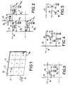
- a LCD display comprises an image forming panel 10 of the transmissive type having a plurality of elementary cells.
- This panel 10 comprises a rear face 12 and a front face 14.
- Illumination means (not represented) provide illumination light 16 on the rear side 12.
- the panel 10 has a general rectangular shape. It is divided in nine areas 10 1 , ..., 10 9 , also with a rectangular shape.
- a photo-detector element 18 1 , ..., 18 9 is provided in each area.
- the photo-detector elements 18 1 , ..., 18 9 control the transmissivity of the image forming elements or picture elements of the corresponding area.
- Figure 2 represents an example of a photo-detector element 18 controlling several elementary cells 20 1 , 20 2 , 20 3 ,
- each elementary cell comprises a liquid crystal (LC) cell 22 i in series with a switching element, such as a transistor 24 i .
- a switching element such as a transistor 24 i .
- One electrode of the LC cell 22 i is connected to ground and its other electrode is connected, through switching element 24 i , to a line 26 receiving a luminance signal L.
- the transistor 24 i has a control electrode 28 i which is connected to a switching line 30 receiving a switching signal S.
- the switching signal S controls the conductivity of transistor 24 i and of other transistors on the same line of panel 10 in such a way that this transistor 24 i is off (non conductive) when the corresponding line is not selected by a scanning device (not represented) and this transistor 24 i is conductive when the corresponding line is selected by the scanning device.
- the intensity of light transmitted by the panel 10 depends on the intensity of the signal L provided by line 26.
- the photo-conductor element 18 provides a further control of the transmissivity of the panel 10. To this end, the photo-detector element controls the conductivity of transistors 24 1 , 24 2 , 24 3 , etc.
- the photo-conductor element 18 is, in this example, a photo-conducive transistor having one terminal connected to a reference voltage (not shown) through a first resistor 32 and another terminal connected to a second control electrode 36 1 , 36 2 , 36 3 , ... of switching transistors 24 1 , 24 2 , 24 3 , ...
- the terminal 35 of transistor 18 which is connected to control electrodes 36 i of the switching transistors 24 i is also connected to ground through a second resistor 34.
- the switching transistors 24 i are two-gate transistors.
- the control provided by photo-transistor 18 is such that the conductivity of transistors 24 i , 24 j decreases when the intensity of the light received by transistor 18 increases. Contrary to classical liquid crystal displays where the switching transistors 24 have only two states - conductive or non-conductive - in the present embodiment the switching transistors operate in an analog way, i.e. their conductivity may vary between zero and maximum conductivity.
- each elementary cell comprises a photo-conductive element.
- the liquid crystal cell 52 1 is in series with switching transistor 54 1 ; the control electrode 58 1 of transistor 54 1 is directly connected to line 30.
- One terminal of transistor 54 1 is connected to the cell 52 1 and the other terminal of this transistor 54 1 is connected to the line 26.
- a static capacity 60 1 is in parallel with the cell 52 1 .
- the transistor 54 1 has photo-resistive properties in such a way that its conductivity decreases when the light it receives increases.
- each switching transistor 64 is controlled individually. However, this switching transistor is controlled by a separate photo-conductive transistor 66. One terminal 68 of this photo-conductive transistor 66 is connected to line 30 through a resistor 70 and its second terminal 72 is connected to ground through another resistor 74. The second terminal 72 of transistor 66 is connected to the control electrode 76 of switching transistor 64.
- the photo-conductive transistor 66 and the resistors 70 and 74 form a transistor inverter circuit. Therefore when the transistor 66 receives a high intensity of light, the voltage on electrode 72 is close to the voltage of the ground and the switching transistor 64 is non-conductive. If the transistor 66 receives a low intensity of light, the voltage of electrode 72 is close to the voltage of line 30 and, in this case, the conductivity of transistor 64 is maximum when line 30 receives a switching signal. Between these two extreme states, the conductivity of transistor 64 depends on the intensity of light received by photo-transistor 66.
- Figure 5 represents a variation of the example represented on figure 4 .
- a photo-transistor 80 is connected between line 30 and ground. If photo-transistor 80 is strongly illuminated, it is fully conductive and, therefore, the switching signal S is shunted to the ground and switching transistor 64' remains non-conductive. If the photo-transistor 80 receives a small quantity of light, it is not conductive and, therefore, switching transistor 64' can be fully controlled by the switching signal S. Between these extreme values of illumination, the conductivity of photo-transistor 80 controls the conductivity of switching transistor 64' and this conductivity depends on the intensity of light received by photo-transistor 80.
- the photo-detecting elements are transistors, other photo-elements may be used such as photo-resistors, photo-diodes, etc.
- each photo-detecting element must be such that it does not reduce significantly the light transmitted by the panel 10. This condition can be easily fulfilled because such elements will be realized with a reduced area.
Landscapes
- Physics & Mathematics (AREA)
- Engineering & Computer Science (AREA)
- Nonlinear Science (AREA)
- General Physics & Mathematics (AREA)
- Chemical & Material Sciences (AREA)
- Crystallography & Structural Chemistry (AREA)
- Mathematical Physics (AREA)
- Microelectronics & Electronic Packaging (AREA)
- Optics & Photonics (AREA)
- Computer Hardware Design (AREA)
- Theoretical Computer Science (AREA)
- Liquid Crystal Display Device Control (AREA)
- Control Of Indicators Other Than Cathode Ray Tubes (AREA)
- Liquid Crystal (AREA)
Claims (4)
- Anzeigevorrichtung, die einen Bilderzeugungsbildschirm (10) umfasst, der mehrere bildbildende Elemente (221) enthält, wobei jedes bildbildende Element mit einem Schaltelement (241), das eine zum Empfangen eines Schaltsignals (s) ausgelegte Steuerelektrode (28i) aufweist, in Reihe geschaltet ist, wobei das Schaltelement dafür ausgelegt ist, in Abhängigkeit von dem Schaltsignal (s) in der Weise ein Helligkeitssignal (L) an das bildbildende Element zu senden, dass die Lichtdurchlässigkeit jedes bildbildenden Elements angesichts des Inhalts des Bildes an dem Ort dieses Elements gesteuert wird, wobei die Anzeigevorrichtung außerdem ein Beleuchtungsmittel auf der Rückseite (12) des Bildschirms und ein Photodetektierungsmittel (18), das dafür ausgelegt ist, die Lichtdurchlässigkeit der bildbildenden Elemente in der Weise zu steuern, dass das angezeigte Bild mit einer gleichförmigen Beleuchtung erscheint, umfasst, wobei das Photodetektierungsmittel mehrere Photodetektorelemente umfasst, dadurch gekennzeichnet, dass jedes Photodetektorelement dafür ausgelegt ist, die Leitfähigkeit der in dem gegebenen Bereich des Bildschirms angeordneten Schaltelemente (241, 242, 243) zu steuern und dadurch die Durchlässigkeit aller in dem gegebenen Bereich angeordneten bildbildenden Elemente zu steuern, wobei jedes Schaltelement in dem gegebenen Bereich eine weitere Steuerelektrode (36i) umfasst, die in der Weise verbunden ist, dass sie ein Signal von dem Photodetektorelement empfängt.
- Anzeigevorrichtung nach Anspruch 1, dadurch gekennzeichnet, dass das Photodetektierungselement eines der folgenden Elemente umfasst: einen Phototransistor, einen Photowiderstand und eine Photodiode.
- Anzeigevorrichtung nach einem der vorhergehenden Ansprüche, wobei die Anzeigevorrichtung eine Flüssigkristallanzeigevorrichtung vom Projektionstyp ist.
- Anzeigevorrichtung nach einem der Ansprüche 1 oder 2, wobei die Anzeigevorrichtung eine Flüssigkristallanzeigevorrichtung vom Direktbetrachtungstyp ist.
Priority Applications (1)
| Application Number | Priority Date | Filing Date | Title |
|---|---|---|---|
| EP97402424.2A EP0909976B1 (de) | 1997-10-14 | 1997-10-14 | Anzeigevorrichtung mit einer bilderzeugenden Tafel und einer Beleuchtungsvorrichtung an deren Rückseite |
Applications Claiming Priority (1)
| Application Number | Priority Date | Filing Date | Title |
|---|---|---|---|
| EP97402424.2A EP0909976B1 (de) | 1997-10-14 | 1997-10-14 | Anzeigevorrichtung mit einer bilderzeugenden Tafel und einer Beleuchtungsvorrichtung an deren Rückseite |
Publications (2)
| Publication Number | Publication Date |
|---|---|
| EP0909976A1 EP0909976A1 (de) | 1999-04-21 |
| EP0909976B1 true EP0909976B1 (de) | 2016-07-27 |
Family
ID=8229878
Family Applications (1)
| Application Number | Title | Priority Date | Filing Date |
|---|---|---|---|
| EP97402424.2A Expired - Lifetime EP0909976B1 (de) | 1997-10-14 | 1997-10-14 | Anzeigevorrichtung mit einer bilderzeugenden Tafel und einer Beleuchtungsvorrichtung an deren Rückseite |
Country Status (1)
| Country | Link |
|---|---|
| EP (1) | EP0909976B1 (de) |
Family Cites Families (2)
| Publication number | Priority date | Publication date | Assignee | Title |
|---|---|---|---|---|
| JPH02251825A (ja) * | 1989-03-24 | 1990-10-09 | Matsushita Electric Ind Co Ltd | 光閾値素子 |
| JPH0611690A (ja) * | 1992-06-26 | 1994-01-21 | Rohm Co Ltd | 液晶表示装置 |
-
1997
- 1997-10-14 EP EP97402424.2A patent/EP0909976B1/de not_active Expired - Lifetime
Also Published As
| Publication number | Publication date |
|---|---|
| EP0909976A1 (de) | 1999-04-21 |
Similar Documents
| Publication | Publication Date | Title |
|---|---|---|
| EP0573045B1 (de) | LCD mit Photosensor | |
| US8624846B2 (en) | Display device | |
| US6851815B2 (en) | Light guide plate with trigonal recesses | |
| EP0601837B1 (de) | Anzeigevorrichtung mit integrierter Bildeingabe | |
| US6700557B1 (en) | Electrode border for spatial light modulating displays | |
| US11156868B2 (en) | Charge release circuit and driving method therefor, and display device | |
| JPS60165621A (ja) | 透過型表示素子 | |
| US3971931A (en) | Led image tube light valve | |
| KR19990014880A (ko) | 디스플레이 장치 | |
| JPS60165624A (ja) | 透過型表示素子 | |
| JP2004518181A (ja) | ディスプレイ | |
| JPH11295691A (ja) | 液晶表示装置と液晶表示パネルの製造方法 | |
| EP0909976B1 (de) | Anzeigevorrichtung mit einer bilderzeugenden Tafel und einer Beleuchtungsvorrichtung an deren Rückseite | |
| US8441471B2 (en) | Light source device and display device including the same | |
| JPS645174A (en) | Projecting television receiver | |
| US5788354A (en) | Projection type display | |
| JPS61285429A (ja) | 液晶フラツトパネルデイスプレイ | |
| JP2958828B2 (ja) | 画像読み取り/表示装置 | |
| EP1384226B1 (de) | REDUZIERUNG DER VORSPANNUNG BEI Räumlichen LICHTMODULATOREN | |
| US6330099B1 (en) | Liquid crystal apron and skirt isolation for silicon micro displays | |
| US8508452B2 (en) | Systems and method for displaying images with reduced power consumption | |
| JP2007304520A (ja) | カラー液晶表示装置 | |
| JPH0361927A (ja) | 液晶表示装置 | |
| WO1991007851A1 (en) | Matrix addressed liquid crystal light valve | |
| KR20060039218A (ko) | 다수의 평판표시패널을 포함하는 평판표시장치 |
Legal Events
| Date | Code | Title | Description |
|---|---|---|---|
| PUAI | Public reference made under article 153(3) epc to a published international application that has entered the european phase |
Free format text: ORIGINAL CODE: 0009012 |
|
| AK | Designated contracting states |
Kind code of ref document: A1 Designated state(s): AT BE CH DE DK ES FI FR GB GR IE IT LI LU MC NL PT SE |
|
| AX | Request for extension of the european patent |
Free format text: AL;LT;LV;RO;SI |
|
| 17P | Request for examination filed |
Effective date: 19990521 |
|
| AKX | Designation fees paid |
Free format text: DE FR GB |
|
| 17Q | First examination report despatched |
Effective date: 20040607 |
|
| REG | Reference to a national code |
Ref country code: DE Ref legal event code: R079 Ref document number: 69740855 Country of ref document: DE Free format text: PREVIOUS MAIN CLASS: G02F0001136000 Ipc: G02F0001136800 |
|
| GRAP | Despatch of communication of intention to grant a patent |
Free format text: ORIGINAL CODE: EPIDOSNIGR1 |
|
| RIC1 | Information provided on ipc code assigned before grant |
Ipc: G02F 1/1368 20060101AFI20131108BHEP Ipc: G09G 3/36 20060101ALI20131108BHEP Ipc: G02F 1/133 20060101ALN20131108BHEP Ipc: G02F 1/135 20060101ALN20131108BHEP |
|
| INTG | Intention to grant announced |
Effective date: 20131219 |
|
| GRAS | Grant fee paid |
Free format text: ORIGINAL CODE: EPIDOSNIGR3 |
|
| GRAA | (expected) grant |
Free format text: ORIGINAL CODE: 0009210 |
|
| AK | Designated contracting states |
Kind code of ref document: B1 Designated state(s): DE FR GB |
|
| REG | Reference to a national code |
Ref country code: GB Ref legal event code: FG4D |
|
| REG | Reference to a national code |
Ref country code: DE Ref legal event code: R096 Ref document number: 69740855 Country of ref document: DE |
|
| REG | Reference to a national code |
Ref country code: DE Ref legal event code: R097 Ref document number: 69740855 Country of ref document: DE |
|
| REG | Reference to a national code |
Ref country code: DE Ref legal event code: R119 Ref document number: 69740855 Country of ref document: DE |
|
| PLBE | No opposition filed within time limit |
Free format text: ORIGINAL CODE: 0009261 |
|
| STAA | Information on the status of an ep patent application or granted ep patent |
Free format text: STATUS: NO OPPOSITION FILED WITHIN TIME LIMIT |
|
| GBPC | Gb: european patent ceased through non-payment of renewal fee |
Effective date: 20161027 |
|
| 26N | No opposition filed |
Effective date: 20170502 |
|
| REG | Reference to a national code |
Ref country code: FR Ref legal event code: ST Effective date: 20170630 |
|
| PG25 | Lapsed in a contracting state [announced via postgrant information from national office to epo] |
Ref country code: DE Free format text: LAPSE BECAUSE OF NON-PAYMENT OF DUE FEES Effective date: 20170503 Ref country code: FR Free format text: LAPSE BECAUSE OF NON-PAYMENT OF DUE FEES Effective date: 20161102 Ref country code: GB Free format text: LAPSE BECAUSE OF NON-PAYMENT OF DUE FEES Effective date: 20161027 |