Background of the Invention
Head mounted display systems have been developed
for a number of different applications including use by
aircraft pilots and for simulation. Head mounted
displays are generally limited by their resolution and
by their size and weight. Existing displays have
relatively low resolution and are positioned at a
relatively large distance from the eye. Of particular
importance, is to keep the center of gravity of the
display from extending upward and forward from the
center of gravity of the head and neck of the wearer,
where it will place a large torque on the wearer's neck
and may bump into other instruments during use. There
is a continuing need to present images to the wearer of
a helmet mounted display in a high-resolution format
similar to that of a computer monitor. The display
needs to be as non-intrusive as possible, leading to
the need for a lightweight and compact system.
Head mounted displays can also utilize eye
tracking systems in flight control, flight simulation
and virtual imaging displays. Eye control systems
generate information based on the position of the eye
with respect to an image on a display. This
information is useful for a variety of applications.
It can be used to enable the viewer to control "hands-free"
movement of a cursor, such as a cross-hair on the
display.
Apparatus for detecting the orientation of the eye
or determining its line-of-sight (LOS) are called
occulometers or eye trackers and are well known in the
art. (See for example U.S. 4,109,145, 4,034,401 and
4,028,725).
Summary of the Invention
In accordance with the present invention a head
mounted display is preferably either an
electroluminescent (EL,) or an active matrix liquid
crystal display (AMLCD) comprising thin film transistor
(TFT) driving elements formed of single crystal silicon
and then transferred to a transparent glass substrate.
Each TFT circuit is connected to an electrode which
defines a picture element (pixel) of the display. The
head mounted display system can also include a detector
array comprising thin film integrated optical diode
detectors is formed of III-V materials and transferred
directly onto a flat panel active matrix display.
In a preferred embodiment of a direct view eye
tracking display, the detectors are positioned such
that each is completely above the drive transistors of
the active matrix circuit i.e., adjacent to the pixel
area and therefore do not block any of the display's
light output. The light output from the display,
either infrared or visible, is used to determine the
position of the eye. No additional optics, such as,
fiber optics to/from remote displays are required in
this approach. The chief advantage is that the
integrated eyetracker/display can be inserted in a
helmet-mounted optical system without physical
modification to the helmet or optics. This advantage
results from the fundamental reciprocity of the axial
light rays that are used to determine the eye position.
An axial ray, is a light ray that emanates from the
display and travels through the optical axis of the
eye, normal to the retina. These rays, when reflected
by the retina, can travel back to the display along the
same optical path (in accordance with the optical
reciprocity theorem). Except for divergence of the
rays, the reflected rays return to the vicinity of the
emitting pixel. In this way, the detector can identify
the area of the display that is sighted by the user.
Software in a computer then provides a cursor at this
location.
In another alternative embodiment, instead of
using the visible scene from the display, some of the
frames in the display are used for brief presentation
of an interlaced eyetracker pattern. If the repetition
rate of the test pattern is sufficiently infrequent,
the user (viewer) will not perceive its presence. This
pattern can consist of a single pixel being illuminated
or can have some other geometric pattern. Light from a
single lit pixel enters the eye through the pupil and
is reflected from the retina. The path of the
reflected light clearly depends on the position of the
eye. On the reverse path back to the display panel,
the reflected light undergoes spreading or convergence
depending upon the optical system. As it returns to
the plane of the display, it strikes the
photodetectors. A pattern will appear in the output of
the photodetector array that depends on the position of
the eye and the nature of the optical system. This
pattern is interpreted by a computer and correlated to
the position of the eye.
The present invention uses a single-crystal
material to produce a high-density active matrix array
in a head mounted optical support system that provides
for closeness of the display to the eye, compactness of
the array and provides the desired level of resolution.
With a density of 400 lines per centimeter, for
example, a 1.27 centimeters display in accordance with
the invention will fit into a system only 1.52
centimeters in depth. This system is more compact, has
lighter weight, and a lower cost than existing head
mounted displays.
To get the display system as close as possible to
the eye and as compact as possible, a short focal
length lens system must be used. The focal lengths of
simple lenses are limited by lens geometry, where the
thickness of the lens is less than the lens diameter.
Thus, a simple lens has a shorter focal length as well
as a small diameter. For the most compact system, the
smallest possible lens that focuses the display image
is used. The lens size is defined by the object size,
which in this case is the size of the display element.
Since resolution needs to be increased while size
needs to be decreased, the pixel density of the display
needs to increase. Existing displays have pixel
densities of about 120 lines per centimeter and are
about 4.1 centimeters in diameter. Using a 3.81
centimeter lens, where the minimum focal length for a
standard 3.81 centimeter lens is about 3.05
centimeters, results in a lens with a center thickness
of over 1.52 centimeters. The use of this lens results
in a lens-to-display distance of about 3.3 centimeters,
which is the minimum depth of an existing head-mounted
display for this geometry.
The present system, by increasing the pixel
density to at least 200 lines per centimeter, and
preferably to over 400 lines per centimeter, provides
for a lens-to-display distance of less than one inch.
The lens-to-display distance is preferably in the range
of 1.0-2.2 centimeters.
The display can be a transmission type-display
with the light source directly adjacent the light valve
active matrix or the light source can be positioned
above the head or to one or both sides of the head of
the user such that the light can be coupled to the
light valve active matrix by one or more reflective
elements. Fiber optics can also be employed to provide
a back light source for the display or to deliver
images from the display into the user's field of view.
Alternatively, the display can be an emission type
device such as an active matrix electroluminescent
display or an active matrix of light emitting diodes
(LEDs).
Additional embodiments of the invention include a
projected view active matrix display in which different
polarization components of light are separated, one
component being directed to the left eye, and another
component being directed to the right eye. This
provides a more efficient optical system in which more
light from the source is used to provide the desired
image.
Another preferred embodiment utilizes an active
matrix display in which the pixel size increases across
the display to provide a wide angle field of view
display.
The display can be fabricated as a visor with a
number of displays which are tiled together and
positioned on a flat or curved plastic visor.
Brief Description of the Drawings
Figure 1 is a perspective view of a high density
circuit module in the form of an active matrix liquid
crystal display (AMLCD).
Figure 2A is a schematic illustrating how two six
inch wafers can be used to form tiles for a 4 X 8 inch
AMLCD.
Figure 2B shows the tiles of Figure 2A applied to
a glass substrate for forming an AMLCD.
Figure 3 is a circuit diagram illustrating the
driver system for the AMLCD of Figure 1.
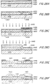
Figures 4A-4L is a preferred process flow sequence
illustrating the fabrication of the a portion of the
circuit panel for the AMLCD of Figure 1.
Figures 5A and 5B are cross-sectional schematic
process views of a portion of the AMLCD.
Figure 6 illustrates in a perspective view a
preferred embodiment of a system used for
recrystallization.
Figures 7A-7D is a process flow sequence
illustrating transfer and bonding of a silicon an oxide
(SOI) structure to a glass superstrate and removal of
the substrate.
Figures 8A and 8B is a process flow sequence
illustrating an alternative transfer process in which a
GeSi alloy is used as an intermediate etch step layer.
Figure 9 is a schematic diagram of an eye tracking
system of the invention.
Figure 10 is a schematic of an alternate
embodiment of an eye tracking system of the invention.
Figure 11 is an exploded view of the integrated
display/detector array panel (eye-tracker) of the
invention.
Figure 12 is a plan view of a simplified version
of the eye tracker in which the matrix array
metallization is replaced by a common parallel
interconnect.
Figures 13A-13C are cross-sectioned views showing
important steps in the process of forming the eye-tracker
device of the invention.
Figures 14A-B are schematic section views of a
wafer being processing to form an X-Y addressable LED
array.
Figures 14C-E are schematic partial perspectives
showing a wafer during successive additional process
steps.
Figures 15A-15B is a process flow diagram of the
main steps in fabricating an LED bar in accordance with
a mesa etch isolation process with a corresponding
schematic sectional view of a wafer structure so
processed shown beneath each step.
Figure 16 is a cross-sectional side view of a
wafer during step k of Figure 15b.
Figure 17 is a process flow diagram of the main
steps in fabricating an LED bar in accordance with an
alternate process with a correspnding schematic
sectional view of a wafer structure so processed shown
beneath each step.
Figures 18A-18B is a process flow diagram of the
main steps in fabricating an LED bar in accordance with
yet another alternate process with a corresponding
schematic sectional view of a wafer structure so
processed shown beneath each step.
Figure 19 is a plan view of an X-Y addressable LED
array mounted on a silicon substrate with associated
silicon electronic circuitry.
Figure 20 is a perspective view of a LED pixel
from an X-Y addressable LED array embodiment of the
invention.
Figure 21 is a schematic side view of an IR to
visible light converter embodiment of the invention.
Figure 22 is a schematic diagram of the converter
of Figure 21.
Figure 23 is a side view of an alternate
embodiment of Figure 21.
Figure 24 is a side view of a pixel of a tri-color
X-Y addressable LED array.
Figure 25 is a plan view of the array of Figure
24.
Figure 26 is a schematic diagram of an alternate
embodiment of an eye tracking device of the invention.
Figure 27A is an exploded perspective view of an
electroluminescent panel display in accordance with the
present invention.
Figure 27B is a perspective view of an
electroluminescent color display element.
Figure 27C is a circuit diagram illustrating the
driver system for the electroluminescent panel display.
Figure 27D is an equivalent circuit for a DMOS
transistor of Figure 16C.
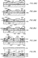
Figures 28A-28L is a preferred process flow
sequency illustrating the fabrication of a circuit
panel for an electroluminescent panel display.
Figures 29A-29D is preferred process flow sequence
illustrating the fabrication of an electroluminescent
color display.
Figures 30A-30B is a preferred process flow
sequence illustrating transfer and bonding of an SOI
structure to a superstrate and removal of the
substrate.
Figures 31A-31B is a preferred process flow
sequence illustrating an alternative transfer process
in which a GeSi alloy is used as an intermediate etch
stop layer.
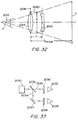
Figure 32 shows a schematic illustration of a head
mounted display system.
Figure 33 illustrates a preferred embodiment of a
head mounted display where two components of polarized
light are separated for improved optical efficiency.
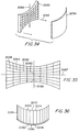
Figure 34 illustrates an active matrix for a wide
angle field of view head mounted display system.
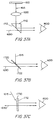
Figure 35 provides a detailed view of a portion of
the active matrix area of the device shown in Figure
34.
Figure 36 illustrates an active matrix mounted or
tiled onto a visor screen.
Figure 37A-37C illustrates other preferred
embodiments of a direct-view display system.
Detailed Description of the Invention
I. Tiled Active Matrix Liquid Crystal Display
A preferred embodiment of the invention for
fabricating complex hybrid multi-function circuitry on
common module substrates is illustrated in the context
of an AMLCD for a head mounted display, as shown in
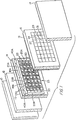
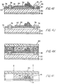
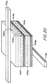
Figure 1. The basic components of the AMLCD comprise a
light source 10, such as a flat fluorescent or
incandescent white lamp, or an electroluminescent lamp
having white, or red, blue and green phosphors, a first
polarizing filter 12, a circuit panel 14, an optional
filter plate 16 and a second polarizing filter 17,
which form a layered structure. Note that filter plate
16 is not needed for a black and white display or where
the red, green and blue colors are provided by the lamp
at the appropriate pixel. A liquid crystal material
19, such as a twisted nematic is placed between the
circuit panel 14 and the filter plate 16.
Circuit panel 14 consists of a transparent common
module body 13 formed, for example, of glass upon which
is transferred a plurality of common multifunction
circuits comprising control logic circuits 40A and 40B
and drive circuits 18A and 18B, 20A and 20B, and array
circuit 25A and 25B. Preferably, the logic and drive
circuits which require high speed operation are formed
in tiles of x-Si. The array circuits may be formed in
α-Si material, or poly-Si, or preferably in x-Si, to
achieve lower leakage in the resultant TFT's and,
hence, better grey scale. Higher speed is also
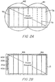
achieved in x-Si. Displays as large as a 4 x 8 inch
active matrix LCD array can be formed from two standard
6-inch diameter Si wafers W1 and W2 as shown in Figure
2A. Array circuit 25A is formed on wafer W1 and 1-inch
by 4-inch tiles TA are transferred from the wafer W1 to
the substrate 14. Note that the transfer can be
accomplished using either a single or double transfer
process, as will be described in detail below. Each
tile is registered against another using
micropositioning equipment and manipulators capable of
micron scale accuracy. Similarly, tiles TB are
transferred from wafer W2 to form array 25B on
substrate or common module body 13 (See Figure 2B).
Logic circuits 40A and 40B and drive circuits 18A,
18B, 20A, 20B are formed on other suitable substrates
(not shown) and tiled and transferred in like manner to
common substrate 13 and registered opposite the arrays
25A, 25B, as shown in Figure 1. Conductive
interconnections 50 are then made between the drive
circuits and the individual pixels 22 and the logic
control circuits 40A and 40B. In this manner, a 1280
by 1024 addressable array of pixels 22 are formed on
the substrate 13 of circuit panel 14. Each pixel 22 is
actuated by voltage from a respective drive circuit 18A
or B on the X-axis and 20A or B on the Y-axis. The X
and Y drive circuits are controlled by signals from
control logic circuits 40A and B. Each pixel 22
produces an electric field in the liquid crystal
material 19 disposed between the pixel and a
counterelectrode (not shown) formed on the back side of
the color filter plate 16.
The electric field formed by pixels 22 causes a
rotation of the polarization of light being transmitted
across the liquid crystal material that results in an
adjacent color filter element being illuminated. The
color filters of filter plate system 16 are arranged
into groups of four filter elements, such as blue 24,
green 31, red 27, and white 29. The pixels associated
with filter elements can be selectively actuated to
provide any desired color for that pixel group.
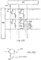
A typical drive and logic circuit that can be used
to control the array pixels 22 is illustrated in Figure
3. Drive circuit 18A receives an incoming signal from
control logic 40A and sends a signal to each source
electrode of a TFT 51 in one of the columns selected by
logic circuit 40A through interconnect line 53. Y-drive
circuit 20A controlled by logic circuit 40A
energizes a row buss 59 extending perpendicular to
column buss 53 and applies a voltage pulse to each gate
G of TFT's 51 in a selected row. When a TFT has a
voltage pulse on both its gate and source electrode
current flows through an individual transistor 51,
which charges capacitor 56 in a respective pixel 22.
The capacitor 56 sustains a charge on the pixel
electrode adjacent to the liquid crystal material
(shown schematically at 19) until the next scan of the
pixel array 25. Note that the various embodiments of
the invention may, or may not, utilize capacitors 56
with each pixel depending upon the type of display
desired.
II. Transfer Processes
The array circuits 25A and 25B and logic 40A, 40B
and drive circuits 18A,18B may be formed and
transferred by a number of processes. The basic steps
in a single transfer process are: forming of a
plurality of thin film Si circuits on Si substrates,
dicing the thin film to form tiles, and transferring
the tiles to a common module substrate by "tiling."
Tiling can also be employed in fabricating III-V
material circuits or hybrid Si and III-V material
circuits or circuit components, which can be stacked to
provide compact modules.
Tiling involves the steps of transferring,
registering the transferred tiles, and adhering the
registered tiles. The Si substrates are then removed
and the circuits on the tiles are interconnected. The
double transfer approach, described in detail below in
connection with Figures 4A-4L is similar except that
the Si-substrate is removed after dicing and the thin
film is transferred to an intermediate transfer body or
carrier before ultimate transfer to the common module
body.
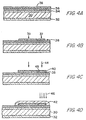
Assuming an Isolated Silicon Epitaxy (ISE) process
is used, the first step is to form a thin-film
precursor structure of silicon-on-insulator (SOI) film.
An SOI structure, such as that shown in Figure 4A,
includes a substrate 32 of Si, a buffer layer 30, of
semi-insulating Si and an oxide 34 (such as, for
example, SiO2) that is grown or deposited on buffer
layer 30, usually by Chemical Vapor Deposition (CVD).
An optional release layer 36 of material which etches
slower than the underlying oxide layer 34 is then
formed over the oxide 34.
For example, a silicon oxy-nitride release layer,
comprising a mixture of silicon nitride (S3N4) and
silicon dioxide (SiO2) may be a suitable choice. Such
a layer etches more slowly in hydrofluoric acid than
does SiO2 alone. This etch rate can be controlled by
adjusting the ratio of N and O in the silicon oxynitride
(SiOxNy) compound.
A thin essentially single crystal layer 38 of
silicon is then formed over the release layer 36. The
oxide (or insulator) 34 is thus buried beneath the Si
surface layer. For the case of ISE SOI structures, the
top layer is essentially single-crystal recrystallized
silicon, from which CMOS circuits can be fabricated.
Note that for the purposes of the present
application, the term "essentially" single crystal
means a film in which a majority of crystals show a
common crystalline orientation and extend over a cross-sectional
area in a plane of the film for at least 0.1
cm2, and preferably, in the range of 0.5 - 1.0 cm2, or
more. The term also includes completely single crystal
Si. The thin films can have thicknesses in the range
of 0.1 - 20 microns and preferably in the range 0.1 -
1.0 microns.
The use of a buried insulator provides devices
having higher speeds than can be obtained in
conventional bulk (Czochralski) material. Circuits
containing in excess of 1.5 million CMOS transistors
have been successfully fabricated in ISE material. An
optional capping layer (not shown) also of silicon
nitride may also be formed over layer 36 and removed
when active devices are formed. As shown in Figure 4B,
the film 38 is patterned to define active circuits,
such as a TFT's in region 37 and a pixel electrode
region at 39 for each display pixel. Note that for
simplification, only one TFT 51 and one pixel electrode
62 is illustrated (Figure 4H). It should be understood
that an array of 1280 by 1024 such elements can in
practice be formed on a single 6-inch wafer.
A plurality of arrays may be formed on a single
six-inch wafer, which can then applied to the display
as tiles and interconnected. Alternatively, the
plurality of pixel matrices from one wafer can be
separated and used in different displays. The
plurality may comprise one large rectangular array
surrounded by several smaller arrays (to be used in
smaller displays). By mixing rectangular arrays of
different areas, such an arrangement makes better use
of the total available area on a round wafer.
An oxide layer 40 is then formed over the
patterned regions including an insulator region 48
formed between the two regions 37, 39 of each pixel.
The intrinsic crystallized material 38 is then
implanted 44 (at Figure 4C) with boron or other p-type
dopants to provide a n-channel device (or
alternatively, an n-type dopant for a p-channel
device).
A polycrystalline silicon layer 42 is then
deposited over the pixel and the layer 42 is then
implanted 46, through a mask as seen in Figure 4D, with
an n-type dopant to lower the resistivity of the layer
42 to he used as the gate of the TFT. Next, the
polysilicon 42 is patterned to form a gate 50, as seen
in Figure 4E, which is followed by a large implant 52
of boron to provide p+ source and drain regions 66, 64
for the TFT on either side of the gate electrode. As
shown in Figure 4F, an oxide 54 is formed over the
transistor and openings 60, 56, 58 are formed through
the oxide 54 to contact the source 66, the drain 64,
and the gate 50. A patterned metallization 71 of
aluminum, tungsten or other suitable metal is used to
connect the exposed pixel electrode 62 to the source 66
(or drain), and to connect the gate and drain to other
circuit panel components.
The devices have now been processed and the
circuits may now be tested and repaired, as required,
before further processing occurs.
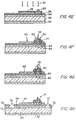
The next step in the process is to transfer the
silicon pixel circuit film to a common module, either
directly, or by a double transfer from substrate to
carrier and then to the common module. A double
transfer approach is illustrated in Figures 4H-4L. To
separate a circuit tile from the buffer 30 and
substrate 37, a first opening 70 (in Figure 4H) is
etched in an exposed region of release layer 36 that
occurs between tiles. Oxide layer 34 etches more
rapidly in HF than nitride layer 36, thus a larger
portion of layer 34 is removed to form cavity 72. A
portion of layer 36 thus extends over the cavity 72.
In Figure 4I, a support post 76 of oxide is formed
to fill cavity 72 and opening 70, which extends over a
portion of layer 36. Openings or via holes 74 are then
provided through layer 36 such that an etchant can be
introduced through holes 74, or through openings 78
etched beneath the release layer 36, to remove layer 34
(See Figure 4J). The remaining release layer 36 and
the circuitry supported thereon is now held in place
relative to substrate 32 and buffer 30 with support
posts 76.
Next, an epoxy 84 that can be cured with
ultraviolet light is used to attach an optically
transmissive superstrate 80 to the circuitry, and layer
36. The buffer 30 and substrate 32 is then patterned
and selectively exposed to light such that regions of
epoxy 84' about the posts 76 remain uncured while the
remaining epoxy 84' is cured (See Figure 4K). The
buffer 30 and substrate 32 and posts 76 are removed by
cleavage of the oxide post and dissolution of the
uncured 84 epoxy to provide the thin film tile
structure 141, shown in Figure 4L mounted on carrier
80.
To form the final display panel, the edges of the
carrier 80 are trimmed to coincide with the tile
borders. The nitride release layer 36 is removed by
etching.
As shown in Figure 5A, a plurality of tile
structures 141 are then sequentially registered with
one another and adhered to a common module body 110
using a suitable adhesive (not shown). Common module
body 110 is preferably patterned with interconnect
metallization on the surface facing the tile structure
141 for interconnecting individual tile circuitry with
each other. Next, insulation and alignment layers,
spacers, a sealing border and bonding pads for
connections (not shown) are bonded onto the periphery
of the common module body 110. A screen printing
process can be used to prepare the border. As shown in
Figure 5B, a plate 117 containing the color filters 120
and the counterelectrode (not shown) is bonded to the
periphery thin film circuit tiles 141 with the sealing
border after insertion of spacers (not shown). The
display is filled with the selected liquid crystal
material 116 via a small filling hole or holes
extending through the border. This filling hole is
then sealed with a resin or epoxy. First and second
polarizer films 118, 112 or layers are then bonded to
both sides and connectors (not shown) are added.
Finally, a white light source 114, or other suitable
light source, is bonded to polarizer 112.
Pixel electrodes 62 are laterally spaced from each
other. Each pixel has a transistor 51 and a color
filter 120 or 122 associated therewith. A bonding
element or adhesive 82 and optically transmissive
superstrate 110, such as glass or plastic completes the
structure. Body 110 is preferably a low temperature
glass that can have a thickness preferably of about 200
to 1000 microns.
In an alternative CLEFT process, thin single-crystal
films, are grown by chemical vapor deposition
(CVD), and separated from a reusable homoepitaxial
substrate.
The films removed from the substrate by CLEFT are
"essentially" single-crystal, of low defect density,
are only a few microns thick, and consequently, circuit
panels formed by this process have little weight and
good light transmission characteristics.
The CLEFT process, illustrated in U.S. Patent No.
4,727,047, involves the following steps: growth of the
desired thin film over a release layer (a plane of
weakness), formation of metallization and other
coatings, formation of a bond between the film and a
second substrate, such as glass (or superstrate), and
separation along the built-in-plane of weakness by
cleaving. The substrate is then available for reuse.
The CLEFT process is used to form sheets of
essentially single crystal material using lateral
epitaxial growth to form a continuous film on top of a
release layer. For silicon, the lateral epitaxy is
accomplished either by selective CVD or, preferably, a
lateral recrystallization or ISE process, or other
recrystallization procedures. Alternatively, other
standard deposition techniques can be used to form the
necessary thin film of essentially single crystal
material.
One of the necessary properties of the material
that forms the release layer is the lack of adhesion
between the layer and the semiconductor film. When a
weak plane has been created by the release layer, the
film can be cleaved from the substrate without any
degradation. As noted in connection with Figures 4A-4C,
the release layers can comprise multi-layer films
of Si3N4 and SiO2. Such an approach permits the SiO2 to
be used to passivate the back of the CMOS logic. (The
Si3N4 is the layer that is dissolved to produce the
plane of weakness.) In the CLEFT approach, the
circuits are first bonded to the glass, or other
transfer substrate, and then separated, resulting in
simpler handling as compared to, for example, UV-cured
tape.
The plane of weakness is key to obtaining uniform
cleaving between the circuits and the substrate. This
plane may be formed by creating a pattern of carbon on
the surface of the wafer so that only a small fraction
of the underlying semiconductor surface is exposed.
These exposed portions are used as nucleation cites for
the epitaxial film. If the growth conditions are
properly chosen, the film will grow laterally faster
than vertically, leading to laterial overgrowth of the
single crystal film. Within 1µm of vertical growth,
the film becomes continuous and of high quality.
However, the carbon layer is weak and, combined with
the small fraction of exposed semiconductor areas where
the film is strongly attached to the substrate, creates
a plane of weakness. This plane can be used reliably
and reproducibly to separate the film from the
substrate. The substrate may be reused. These
processes have been used to transfer a wide range of
GaAs and Si circuits to alternative substrates such as
glass, ceramic, and other materials, without harm to
the active circuitry.
In the ISE process, the oxide film is strongly
attached to the substrate and to the top Si film which
will contain the circuits. For this reason, it is
necessary to reduce the strength of the bond
chemically. This requires use of a release layer that
is preferentially dissolved with an etchant without
complete separation to form a plane of weakness in the
release layer. The films can then be separated
mechanically after the glass is bonded to the circuits
and electrodes.
Mechanical separation may be accomplished by
bonding the upper surface of the Si film to a
superstrate, such as glass, using a transparent epoxy.
The film and glass are then bonded with wax to glass
plates about 5 mm thick that serve as cleaving
supports. A metal wedge is inserted between the two
glass plates to force the surfaces apart. Since the
mask has low adhesion to the substrate, the film is
cleaved from the substrate but remains mounted on the
glass. The substrate can then be used for another
cycle of the CLEFT process, and the device processing
may then be completed on the back surface of the film.
Note that since the device remains attached to a
superstrate, the back side can be subjected to standard
wafer processing, including photolithography.
One embodiment of the invention utilizes a
recrystallization system, shown schematically in Figure
6 to form the essentially single crystal Si thin film.
A sample wafer 134 is formed of poly Si, formed on
SiO2, formed on an Si wafer. A capping layer 138 is
formed over the poly Si. The wafer temperature is then
elevated to near the melting point by a lower heater
130. An upper wire or graphite strip heater 132' is
then scanned across the top of the sample 134 to cause
a moving melt zone 136 to recrystallize or further
crystallize the polycrystalline silicon. The lateral
epitaxy is seeded from small openings formed through
the lower oxide. The resultant single crystal film has
the orientation of the substrate.
A number of unique devices and circuits have been
formed using the above processing techniques. These
techniques have been used to transfer CMOS active
matrix LCD circuitry from ISE wafers to glass, and have
yielded excellent displays with single crystal Si
active matrix circuits. Silicon circuitry has been
transferred to glass and shows no important changes in
transistor characteristics after transfer. The
technique has also been proved with III-V compound
semiconductor circuits. For example, GaAs and AlGaAs
monolithic series-connected photovoltaic energy
converters have been made for power down a fiber
application that yield exceptional performance. Also,
two-dimensional multiplexed AlGaAs LED arrays (with
over 32K pixels) have been made by transfer and two-sided
processing and exhibit extremely high LED density
as well as performance. The development of this broad
range of Si and III-V circuits indicates the general
applicability of the transfer process to a wide range
of devices and circuits.
III. Alternate Adhesion and Transfer Processes
Figures 7A-7D illustrate an alternate preferred
double transfer process for adhering and transferring
tiles of circuits of thin films of silicon to a common
module body. The starting structure is a silicon wafer
118 upon which an oxide layer 116 and a thin film of
poly-Si, α-Si or x-Si 114 is formed using any of the
previously described processes such as ISE or CLEFT. A
plurality of circuits, such as pixel electrodes, TFT's,
Si drivers and Si logic circuits, are then formed in
the thin film. Figure 7A shows three such wafers, I,
II, III. In wafer I, logic circuits 40 are formed. In
wafer II, pixel electrodes 62 and TFT's 51 are formed.
In wafer III, driver circuits 20 are formed. A wafer,
or individual tiles diced from the wafer, is attached
to a superstrate transfer body 112, such as glass or
other transparent insulator, using an adhesive 120'.
The adhesive can comprise commercially available
epoxies.
The wafer, or tile, is then cleaned and the native
oxide 118 is etched off the back surface. Depending on
the thickness of the wafer, it may take up to 5 hours
to etch the Si 118 and oxide 116' layers. The solution
etches silicon very rapidly, i.e. 2 to 3 microns/min.,
and uniformly if the wafers are held horizontally in
the solution with the etching surface face up. The
acid has a very low etch rate on oxide, so that as the
substrate is etched away and the buried oxide is
exposed, the etching rate goes down. The observer can
monitor the process and to stop the etch in the buried
oxide layer 116' without punching through to the thin
silicon layer 114 above it. Wafers up to 25 mils thick
and oxides as thin as 4000Å have been successfully
etched using this process. An alternative etchant is
hydrazine, which has a much higher etch rate
selectivity or ethylene diamine pyrocatacol (EDP).
When the silicon is completely gone, the vigorous
bubbling, which is characteristic of silicon etching
abruptly stops, signalling that the etching is
complete.
The thin films 114 transferred to the respective
glass superstrates 112 are now rinsed and dried. If
not already provided with circuits 40, 51, 62 or 20,
the films 114 can be backside circuit processed, if
desired.
After all the necessary circuits are formed, as
above, on transfer bodies 112, they may now be diced
and tiled onto a common module body 13 (Figure 7D) to
perform a combined function, such as an AMLCD. The
system can then be mounted on a helmet or head-mountable
frame for direct or indirect viewing by the
user.
The logic circuits 40 of transfer body 118 in col.
A, Figure 7C, are transferred to the border of module
body 13, while the driver circuits 20 from the transfer
body 118 in col. C, Figure 7C, are disposed on the
border between the logic circuits 40A and 40B.
Tiles of pixel electrodes 62 and TFT's 51 are
formed by dicing or etching and are registered with
respect to each other and pre-formed wiring 50 on
module body 13, as shown in Figure 7D.
After all the circuits are registered and adhered
to the module body, the transfer body 118 and the epoxy
120 is removed using a suitable etchant, such as HF for
the case of a glass transfer body.
Interconnection of circuits is achieved during
registration or by direct laser writing where
necessary. Also, if desired, the film can be
transferred to another substrate and the first glass
superstrate and adhesive can be etched off, allowing
access to the front side of the wafer for further
circuit processing.
Figures 8A and 8B illustrate an alternative one-step
silicon thin film transfer process in which GeSi
is used as an intermediate etch stop layer. In this
process, Si buffer layer 126 is formed on an x-Si
substrate 128 followed by a thin GeSi layer 129 and a
thin α-Si, poly-Si, or x-Si device or circuit layer
132; using well-known CVD or MBE growth systems.
The layer 132 is then IC processed in the manner
previously described in connection with Figures 4E-H,
to form circuits, such as TFT's 200 and pixel
electrodes 202 (Figure 8A). Next, the processed
wafers, or tiles from the wafer, are mounted on a
common module glass (or other) support 280 using an
epoxy adhesive of the type previously mentioned in
connection with Figures 7A-7B. The epoxy fills in the
voids formed by the previous processing and adheres the
front face to the superstrate 280.
Next, the original Si substrate 128 and Si buffer
126 are removed by etching, which does not affect the
GeSi layer 129 (Figures 8B). Finally, the GeSi layer
124 is removed by brief submersion in a suitable etch.
IV. Eve Tracker Embodiment
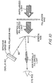
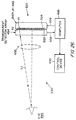
Referring now to the schematic diagram of Figure
9, it may be seen that the present invention relates to
an eye tracking system 410 that combines a flat panel
display device 412 with an array of optical detectors
14 to form an eye tracker device 500. The flat panel
display device is used as a monolithic substrate and
light source for determining the position of the eye
432. The detector array 414 is aligned and transferred
onto the active matrix electronics of the flat panel
device. A test pattern and software in computer 418
analyzes the sensed data generated by the detector on
display and determines the position of the eye.
Light from display 412 is used to project an image
onto viewing screen 428 for viewing by the eye(s) 432
of a viewer. The image to be displayed is generated in
computer 418 and is coupled as an electrical input
video signal to display 412 along line 424. Image
light rays from display 412 pass through detector array
14 and are projected onto screen 428 where they may be
superimposed on external images from an outside scene
formed by light rays C.
A video signal source provides video signals to
the display device 412. The video signal source can be
any analog or digital video signal source including a
Video Graphics Array (VGA) adaptor, National Television
Systems Committee (NTSC) composite video source, high-resolution
professional display adapters, Charge-Coupled-Devices
(CCD), or other similar sources. In a
preferred embodiment a CCD camera is mounted on the
head mounted system so as to generate an image of the
surroundings of the user and which is linked to the
display of the head mounted system. This permits the
user to look in a particular direction and receive an
image on his/her display or viewing screen from the
surrounding area. The display can be programmed to
overlay selected images onto the sensed image. The eye
tracker can be used to enhance the resolution of the
image region that the user's eyes are directed upon.
Horizontal and vertical synchronization signals from
the video signal source are provided to a video
interface. Red-Green-Blue (RGB) video signal
components, if supplied by the video signal source, are
provided to an encoder. If discrete red, green and
blue signals are not supplied by the video source
(e.g., NTSC composite video signal), then a single
video signal must be supplied by the video source.
The display device 412 operates as a multi-frequency
display device. Typically, video signals
from the video signal source will not be synchronized
to a fixed frequency. For example, a VGA adaptor
generates synchronization signals that vary depending
on the particular video mode in which the adaptor is
operating. A standard VGA adaptor may generate a
vertical synchronization frequency between about 56 and
70 Hz and a horizontal synchronization frequency
between about 15 and 35 kHz. For professional display
purposes (e.g., CAD/CAM) the vertical and horizontal
synchronization frequency may be higher than described.
To handle current high resolution displays, the display
device 412 must adapt to vertical synchronization
frequencies up to about 100 Hz and horizontal
synchronization frequencies up to about 66 kHz.
Consequently, the display device 412 adapts to changes
in the synchronization frequencies.
A light ray emanating from a particular pixel of
display 412 is shown as line B2. This ray is reflected
by the screen 428 (line B1) onto the eye optics (not
shown) and on to the macula (not shown) of eye 432.
The axial rays of greatest importance will impinge on
the fovea of the eye, the most sensitive part of the
macula. These rays return to the display in the
vicinity of the original pixel because reflection from
the fovea is approximately normal to the retina and
therefore nearly axial. Non-axial rays which will
impinge on the retina beyond the fovea will not be
reflected back along the axial optical path and will
not return to the detector array 414.
The viewing screen 428 can comprise, for example,
the visor of a heads-up helmet mounted optical system
for pilots and the integrated detector/display can be
inserted in a helmet-mounted optical system without
physical modification to the helmet or optics.
Additionally, no physical contact with the eye is
required.
Once the axial rays B1, B2 return to the display,
the detector array 14 identifies the portion of the
array from which the axial ray emanated, by generating
a voltage signal by a detector pixel located in the
array nearest the returned ray. That portion of the
array is, of course, the part of the display focussed
on by the user. A test pattern from computer 418 is
then interlaced with the display image to enable
initial determination of the eye's position. Software,
in computer 418, provides a cursor image for display
412 which is projected on screen 428 at the line-of-sight
location. This cursor is interlaced to provide
constant feedback to the detector array 414. The
interlace frequency can be adjusted to make the cursor
visible or not visible to the user.
For the case of a partially transparent system of
Figure 9 in which scenes from the surroundings are
superimposed on the display image, the detector array
414 is provided with a narrow band pass filter overlay
to reject all wavelengths except the wavelength of the
cross hair or cursor, which must be one of the display
primary colors. Suppose for example that the selected
color is primary red. In this case, a narrow band red
rejection filter 430 is placed on the outside of the
screen 428, and a narrow red bandpass filter 416 is
placed over the pixels of the detector array 414. In
this way, the detector array 414 only receives light
originating from the display. A second method of
accomplishing the same result is to use polarizing
filters as shown in Figure 10. In this case the flat
panel display 412 is an AMLCD light valve helmet or
head mounted display (HMD), having a polarizer 440 on
its output face. The polarized nature of the light
from the display 440, combined with a 90° crossed
polarizer 442 on the screen 428, prevents unwanted
light from the outside scene from propagating to the
detector array. Further partially transparent imaging
systems are described below in connection with Figures
37A-37C.
Another alternative is to chop or rapidly blink
the video signals from computer 418 for the cursor
presentation so that software in the computer can
subtract the background light. Yet, another
alternative that can be used with LCD displays is to
use infrared light that can pass through the red
filters of the LCD. But this approach requires an IR
rejection filter on the front of the viewing screen.
It can be seen from the above that there are a number
of methods of using the display 412 to provide a signal
for the detector array 414, without interference from
outside light.
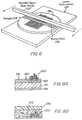
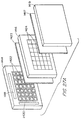
An exploded view of an AMLCD display and
monolithic detector array 414 in accordance with the
invention is illustrated in Figure 11. Note that a
complete eye-tracker package can be made without
substantially changing the overall dimensions of the
display. As shown in Figure 11, a detector array 414
is formed of a III - V diode array 450 transferred to a
glass substrate 452 or directly above and onto front
glass 454 of an active matrix LCD display 412. The
detector pixels 462 are positioned so that each is
completely above the drive transistors 464 of the
active matrix circuit and therefore do not block any of
the display's light output from pixel electrodes 464.
(See Figure 12). The detector row and column
interconnects (not shown) are positioned directly above
the display row and columns, so that the interconnected
wires do not block any light.
Note that the cut-out shown in Figure 12 is not
required in practice since the detector array substrate
452 is made of transparent material such as glass or
quartz.
For infrared detection, GaAs appears to be the
best choice for the detector elements. The bandgap of
GaAs is 1.43 eV, corresponding to an absorption edge of
about 0.87 µm. This material may also be suitable for
visible light; however, if it is desirable to suppress
infrared absorption in the detector, the bandgap can be
increased to about 1.9 eV (0.65 µm) by adding aluminum
(Al) to form the ternary compound semiconductor AlxGax-1As.
(A bandgap of 1.9 eV is obtained for x=0.38.)
The process used to form the detector array is
based on an LED array process as a baseline. In this
process, the detector material 470 is first grown on
substrate 472 by OMCVD. A release layer 474 is formed
that permits the epitaxial film 470 to be separated
from the substrate 472, but separation is deferred
until after the front side metallization 476 is formed
(Figure 13A). After metallization of rows of
metallization and mesa etching to delineate the pixels
462, the surface of the wafer is bonded to a carrier
478 (Figure 13B). This carrier is preferably the front
panel 454 of display 412. The substrate 472 is then
removed to yield a partially processed detector array
414 bonded to a display array 412. The processing is
then completed to form a matrix addressed two-dimensional
array 412 of detector pixels 462 aligned
with the TFT's 464 (indicated by X's) but slightly
displaced from corresponding pixel electrodes 466
(indicated by dots) of the display array 412 (Figure
13C).
The fabrication of an X-Y multiplexed array, in
accordance with the invention, begins with the
epitaxial growth of the required hetero-epi-layers of
AlGaAs and GaAs layers on a GaAs or Ge substrate. In
the case of the GaAs substrate 616, an optional layer
614 of AlAs is formed between the active AlGaAs layers
616 and the substrate 612 to facilitate substrate
removal by the etch-off method. The AlAs forms an etch
stop layer. (Alternatively, the X-Y array can be
removed from the substrate by a CLEFT process or
chemical epitaxial lift-off]. In the case of Ge
substrates, a layer of AlAs can be used as an etch
stop, but AlAs is not really necessary, since the Ge
substrate can be dissolved in H 202 without harm to the
AlGaAs active layers.
Figure 14A shows the epitaxial layer structure to
comprise a bottom cladding layer 616c of AlGaAs, an
active GaAs (or AlGaAs) layer 616b in which a p-n
junction 617 is formed by carbon doping during growth,
a top cladding layer 616a of AlGaAs and thin GaAs
contact layer 616d, all formed by OMCVD. A pattern of
contact pads 719 and busbars (not shown) is formed by
photolithographic techniques, evaporation, and/or
electroplating on the front surface, as shown in Figure
14B. Next, the p/n junctions 617 are isolated by
etching part way into the epi-layers 616, as shown in
Figure 14B. This step is not absolutely required at
this point, however, it simplifies a later etch step in
the process.
The next stage of the process consists of bonding
of the wafer to a support 680, such as glass, ceramic,
or thin stainless steel. (If the support is
transparent to infrared radiation, downstream
front-to-back alignments are facilitated, but the
alignments can also be carried out by careful
registration to the support edges.) The processed
front side is bonded to the support 680 using a
suitable adhesive (not shown) (Figure 14C). After the
support 680 is attached, the wafer or substrate 612 is
etched off (or cleaved off) leaving the LED film 616
attached to the support 680, as shown in Figure14D, in
which the structure has been flipped over onto the
support to expose the backside B for processing.
Once the backside is exposed, any remaining
non-essential material is removed from the back by
selective etching in HF to expose a clean GaAs contact
layer B. The backside (X-axis) contacts 721 and
busbars 721x are now photolithographically patterned
and electroplated or evaporated onto the contact
regions 616'.
Finally, the backside is exposed to the mesa etch
to totally separate the dots. At this point, all of
the epi-material between the pixels is removed (Figure
14E). Alternately, the isolation may be completed by
implant isolation, or by limiting the current
spreading. Figures 15, 17 and 18 summarize the
important steps of three alternate processes for
fabricating LED's in accordance with the invention.
Beneath each step is the corresponding wafer structure
shown in side view.
Referring now to Figure 15, a mesa isolation
method of dot definition is shown therein. Note that
for each process step block, the corresponding
structure is illustrated in section below. Step a
comprises pre-epitaxial cleaning of wafer 612 using
well known techniques , such as soaking in H2SO4/H 202 and
H 20 followed by OMCVD deposition of AlGaAs/GaAs
epi-layers 616, in which a p-n junction is formed in
the active GaAs layer (Step b).
Next, using well known photolithography
techniques, individual dot junction areas 640 are
defined over the surface of epi-layers 616 beneath
areas of photoresist 705 (Step c). Next, the exposed
epi-layers 616 are etched away down to just below the
p/n junction or alternatively all the way down to
substrate 612 (Step d). The resist 705 is removed and
a protective coating 706 of Si3N4 or oxy-nitride (SiON)
is formed over the top surface (Step e). Contact areas
771 are photolithographically defined by resist 715
over the nitride 706 (Step f). The nitride 706 is
etched away beneath the resist openings (Step g). The
resist is stripped away and a "lift-off" photo-resist
layer 717 is formed over the top surface, except where
the metal contacts will reside (Step h). Front
metallization layer 719 is evaporated onto the resist
contacting the exposed epi-layer surface aligned in the
LED dot (Step i).
The resist 717 with metallization 719 is then
removed using well-known photoresist stripper liquids,
leaving metal contacts 719' remaining and applied to
each dot 716 (Step j). These contacts extend over the
nitride 716 to the edge of the chip (See Figure 16)
where individual bond pads are formed to address each
dot 616'. Contact metallization 721 is then applied to
the back of the substrate 612.
Figure 17 illustrates an alternate dot definition
method utilizing ion beam iraplantation. Steps a and b
are as set forth in connect[on with Figure 15. In step
c, an implant mask of photoresist 705 is formed which
defines regions 641 between LEDs which will be ion
bombarded to implant protons 711 (Step d) to laterally
isolate individual dots or pixels 616', separated by
highly resistive bombarded regions 641' (See Figure 17
notes). Next (Step e), a lift-off photoresist layer
715 is formed on the exposed top surface of epi-layers
716 with openings left where contact metallization 719
will be evaporated (Step f). The metallization is
removed everywhere, except where desired, to form
individual contacts 719' for each dot 616'. Contact
metallization 721 is then applied to the backside (Step
h).
Figure 18 depicts an alternate dot definition
process that does not require a separate deposit of a
dielectric layer with associated photolithography, as
in Figure 15. Steps a-b are as above. In this
alternate method, after defining the dot edges (Step
c), the cap or contact layer 616d is etched away (Step
d). The exposed epilayer surface 616 is then anodized
to form an insulating oxide 708, thus creating a
dielectric in the proper pattern. This method, as in
the method of Figure 15, limits current spreading to
the pixel area where it is desirable for uniform
current injection. But, by removing the cap layer from
regions between dots, illumination within the confines
of each dot is maintained. Current spreading is
further eliminated by growing an extremely thin upper
cladding layer 616a, which will have very high-lateral
resistivity. Conventional cladding layers are 20
microns or higher. OMCVD enables fabrication of 0.5
micron, or less, layers with 0.2 micron being a
preferred thickness for layer 16a.
The resist 705 is then removed (Step f) and a
photoresist layer 715 formed, except where contacts are
desired. Metal 719 is evaporated over and between the
resist (Step h) and removed (Step leaving contacts 719'
to each dot 616' The structure is then ready for back
metallization 721, as previously described in
connection with Figure 15 (Step j ).
In a variation of Figure 18, the cap 616d and
cladding layer 616a could both be anodized, eliminating
the need for a cap etch step.
The above processes offer many advantages over
other known systems of fabricating LEDs or LED bars.
Some of these are the following:
- Lattice-Matched System. The epitaxy process
is very nearly perfectly lattice matched,
since it is made in the GaAs/AiGaAs system
rather than the GaAs/GaAsP system. Thus,
compositional grading to achieve lattice
matching is not required. The epi-layers are
thin (less than 3 microns) as opposed to 20
to 30 microns in the GaAs/GaAsP system.
Since the layers are thinner and are made by
OMCVD, the layers yield much more uniform
electroluminescence, making the LED bar more
uniform. Since the epitaxial layers are
lattice matched, it is also a simple matter
to change the process to grow LEDs of any
wavelength in the range of about 650 nm to
870 nm. The above processes can also utilize
GaInP for the active epi layers and AIGaInP
for the cladding layers. Another possible
lattice matched system is GaInAsP/InP.
- Better Confinement of Injected Carriers. The
beneficial properties of AlGaAs layers can be
used to enhance the optical output of the LED
devices, in a manner similar to
heterojunction lasers. The AlGaAs is used to
reflect carriers so that they are confined to
the volume In which the optical radiation is
to be generated. This enables the generation
of much higher efficiency and optical output
than believed to be possible in the
GaAs/GaAsP system.
- Epitaxially-grown P/N Junction. The
junctions are grown during the OMCVD process.
In general, in GaAs/GaAsP technology, the
junction is diffused. The epitaxial
junctions are of extremely high quality and
can be placed anywhere in the structure-Diffused-zinc
junctions used in GaAs/GaAsP
have the following limitations: the zinc
causes p-type doping, so the structure must
be p-on-n (whereas epitaxial junctions can be
p-on-n or n-on-p); the zinc concentration
must be highest at the surface and must have
a diffusion profile (whereas epitaxial doping
can have any profile), the diffused Junctions
are limited to zinc (whereas epitaxial
structures can be zinc, or carbon, or other
dopant as desired) Implant Isolation. In the
Figure 17 embodiment, the epitaxial wafers
are implanted with protons to destroy the
crystal quality of the regions between the
dots. This isolation is used to prevent the
current from spreading beyond the desired dot
perimeter. (The GaAs/GaAsP technology uses
patterned diffusion.) An additional
advantage of implant isolation is that the
surface becomes nonconducting so that the
metallization can be placed directly-on the
semiconductor, without dielectric insulators,
and no short circuit will occur.
- Use of GaAs Cap. A very thin layer 616d,
about 1000A thick, of GaAs is provided on the
top surface for three reasons: ease of
contact, environmental stability, and
improvement in current spreading. The GaAs
is kept thin to allow most of the generated
light to escape. If the cap is much thicker
than 1000A, it will absorb a significant
amount of light. Environmental stability is
a factor because AlGaAs can oxidize in air if
left uncoated. The GaAs cap 16d provides the
required coating.
By not removing all of the interpixel material, a
path for lateral heat flow out of the pixel is
preserved.
As shown in Figure 19, the front and backside
processed X-Y array 800 may be mounted directly to
silicon wafer 823 in a precise location 810 with X and
Y silicon driver circuits 820 and 822 formed in wafer
823 and coupled to the X and Y bonding pads 824 and
826, respectively. Bonding of array 800 to wafer 823
may also be accomplished by having the contact pads 826
replaced by cantilevered bars which extend over to pads
on wafer 823 which can be trimmed to form circuit
bonding pads.
Suitable silicon logic circuits 830 and interface
circuits 832 are formed on wafer 823 to control which
pixel 616 is illuminated in the X-Y matrix. Note that
the driver circuits activate individual pixels by
applying a positive voltage to a pixel in a top column,
for example, pixel 1601 via bus bar 826a, while a
negative voltage is applied to the same pixel 1601 via
Y-driver 822 to bottom bus bar 824a, thus completing
the current circuit through the LED 1601.
It should be noted that the substrate removal
methods for fabrication of LED arrays include CLEFT,
lift-off, and substrate etch-off. CLEFT and lift-off
are appropriate if the substrate is to be reclaimed as
a solid wafer. The etch-off process simply comprises
the chemical dissolution of the substrate. Note that
the substrate material may still be reclaimed in the
etch-off process; however, it must be precipitated from
the etch solution. The substrate can also be lapped
off, as is conventionally done in the industry.
Also note that in the first step of the backside
process, undesired epitaxial layers are removed; these
layers are present to initiate the epitaxy, or may be
buffer layers that are not needed in the final device.
To make their removal simple, an AlAs etch stop layer
(not shown) may be provided in the epitaxy between
these layers and the epitaxial device structure The
layers can then be removed in etches that stop at AlAs,
such as the well known PA etches. At a pH of about 8,
these etches dissolve GaAs 1000 times faster than
AlGaAs. After the etch stops at the AlAs, the AlAs can
be removed in HF or HCl.
In the process described above, the backside of
the substrate is provided with multiplex-compatible
metallization to contact the back of each pixel. Note
that this type of processing requires front-to-back
alignment. The pixels are then separated by a mesa
etch. Since the films are only about 5 microns thick,
the mesa etch is straightforward and quick. The
etching may be accomplished with either wet or dry
processing. At this point, the exposed semiconductor
may be coated with a dielectric to prevent oxidation.
Finally, the wafers are formed into individual
dice. The dice 800 (See Figure 19) are mounted in a
pin grid array (PGA) or leadless chip carrier socket
(neither shown). If the pixel count is sufficiently
high (>1000), the X-Y drivers 820, 822 and logic
multiplexing circuits 830 should be mounted within the
chip carrier. The reason for this is that the wire
count becomes excessive for high pixel numbers. The
wire count is approximately the square root of the
pixel count. Preferably, the array is mounted on the
Si circuitry itself, and interconnected using thin film
techniques and photolithographic processing. The
circuit and array are then mounted in the leadless chip
carrier or PGA.
As shown in Figure 20, reflection from the back
surface may be used to enhance emission. Figure 20 is
a perspective view of an LED array pixel showing the
upper and lower cladding layers 616a and 616c with the
active layer 616b between them. Thin contact layers
616d and 616e are formed on the front and back sides,
respectively, and conductors 719a and b run orthogonal
to each other on the contact layers. The back surface
contact layer 616e of GaAs extends across the total
pixel surface and serves as a back surface reflector.
The back surface reflector reverses the light
propagating toward the back of the pixel, so that it is
directed toward the front surface. The back surface
16e may also serve to scatter light into the escape
cone; which is a range of angles that rays, propagating
within the LED crystal, must fall within for the ray to
propagate beyond the semiconductor/air interface.
Tuning of individual epi-layers may also be
provided to further improve LED efficiency. For
example, assume a structure, such as the LED shown in
Figure 20, in which the epi-layers have the following
properties:
| Layer | Refractive Index | Wavelength λ/n(Å) | Composition AlGaAs |
| AIR |
| | 1 | 6500 | N/A |
| 16d | 3.85 | 1688 | 0 |
| 16a | 3.24 | 2006 | 80% |
| 16b | 3.60 | 1806 | 38% |
| 16c | 3.24 | 2006 | 80% |
| 16e | N/A | N/A | Metal |
The active layer 16b, could be made "resonant" by
making the active layer thickness a multiple of half
the wavelength (i.e., a multiple of 903Å). For
example, an active layer thickness of 4510Å or 5418Å
would be preferable to 5000Å. Such a resonant
structure could yield superluminescence or stimulated
emission which would enhance the optical output. A
benefit of stimulated emission in the resonant
structure would be that all of the light thus generated
would be in the escape cone.
The front (top) cladding layer 616a is set for
maximum transmission (quarterwave or odd multiple).
The quarterwave thickness is 503Å, therefore the top
layer should be 0.55 microns, or if better current
spreading is needed, 1.05 microns.
The back cladding layer can be tuned for
maximum reflection by using even multiples of 503Å,
such as 10 x 503 or 5030Å.
Optional front and back Bragg reflector layers
616f and 616g, respectively, may be incorporated into
the device of Figure 20 during OMCVD growth, thereby
converting the LED into a vertical cavity laser. The
laser cavity is bounded by the Bragg reflectors 616f
and 616g and the emitted light will be phase coherent.
The Bragg reflectors are formed by alternating many
AlxGaAs/AlzGaAs layers. A sufficient number of layers
will yield a high reflection coefficient. The
electrical cavity is formed by the AlGaAs cladding
layers. Thus, vertical cavity lasers can be in an X-Y
array, or may be formed in a laser bar. The feature
that makes this possible is the double-sided processing
approach, which permits a wide range of pixel
structures, including LEDs, lasers and detectors.
A light detector array can be formed in a
similar manner. To form a light detector array, the
epitaxial films are doped so as to form a p-i-n
structure, rather than an LED. The active layer
comprises a semiconductor chosen for absorption over
the wavelength range of interest. For example, long
wavelength detection could utilize InAs grown on an
InAs substrate. Alternatively, InGaAs grown on InP or
GaAs could be utilized for mid-IR detection. Near IR
is detected with GaAs or AlGaAs. The fabrication of
the detector must include edge passivation to maintain
minimal dark current, but is otherwise the same as the
LED array processing previously described.
The multiplexing electronic detector circuitry is
somewhat different than the LED driver circuit, since
it must sense the current generated in each pixel in
sequence, rather than supply current. The electronics
is nevertheless straightforward, and is similar to
charge coupled device (CCD) circuitry. In fact, the
device could be formed using a CCD array instead of a
p-i-n array.
An infrared-to-visible digital image converter can
be formed from a detector 950 and light emitting diode
array 800 (as shown in Figure 22). The converter is
useful for night vision devices, as well as for digital
processing of IR and visible video data.
Current image converters utilize a photocathode
based system that converts IR radiation to
visible. The conversion process is a direct analog
process. Owing to this design, the direct analog
process is not particularly amenable to digital image
enhancement. There are also various displays that
could be superimposed over the night vision display to
provide the user with communication or computer data.
However, the photocathode display is not easily
adaptable to display applications.
A digital pixel-based system, in accordance with
Figures 21 and 22, functions both as an IR image
converter, an image enhancing device, and a display.
The converter invention consists of three main
elements' the IR detector array 950, the multiplexing
electronics 970, and the light emitting diode (LED)
array 800. A diagram of the IR image converter is
shown in Figure 22. An IR image is focused by lens 946
on a multiplexed X-Y array 950 of IR detectors. The
pixel data from the detectors is processed by the
electronics 970, which then drives a synchronous
multiplexed LED array 800. Note that the processor can
accept external data via data port 972 to add to or
subtract from the image. In this way, image
enhancement can be accomplished, or communications or
other data can be superimposed an the display 800.
As noted above, the detector array 950 can
comprise a Si charge coupled device, or if longer
wavelength detection is required, can be made from
p-i-n diodes formed from material in the InGaAs system.
The array 950 is fabricated using substrate etch-off or
lift-off processing. along with backside processing.
to form very thin structures with metallization on both
sides, as more fully described above in connection with
the LED array 800.
The intensity of the image produced by array 300
may be controlled by varying the duty cycle timing or
modulating the drive current of the LED pixels.
The electronics 970 consists of a multiplexing and
sequencing circuit that first detects the charge or
current in each IR detector and then couples this input
data to a current amplifier that drives the
corresponding LED pixel in the output array 800. The
electronic processor 970 also accepts signals from an
external source, such as a microprocessor that can be
displayed on the LED array. Moreover, the electronics
can supply that video data to the microprocessor for
image enhancement and can accept a return signal to be
displayed on the LED array 300.
The LED array consists of multiplexed thin film
LED pixels formed from material in the AIGaInP' family,
and more particularly, AlGaAs for bright red displays.
The array is formed using the previously described
processing array steps. The pixel size can be as small
as 25 microns square and, consequently, the display can
offer extremely high resolution or alternatively,
fairly low cost.
As shown in Figure 23, the detector 950 and LED
array 800 can be stacked into a hybrid assembly
comprised of a top thin film IR X-Y detector array 950
affixed by light transparent glue to lower thin film
LED array 800 mounted on glass substrate 620. A glass
lens 960 is affixed to the top surface of detector 950
and heat transfer openings 960 provided as necessary
for cooling purposes. The entire structure can be
quite thin (1 mil), with the electronics 970 provided
around the periphery. Ultimately, the monolithic thin
array can be mounted on ordinary glasses for image
enhancement of visible light, as well as for display of
data superimposed on video images.
The applications of the device of Figures 21-23
include military night vision systems, range finders,
advanced military avionics, personal communications
systems, and medical systems In which real-time image
enhancement is useful.
As shown schematically in Figures 24 and 25, X-Y
arrays can also be used to form a multicolor display.
To make such a display, individual X-Y arrays labelled
LED1, LED2 and LED3, are formed from two or more
different epitaxial structures. The primary difference
in the structure is in the active layer material 761,
762 and 763. which must have different band gaps to
create different colors. For example, red 763 can be
created with AlGaAs, and green 762 can be created with
InAiGaP. The top device LED1 may be a blue LED formed
of II-VI material, such as ZnSe, ZnSSe or a group IV
alloy such as SiC.
The arrays must be stacked with the larger bandgap
LED1 closer to the observer. The material with £he
larger bandgap will be transparent to the radiation
from the smaller bandgap. Thus, in this way, the
observer will be able to see both colors.
The creation of the stack of three LEDs is as
follows: First, the three separate LED arrays LED1,
LED2 and LED3 are formed, as previously described.
Next, they are stacked together with glass 600 between
them.
Transparent glue or epoxy 900 is used to bond the
stacks on top of each other. The upper and lower
bonding pads P1 and P2 on each LED are laterally
staggered with respect to other LEDs, so
that individual LED pixels may be addressed (See plan
view Figure 25).
Several points need to be emphasized regarding the
formation of the integrated detector array 414 and
display 412. First, the matrix metallization (not
shown) of the detector must be positioned over the
metallization of the display. In this way, no decrease
in the optical aperture of the display is introduced by
the metal interconnects of the detector array 414.
Second, the detector pixels 462 can be made as small as
a few microns square provided the detector sensitivity
is high enough. Since the TFT's are also in the order
of a few microns wide, detector pixels of such size
would not block light. Third, the detector array 414
does not need to use an active matrix, because III - IV
materials, such as, GaAs and AlGaAs are extremely fast
detectors (<1 µs decay time) and so the detector array
can be scanned as fast or faster than the display.
Since the detector pixels are small, they can be placed
over the transistors in the active matrix display,
resulting in very little reduction in optical aperture
of the display.
The integrated eyetracker device 500 can consist
of a pair of units that can be simultaneously scanned
by computer 418 to obtain real time correlation between
the probe or cursor signal and the detected LOS signal.
This real-time signal correlation can be used to
eliminate the complicated image processing software
that is ordinarily needed to analyze a CCD dark pupil
image.
The line-of-sight information obtained may be
processed in computer 418 and coupled to control device
420 along line 422 to execute functions, or to display
412 along line 424 to present various images or for
generating a high resolution image only in the line-of-sight
vicinity.
The detector array may alternatively be mounted on
the back panel of the display 412 or preferably
integrated with the formation of the display array. In
this integrated embodiment, the detector pixels are
formed of Si on the TFT substrate in the same process
in which the TFT's are formed. Each detector pixel is
located adjacent a corresponding TFT pixel.
The display array may be comprised of an EL panel.
As stated previously, other preferred embodiments
employ an emissive material such as an
electroluminescent film, light emitting diodes, porous
silicon or any light emitting material to form each
pixel element of the display. To that end, another
preferred embodiment of the present invention is
illustrated in the perspective view of an
electroluminescent (EL) panel display in Figure 27A.
The basic components of the EL display include an
active matrix circuit panel 1414, a bottom insulator
1423, an electroluminescent structure 1416, a top
insulator 1417 and an optically transparent electrode
1419, which are secured in a layered structure. The EL
structure 1416 is positioned between the two planar
insulating layers 1417 and 1423 which prevent
destructive electrical breakdown by capacitively
limiting direct current flow through the EL structure
and also serve to enhance reliability. The insulators
1417 and 1423 have high electrical breakdown so that
they can remain useful at high fields which are
required to create hot electrons in the EL phosphor
layers. The capacitive structure of the display is
completed by producing thin-film electrodes adjacent to
each insulator. One of these electrodes is formed
within the pixel array 1422 and the other electrode is
the optically transparent electrode 1419 which allows
light to exit the display.
The array of pixels 1422 formed on the circuit
panel 1414 are individually actuated by a drive
circuit. The circuit has first 1418 and second 1420
circuit components that are positioned adjacent to the
array such that each pixel 1422 can produce an electric
field in the electroluminescent structure 1416 between
the pixel electrode and an element of the electrode
1419. The electric field causes an EL element 1424 to
be illuminated.
The electroluminescent structure 1416 may be
formed of a single phosphor layer for a preferred
embodiment having a monochrome EL display. In another
preferred embodiment, the EL structure 1416 is formed
of a plurality of patterned phosphor layers for
providing color display. The phosphor layers are
patterned such that each color pixel includes red,
green and blue phosphor elements. The EL color display
can be formed based on the EL display formation process
disclosed in international application PCT/US88/01680
to Barrow et al. Referring to Figure 27B, each EL
element 1424 is divided into single color elements such
as red 1476 and 1482, green 1478 and blue 1480.
To illuminate a single color element for a given
EL element 1424, the drive circuit causes an electric
field to be formed between one of the bottom electrodes
1462 and the transparent electrode 1419. For a
selected illuminated single color element, the light
emitting centers of the phosphor are impact excited by
the flow of hot electrons through the phosphor layer
when the electric field exceeds a known threshold. As
such, the pixels 1422 can be selectively actuated to
provide any illuminated color for that pixel group.
The active matrix pixel array employs transistors
(TFTs) colocated with each pixel in the display to
control the function of the pixel. As applied to EL
displays, the active matrix approach offers significant
advantages including reduced power dissipation in the
circuit panel and increased frequency at which the AC
resonant driver can operate. The formation of a useful
EL active matrix requires TFTs that can operate at high
voltages and high speeds. Single crystal silicon is
preferred for achieving high resolution in a small
(6inx6in or less) active matrix EL display.
In an EL display, one or more pixels are energized
by alternating current (AC) which is provided to each
pixel by row and column interconnects connected to the
drive circuitry. The efficient conduction of AC by the
interconnects is limited by parasitic capacitance. The
use of an active matrix, however, provides a large
reduction of the interconnect capacitance and can
enable the use of high frequency AC to obtain more
efficient electroluminescence in the pixel phosphor and
increased brightness. In accordance with the present
invention, the TFTs that provide this advantage are
formed in a single crystal wafer, such as bulk Si
wafers, or thin-films of single crystal or essentially
single crystal silicon. These high quality TFTs are
employed in an EL panel display, providing high speed
and low leakage as well as supporting the high voltage
levels needed for electroluminescence.
In preferred embodiments, single crystal silicon
formed on an insulator (SOI) is processed to permit
the formation of high voltage circuitry necessary to
drive the EL display. More specifically, thin-film
single crystal silicon formed by the ISE process or
other SOI processes allows for fabrication of high
voltage DMOS circuitry for the TFTs as well as low
voltage CMOS circuitry for the drivers and other logic
elements.
The DMOS/CMOS drive circuitry configuration for
controlling an EL monochrome display is illustrated in
Figures 27C-27D. Each active matrix EL pixel circuit
1425 includes a CMOS and DMOS transistor (TFTs) 1421a
and 1421b respectively. The capacitors 1426a, 1426b
and 1426c represent the parasitic and blocking
capacitors normally present in an AC EL structure.
Despite its complicated appearance, each pixel circuit
1425 should actually occupy only a small fraction of
the pixel area even with array densities of up to 1000
lines/inch. The drive circuitry for an EL monochrome
display is shown for simplicity purposes only. For an
EL color display, the drive circuitry for each pixel
would comprise three pixel circuits 1425 selectively
activated to drive the red, green or blue color
elements.
Referring to Figure 27C, there are two unique
aspects of the pixel circuit 1425. The first is that
the use of the DMOS transistor 1421b on the output of
the drive circuit allows the EL display to be driven
with an AC drive signal at 1428. This feature can be
appreciated by considering just the DMOS transistor.
Referring to Figure 27D, an equivalent circuit for
a DMOS transistor 1421b includes an NMOS device Xi with
a shunting diode D1. If the gate on the NMOS
transistor Xi is raised to the threshold voltage above
the source, current will flow through the transistor XI
during the positive AC drive pulse. The presence of
the shunt diode D1 allows current to flow in the
reverse direction regardless of the gate voltage, so
that with a high gate voltage, current flows through
the transistor Xi during both the positive and negative
transitions. The EL layer 1429 is therefore being
excited and will be illuminated as long as the gate is
held high. If the gate is held low, that is at a
voltage below the threshold voltage Vt, then the
transistor X1 will not conduct during the positive
drive pulse. Thus, the EL layer 1429 will only see a
series of negative pulse and will charge to the pulse
potential during the first negative pulses and be
prevented from discharging during the positive pulse by
the rectifying behavior of the diode D1. Therefore,
after a single brief illumination period, the EL layer
1429 will remain passive since the total voltage across
it and its isolation capacitors 1426b and 1426c remains
constant.
Referring back to Figure 27C, the second unique
feature of the circuit 1425 is that it can be
controlled by only two wires. The second feature is
achieved in the present invention through the use of a
p-channel MOS transistor 1421a, and a diode 1427. The
diode 1427 may be fabricated as a lateral or vertical
structure and would not add significantly to the
overall area or complexity. The diode 1427 is needed
because the NMOS transistor 1421a is a symmetric device
and would otherwise discharge the capacitor 1426a
during the illuminate period rendering the circuit and
display inoperable.
To insure the performance of the circuit 1425, a
circuit analysis was performed. The circuit 1425
operates by first charging the capacitors 1426a by
applying a low signal to the select line 1413 (0
volts) in the analysis and then raising the data line
1411 to the desired voltage (in a range from 0.5 to 2
volts in this analysis). After the charging sequence,
the capacitor 1426a will be charged to a voltage
approximately equal to the difference between the data
and select line signal levels and minus the diode 1427
forward voltage drop. To turn on the output transistor
1421b, the select line 1413 is first increased to about
1 volt and the data line 1411 is ramped from -2 volts
to 0 volts. The output transistor 1421b remains on for
a time which is directly proportional to the voltage
that was stored on the capacitor 1426a. In this way,
grey scale is achieved by the circuit 1425.
A preferred EL display formation process includes
the formation of a single crystal silicon film,
fabrication of active matrix circuitry on the silicon
film and integration of EL materials to form the
missive elements. To that end, Figures 28A-28K
illustrate the Isolated Silicon Epitaxy (ISE) process
to form a silicon-on-insulator (SOI) film as well as a
process for fabricating high voltage DMOS devices and
low voltage CMOS devices on the ISE film to form
circuit panel circuitry. Note that while the ISE
process is shown herein, any number of techniques can
be employed to provide a thin-film of single crystal
Si.
An SOI structure, such as that shown in Figure
28A, includes a substrate 1430 and an oxide 1432 (such
as, for example Si02) that is grown or deposited on
the substrate 1430. A polycrystalline silicon film is
deposited on the oxide 1432, and the poly-Si film is
capped with a capping layer 1436 (such as for example,
Si02). The structure is the heated near melting point,
and a thin movable strip heater (Figure 6) is scanned
above the top surface of the wafer. The heater melts
and recrystallizes the silicon film that is trapped
between the oxide layers, resulting in a full area
single crystal silicon film 1434.
A thin single crystal layer of silicon 434 is thus
formed over the oxide 1432 such that the oxide (or
insulator) is buried beneath the Si surface layer.
For the case of ISE SOI structures, after the capping
layer is removed, the top layer is essentially
single-crystal recrystallized silicon, from which CMOS
circuits can be fabricated. The use of a buried
insulator provides devices having higher speeds than
can be obtained in conventional bulk material.
Circuits containing in excess of 1.5 million CMOS
transistors have been successfully fabricated in ISE
material.
As shown in Figure 28B, the silicon film 1434 is
patterned to define discrete islands 1437 and 1438 for
each pixel. An oxide layer 1435 is then formed over
the patterned regions including channels 1448 between
the islands 1437 and 1438. A twin well diffusion
process is then employed to form both p and n wells. To
form n wells, silicon nitride islands 1439 are formed
to isolate those islands 1438 designated to be p wells
(Figure 17C). The remaining islands 1437 are
subsequently implanted with an n-type dopant 1440 to
form n wells 1441. To form p wells, a thick oxide
layer 1442 is grown over the n wells to isolate those
islands from the p-type dopant 1443, and the silicon
nitride islands are removed (Figure 28D). The
non-isolated islands are then implanted with the p-type
dopant 443 to form p wells 1444.
Following the twin well formation, a thick oxide
film is grown over the surface of the silicon islands
1441 and 1444 to form active area regions. More
specifically, the oxide layer 1446 is etched to a
relatively even thickness and silicon nitride islands
1447 are deposited thereon (Figure 28E). Next, a thick
oxide film is grown around the surface of the silicon
islands 1441 and 1444 to form active area regions 1450
between the thick LOCOS field oxide regions 1451
(Figure 28F). Polysilicon is then deposited and
patterned to form the gates 1453 of the high voltage
DMOS devices and the gates 1454 of the low voltage CMOS
devices (Figure 28G). Note that the gate 1453 of the
DMOS device extends from the active area region 1450
over the field oxide region 1451. The edge of the gate
1453 which is over the active region 1450 is used as a
diffusion edge for the p-channel diffusion, while the
portion of the gate which is over the field oxide
region 1451 is used to control the electric field in
the n well drift region.
Following the channel diffusion, the n-channel and
p- channel source 1456, 1459 and drain regions 1457,
1460 are formed using arsenic and boron implantation
(Figures 28H-28J). Next, a borophosphorosilicate glass
(BPSG) flow layer 1458 is formed and openings are
formed through the BPSG layer 1458 to contact the
source 1456, the drain 1457 and the gate 1453 of the
DMOS device as well as the source 1459 and the drain
1460 of the CMOS device (Figure 28K). Further, a
patterned metallization 1462 of aluminum, tungsten or
other suitable metal is used to connect the devices to
other circuit panel components. The preferred process
comprises nine masks and permits fabrication of both
high voltage DMOS and low voltage CMOS devices.
The high voltage characteristics of the DMOS
devices depend on several dimensions of the structure
as well as the doping concentrations of both the
diffused p-channel and n-well drift region. The
important physical dimensions are the length of the
n-well drift region, the spacing between the edge of
the polysilicon gate in the active region and the edge
of the underlying field oxide, and the amount of
overlap between the polysilicon gate over the field
oxide and the edge of the field oxide. The degree of
current handling in the DMOS devices is also a function
of some of these parameters as well as a function of
the overall size of the device. Since a preferred
embodiment includes a high density array (1M
pixels/in2), the pixel area, and hence the transistor
size, is kept as small as possible. Referring to
Figure 28L, the circuit panel can optionally be removed
from the substrate 1430 and transferred to a glass
plate 1431 upon which EL phosphors have been formed.
The removal process can comprise CEL, CLEFT or back
etching and/or lapping.
Figures 28A-29D illustrate the details of the
fabrication process of an electroluminescent color
display. As stated earlier, this fabrication process
is based on the EL color display formation process
disclosed in international application PCT/US88 01680
to Barrows et al. The EL display formation process,
whether for a monochrome or color display, comprises
the sequential deposition of layers of an emissive
thin-film stack. The phosphor layers are patterned
such that each color pixel includes red, green and blue
phosphor elements. The red color is obtained by
filtering a yellow ZnS:Mn phosphor layer so as to only
select the red component. The green and blue phosphor
elements have components other than Mn for emitting in
the desired spectral regions.
The first layer of the EL display is the bottom
electrode. In a preferred EL display formation
process, the bottom electrode comprises the source or
drain metallization of the transistor in the drive
circuit. This electrode may be optimized for high
reflection of the desired wavelength to increase the
luminous efficiency of the EL panel. Referring to
Figure 29A, the fabrication process begins with the
deposition of the bottom insulator 1423, preferably
covering the entire surface of the active matrix of the
circuit panel 1414. The first color phosphor layer
1476 is then deposited onto the active matrix and
patterned. A first etch stop layer 1477 is deposited,
and a second color phosphor layer 1478 is deposited and
patterned over the stop layer (Figure 28B). A second
etch stop layer 1479 is deposited, and a third color
phosphor layer 1480 is deposited and patterned over the
second stop layer.
Referring to Figure 29C, the array of patterned
phosphor layers 1416 is then coated with the top
insulator 1417. The two insulating layers 1417 and
1423 are then patterned to expose the connection points
between the top electrodes and the active matrix
circuit panel, and also to remove material from areas
which external connections will be made to the drive
logic. The top electrode 1419 formed of an optically
transparent material such as indium tin oxide is then
deposited and patterned over the top insulator 1417
(Figure 29D). The deposition of the top electrode
serves to complete the circuit between the phosphors
1416 and the active matrix circuitry 1414. A red
filter 1482 is then deposited and patterned over the
red pixels, or alternatively is incorporated on a seal
cover plate if a cover is used. The red filter 1482
transmits the desired red portion of the ZnS:Mn
phosphor (yellow) output to produce the desired red
color.
Alternatively, the EL thin-film stack may be
formed on a glass or other substrate to which the
active matrix circuit panel is transferred by the
aforementioned transfer processes. Yet another option
comprises the transfer of both the circuit panel and
the EL stack to another material such as a curved
surface of a helmet-mounted visor . In a single-step
transfer, the circuit is transferred to a flexible
substrate. The flexible substrate is then bent to form
a curved display. In a double-step transfer, the
circuit is first bent to form a curved circuit and
double transferred to a fixed curvature substrate. The
curved direct view display makes use of the intrinsic
stress on the silicon. The curved surface releases the
stress on the circuit and may improve circuit
performance.
A preferred process for transferring and adhering
thin-films of silicon from its support substrate to a
different material is illustrated in Figures 30A-30B.
This process may be employed for transferring a circuit
panel formed in thin-film silicon (Figures 28A-28L) or
an entire EL display (Figures 29A-29D) and adhering it
to a different material such as glass or a curved
surface of a material.
Referring to Figure 30A, the starting structure is
a silicon wafer 1500 upon which an oxide layer 1516 an
a thin film of single crystal silicon 1514 is formed
using any of the previously described techniques, such
as ISE or CLEFT. A plurality of circuits 1511 such as
pixel electrodes, TFTs, drivers and logic circuits are
then formed in the thin-film silicon 1514. The SOI
processed wafer is then attached to a superstrate 1512,
such as glass or other transparent insulator or a
curved surface of a material, using an adhesive 1520.
The wafer is then cleaned and the native oxide is
etched off the back surface 1518. The wafer is put
into a solution. The etchant has a very low etch rate
on oxide, so that as the substrate is etched away and
the buried oxide is exposed, the etching rate goes
down. The selectivity of the silicon etch rate versus
the oxide etch rate can be very high (200:1). This
selectivity, combined with the uniformity of the
silicon etching, allows the etcher to observe the
process and to stop in the buried oxide layer 1516'
without punching through to the thin silicon layer 1514
above it. Wafers up to 25 mils thick and oxides as
thin as 4000Å have been successfully etched using this
process. One such etchant is hydrazine.
The thin film 514 transferred to the glass 1512 is
now rinsed and dried. If not already provided with the
circuitry 1511, it can be backside circuit processed.
Also, if desired, the film can be transferred to
another substrate and the glass superstrate can be
etched off, allowing access to the front side of the
wafer for further circuit processing.
Figures 31A-31B illustrate an alternative silicon
thin-film transfer process in which GeSi is used as an
intermediate etch stop layer. Referring to Figure 31A,
in this process, a silicon buffer layer 1526 is formed
on a single crystal silicon substrate 1528 followed by
a thin GeSi layer 1524 and a thin single crystal
silicon device or circuit layer 1532; using well-known
CVD or MBE growth systems.
The layer 1532 is then IC processed in a manner
previously described to form circuits such as TFTs 1600
or pixel electrodes 1602. Next, the processed wafer is
mounted on a glass or other support 1680 using an epoxy
adhesive. The epoxy fills in the voids formed by the
previous processing and adheres the front face to the
superstrate 1680.
Next, the original silicon substrate 1528 and the
silicon buffer 1526 are removed by etching with KOH,
which does not affect the GeSi layer 1524 (Figure 31B).
Finally, the GeSi layer 1524 is selectively etched away
which does not affect the silicon film 1522.
In this case, the detector array would be
transferred to the EL panel 1419.
The eye tracking device of the invention offers
numerous system simplifications. One simplification is
made possible by the use of the high speed III - V
detector array 414. Scanning of the array can be
synchronized with the display scan. This eliminates
the complex software needed for pattern recognition in
the typical CCD approach. This is because the
reflected light can be analyzed pixel-by-pixel in real
time to determine the area on which the viewer is
focusing. Moreover, depending on the angular
resolution needed, it may be possible to replace the
detector matrix array with a much simpler array of
pixels interconnected in a common parallel circuit, as
shown in Figure 12 comprising anode plane 482 and
cathode plane 480. Only two terminals are used for
connection to the detector plane 482. Light reflection
from the non-macular portion of the retina largely
falls beyond the detector array 414 and macular
reflection returns to some location on the array 414.
The display 413 is scanned row by row while the
computer simultaneously monitors the reflected signal
at the detector. The row yielding the highest signal
is the row upon which the viewer is focused. A similar
scan is performed for the columns to determine the
column pixels upon which the viewer is focused.
Referring now to the schematic diagram of Figure
26, an alternate embodiment of the present invention
will now be described. This embodiment relates to a
direct viewing eye tracking system 530 that combines a
flat panel display device 492 with a substantially
transparent array of optical detectors 494 to form an
eye tracker device 520. As in Figure 9, flat panel
display device 492 is used as a monolithic substrate
for the detector array and as a light source for
determining the position of the eye 496. The detector
array 494 and display 492 are preferably formed as
described above. The array is aligned and transferred
onto the active matrix electronics of the flat panel
display 492. A test pattern and software in computer
498 analyzes the sensed data generated by the
individual detectors 502 of the array 494 and
determines the position of the eye based upon which
detector(s) senses light reflected from the eye.
Light from display 492 is used to project an image
for viewing by the eye(s) 492 of a viewer. The image
to be displayed is generated in computer 498 and is
coupled as an electrical input video signal to display
492 along line 506. Image light rays from display 492
pass through detector array 494 and are viewed by the
eye 496.
A light ray emanating from a particular pixel P1
of display 492 is shown as line L1. This ray impinges
on the fovea of the eye 496 and is reflected back along
line L1. The ray returns to the display 492 in the
vicinity of the original pixel because reflection from
the fovea is approximately normal to the retina and
therefore nearly axial. Non-axial rays which impinge
on the retina beyond the fovea will not be reflected
back along the axial optical path.
Once the axial ray L1 returns to the display 492,
the detector array 494 identifies the portion of the
array at which the axial ray returns by generating a
voltage signal from a detector pixel P2 located in the
array nearest the returned ray. That portion of the
array is, of course, the part of the display focussed
upon by the eye 496 of the user. This voltage signal,
indicative of eye position, is coupled on line 508 to
computer 498. A test pattern from computer 98 is then
generated by computer 418 and interlaced with the
display image to indicate to the user the eye's
position. Software, in computer 418, provides a test
pattern in the form of cursor image on display 492
which is formed at the line-of-sight location. The
cursor is interlaced to provide constant feedback to
the detector array 494. The interlace frequency can be
adjusted to make the cursor visible or not visible to
the user. An optional lens system 495 may be employed
between the eye and array to enhance the image
projected from the display 492. The line-of-sight
information obtained in array 494 may be processed in
computer 498 and coupled to control device 490 to
execute functions or may be coupled to present various
images, such as, the previously mentioned cursor.
V. Optics For Head-Mounted System
A preferred embodiment of the invention is
illustrated in the direct view, helmet mounted display
system of Figure 32. An active matrix single crystal
silicon display device 2010 is mounted in close
proximity to the
eye 2012. A
lens 2014 is used to
deliver a focussed image to the eye.
Lens 2014 has a
given thickness and a diameter d. Table 1 lists
characteristics of commercially available lens
including diameter, F# and center thickness. Other
lenses having the desired dimensions are easily
manufactured to provide the thickness and focal length
necessary.
| Diam. in. (mm) | Nom. f @589nm (mm) | Nom. BFL @589nm (mm) | F/# | Ctr. Thk. (mm) | Edge Thk. (mm) |
| 0.5 (12.7) | 11 | 9 | 0.8 | 5.7 | 1.34 |
| 13.7 | 12.2 | 1.0 | 4.3 | 1.1 |
| 16.6 | 15.4 | 1.3 | 3.6 | 1.1 |
| 20.5 | 19.5 | 1.5 | 3.1 | 1.1 |
| 26.4 | 25.6 | 2.0 | 2.6 | 1.1 |
| 38.4 | 37.7 | 3.0 | 2.1 | 1.1 |
| 51.3 | 50.7 | 4.0 | 2.0 | 1.2 |
| 1.0 (25.4) | 20 | 18 | 0.8 | 11.0 | 2.3 |
| 27.4 | 24.6 | 1.0 | 8.2 | 1.8 |
| 33 | 30.7 | 1.3 | 6.7 | 1.6 |
| 39 | 37 | 1.5 | 5.8 | 1.6 |
| 51.7 | 50.2 | 2.0 | 4.7 | 1.6 |
| 63.6 | 62.3 | 2.5 | 4.0 | 1.6 |
| 76.6 | 75.2 | 3.0 | 4.0 | 1.9 |
| 101.6 | 100.3 | 4.0 | 4.0 | 2.4 |
| 1.5 (38.1) | 34.4 | 29.4 | 0.85 | 14.0 | 1.9 |
| 40 | 36 | 1.0 | 12.0 | 2.1 |
| 52.5 | 49.4 | 1.3 | 9.1 | 2.0 |
| 64.2 | 61.7 | 1.7 | 7.5 | 1.8 |
| 77 | 74.8 | 2.0 | 6.5 | 1.8 |
| 101.8 | 100 | 2.6 | 5.3 | 1.8 |
| 127.2 | 125.6 | 3.3 | 5.0 | 2.2 |
| 2.0 (50.8) | 42 | 34.2 | 0.8 | 21.0 | 2.4 |
| 53.6 | 48.4 | 1.0 | 15.0 | 2.0 |
| 65 | 61 | 1.2 | 12.0 | 1.7 |
| 77.8 | 74 | 1.5 | 11.0 | 2.6 |
| 102 | 100 | 2.0 | 8.3 | 2.0 |
| 127.6 | 125.3 | 2.5 | 7.0 | 2.0 |
| 176.5 | 174.4 | 3.5 | 6.4 | 2.8 |
The distance from the center axis 2018 of lens
2014 to the display 2010 is denoted by P. The active
matrix display has a high pixel density so as to match
the resolution of the human eye. By increasing the
resolution, or the density of pixels in the active
matrix display 2010, and at the same time reduce the
size of the display it is possible to position the
display closer to the eye.
Where the distance P is less than 2.5 centimeters,
the pixel density is at least 200 lines per centimeter
and preferably over 400 lines per centimeter to provide
the desired resolution.
Where P=1.5 centimeters, the display 10 is about
1.27 centimeters in diameter and has a pixel density of
about 400 lines per centimeter. The focal length FL
between the lens 2014 and focal point F is generally
defined by the Expression:
1FL = 1P + 1DIMAGE
Solving for the distance to the image we obtain
Dimage = 1 FL - 1 P -1
As the human eye will optimally focus an image at
a distance of about 400 centimeters (about 15 feet),
and as the focal length of the lens is preferably small
enough to focus the image onto the eye over a short
distance, the diameter of the lens should be less than
3 centimeters and preferably under 2.0 centimeters.
Table 2 defines the relationship between lens
diameter d, and the distance between the lens and the
display P in accordance with the invention where D
IMAGE
is about 400 centimeters:
| Lens Diameter, d | Object Distance P (all in cm) |
| 0.6 | 0.48 |
| 0.8 | 0.64 |
| 1 | 0.80 |
| 1.2 | 0.96 |
| 1.4 | 1.12 |
| 1.6 | 1.28 |
| 1.8 | 1.43 |
| 2 | 1.59 |
| 2.2 | 1.75 |
| 2.4 | 1.91 |
| 2.6 | 2.07 |
| 2.8 | 2.23 |
| 3 | 2.39 |
The above summarizes the preferred elements of a
head mounted display where the active matrix display
and lens system are mounted in close proximity to the
eye. Note that the lens need not be circular in shape,
however, but can be of a different shape to provide
more peripheral information to the eye.
The following embodiment comprises a simple
optical approach to attain a brightness increase of up
to 100% by reducing a common parasitic loss. This loss
obtains in all liquid crystal display light valves at
the first polarizing filter, which attenuates one half
of the unpolarized light emanating from the lamp. In
other words, the light source of the display generates
light of two polarizations; one polarization (half of
the light) is absorbed by the polarizing filter to make
it suitable for modulation by the liquid crystal.
In this embodiment, as shown in Figure 33, the
light from source 30 is polarized, not by a polarizing
filter, but by a Brewster polarizing window 2032 which
passes one polarization 2033 only to light valve 2036.
The other polarization 2034 is reflected, at window
2032 and reflected again at mirror 2037 and directed to
a second light valve 2038. There are at least two
implementations of this invention, as follows:
In a head-mounted display the Brewster window 2032
can be used to pass polarized light, TE polarized for
example, to the right eye 2035 light valve liquid
crystal display 2036. The reflected light, TM
polarized in this example, is passed to the left eye
2039 light valve liquid crystal display 2038. Neither
light valve requires a "first" polarizer, although the
presence of one introduces only a slight reduction in
fluence since the light is already polarized. Thus,
substantially all of the incident light is passed to
the liquid crystal, leading to near doubling of the
optical efficiency. Of course, the liquid crystal in
the left and right liquid crystal display must be
rotated 90° with respect to each other to account for
the polarization of the TE and TM polarizations of the
light. The absence of a "first" polarizing filter can
reduce the cost of the display.
Another preferred embodiment of the invention is
illustrated in Figure 34. In this embodiment the
active matrix 2050 is fabricated where the pixel
geometry and pixel area is variable as a function of
the position of the pixel within the matrix. This
provides a wide angle field of view image that can be
projected onto the internal surface of the face shield
2054 of the head mounted display. This visual effect
can also be done electronically by transforming the
video input such that the intensity of appropriate
pixels is adjusted to conform to the viewer's
perception. The eye tracking system described
previously can be used to adjust intensity depending
upon the direction in which each eye is looking.
Figure 35 illustrates a detailed view of a portion
of the active matrix surface area. Pixels 2060, 2062,
2064 and 2068 have an increasing surface area as the
distance from the pixel to the matrix center 2066 axis
is increased. The distance between adjacent column
lines and between adjacent row lines also increases as
a function of the distance from center axis 2066. The
matrix can be a backlit transmission display or an
emission type display. The active matrix can be formed
on a first substrate and transferred onto either a flat
or curved substrate prior to mounting onto the optical
support assembly of the helmet. The active matrix can
also be transferred to a flat substrate that is
subjected to a low temperature anneal in the range of
300-400°F and preferably at about 350°F that will
provide a desired curvature to the active matrix.
A further embodiment is illustrated in Figure 36
wherein separate active matrix display elements 2070,
2072, 2074 etc. are mounted or tiled onto a plastic
visor screen 2076. The visor screen can be
polycarbonate, polyethylene or polyester material.
Each display element 2070, 2072, 2074 can have driver
circuitry 2082, 2080, 2078, respectively, formed
separately on the edge.
Figures 37A-37C illustrate other preferred
embodiments of a direct-view display system. Light
from a display device 1610 is represented by light ray
1615. The light ray 1615 from the display 1610 may
pass through an optical system or lens 1620. The ray
of light 1615 from the display 1610 is combined with
ambient light 1690 before becoming incident on a
viewer's eye 1600. Thus, the image created by the
display device 1610 appears to the viewer to float in
the viewer's field of vision.
There are various means of combining the display
image 1615 with the ambient image 1690, which will now
be described. Figure 37A illustrates a preferred
embodiment of the invention using a prism 1710 to
combine the images. The hypotenuse of the prism may be
coated with a partial reflector or electrochromatic
material 1712 to attenuate ambient light 1690. Figure
37B illustrates a preferred embodiment of the invention
using a lenticular structure 1720 as an image combiner.
The gradings are spaced such that the eye 1600 cannot
distinguish lines in the structure 1620. In a
preferred embodiment, the grating density is greater
than or equal to 150 per inch. Figure 37C is similar
to the lenticular structure in Figure 37B except that a
Fresnel lenticular structure 1730 is used. In both
lenticular structures 1720, 1730, the flat surface
1722, 1732 may also be coated with a partial reflector
or electrochromatic material. In either of Figures
37A-37C, the display system 1610 may be mounted
adjacent to the viewer's head. In a preferred
embodiment of the invention, the display device 1610 is
mounted adjacent to the sides of the viewer's head,
such as on the sides of a viewer. The head mounted
systems described herein utilize audio circuitry and
acoustic speakers to deliver sounds to the user's ears
and can employ sensor systems such as cameras, magnetic
position sensors, LED's or ultrasound for determining
the position of the user's head. Additional sensors on
a user's glove or other actuators can be electronically
connected to a system data processor to provide
interactive capabilities.
Equivalents
The preceding description is particular to the
preferred embodiments and may be changed or modified
without substantially changing the nature of the
invention. For example, while the invention has been
illustrated primarily by use of a passive substantially
transparent LCD display, other type displays both
active and passive are within the contemplation of the
invention; such as, without limitation, the following:
active displays, e.g., plasma display panels,
electroluminescent displays, vacuum fluorescent
displays and light emitting diode displays; passive
displays: electrophoretic image displays, suspended
particle displays, twisting ball displays or
transparent ceramic displays. In each case, the eye
tracking photodetector system can be formed in the same
film as the display pixel or monolithically formed
above or below the pixel to sense which pixel or group
of pixels receive eye reflected light. While the
invention has been particularly shown and described
with reference to preferred embodiments thereof, it
will be understood by those skilled in the art that
various changes in form and details may be made therein
without departing from the spirit and scope of the
invention as defined by the appended claims, including the
embodiments of the following enumerated paragraphs.