EP0908746B1 - Wavelength division multiplexing optical device and manufacturing method therefor - Google Patents
Wavelength division multiplexing optical device and manufacturing method therefor Download PDFInfo
- Publication number
- EP0908746B1 EP0908746B1 EP98105113A EP98105113A EP0908746B1 EP 0908746 B1 EP0908746 B1 EP 0908746B1 EP 98105113 A EP98105113 A EP 98105113A EP 98105113 A EP98105113 A EP 98105113A EP 0908746 B1 EP0908746 B1 EP 0908746B1
- Authority
- EP
- European Patent Office
- Prior art keywords
- cladding layer
- insertion groove
- waveguide
- division multiplexing
- wavelength division
- Prior art date
- Legal status (The legal status is an assumption and is not a legal conclusion. Google has not performed a legal analysis and makes no representation as to the accuracy of the status listed.)
- Expired - Lifetime
Links
Images




Classifications
-
- G—PHYSICS
- G02—OPTICS
- G02B—OPTICAL ELEMENTS, SYSTEMS OR APPARATUS
- G02B6/00—Light guides; Structural details of arrangements comprising light guides and other optical elements, e.g. couplings
- G02B6/10—Light guides; Structural details of arrangements comprising light guides and other optical elements, e.g. couplings of the optical waveguide type
- G02B6/12—Light guides; Structural details of arrangements comprising light guides and other optical elements, e.g. couplings of the optical waveguide type of the integrated circuit kind
- G02B6/12007—Light guides; Structural details of arrangements comprising light guides and other optical elements, e.g. couplings of the optical waveguide type of the integrated circuit kind forming wavelength selective elements, e.g. multiplexer, demultiplexer
-
- G—PHYSICS
- G02—OPTICS
- G02B—OPTICAL ELEMENTS, SYSTEMS OR APPARATUS
- G02B6/00—Light guides; Structural details of arrangements comprising light guides and other optical elements, e.g. couplings
- G02B6/10—Light guides; Structural details of arrangements comprising light guides and other optical elements, e.g. couplings of the optical waveguide type
- G02B6/12—Light guides; Structural details of arrangements comprising light guides and other optical elements, e.g. couplings of the optical waveguide type of the integrated circuit kind
- G02B2006/12083—Constructional arrangements
- G02B2006/12109—Filter
-
- G—PHYSICS
- G02—OPTICS
- G02B—OPTICAL ELEMENTS, SYSTEMS OR APPARATUS
- G02B6/00—Light guides; Structural details of arrangements comprising light guides and other optical elements, e.g. couplings
- G02B6/24—Coupling light guides
- G02B6/26—Optical coupling means
- G02B6/28—Optical coupling means having data bus means, i.e. plural waveguides interconnected and providing an inherently bidirectional system by mixing and splitting signals
- G02B6/293—Optical coupling means having data bus means, i.e. plural waveguides interconnected and providing an inherently bidirectional system by mixing and splitting signals with wavelength selective means
- G02B6/29346—Optical coupling means having data bus means, i.e. plural waveguides interconnected and providing an inherently bidirectional system by mixing and splitting signals with wavelength selective means operating by wave or beam interference
- G02B6/29361—Interference filters, e.g. multilayer coatings, thin film filters, dichroic splitters or mirrors based on multilayers, WDM filters
- G02B6/29368—Light guide comprising the filter, e.g. filter deposited on a fibre end
-
- G—PHYSICS
- G02—OPTICS
- G02B—OPTICAL ELEMENTS, SYSTEMS OR APPARATUS
- G02B6/00—Light guides; Structural details of arrangements comprising light guides and other optical elements, e.g. couplings
- G02B6/24—Coupling light guides
- G02B6/42—Coupling light guides with opto-electronic elements
- G02B6/4201—Packages, e.g. shape, construction, internal or external details
- G02B6/4219—Mechanical fixtures for holding or positioning the elements relative to each other in the couplings; Alignment methods for the elements, e.g. measuring or observing methods especially used therefor
- G02B6/4228—Passive alignment, i.e. without a detection of the degree of coupling or the position of the elements
- G02B6/423—Passive alignment, i.e. without a detection of the degree of coupling or the position of the elements using guiding surfaces for the alignment
Definitions
- the present invention relates to a wavelength division multiplexing optical device and a manufacturing method therefor.
- wavelength division multiplexing optical communication for multiplexing light having different wavelengths by utilizing wavelength independence of light to transmit the resultant wavelength division multiplexed light is expected to provide various services including bidirectional communication and service multiplexing. It is therefore essential to use a wavelength division multiplexing optical device for multiplexing optical signals having different wavelengths and/or demultiplexing wavelength division multiplexed signal light.
- a conventional waveguide type wavelength division multiplexing optical device is described in Japanese Patent Laid-open No. 63-33707.
- an optical waveguide having a Y branch portion is formed on a silicon substrate, and a groove is formed so as to extend across the Y branch portion.
- a dielectric multilayer film filter is inserted in this groove.
- This type wavelength division multiplexing optical device has a small size and good isolation characteristics, so that it is advantageous over a Mach-Zehnder type wavelength division multiplexing optical device and a fiber fusion splice type optical device.
- the above-mentioned wavelength division multiplexing optical device structure has a problem that insertion of the filter into the groove is difficult. That is, the filter film having a thickness of about 15 ⁇ m must be inserted into the groove having a width of about 25 ⁇ m, thus making the insertion difficult. Further, to suppress an increase in insertion loss, an error of tilt angle of the filter from a vertical direction must be suppressed within about 0.5° . Accordingly, it is difficult to stably fabricate a wavelength division multiplexing optical device in the conventional structure.
- a wavelength division multiplexing optical device comprising a waveguide substrate; a cladding layer formed on said waveguide substrate, said cladding layer having first and second end surfaces and first and second side surfaces; a first optical waveguide embedded in said cladding layer; a second optical waveguide embedded in said cladding layer and connected at one end thereof to an intermediate portion of said first optical waveguide; an insertion groove formed in said waveguide substrate and said cladding layer between said first side surface and said second side surface so as to extend across a connected portion of said first and second optical waveguides; first and second wide grooves formed in at least said cladding layer so as to cover opposite end portions of said insertion groove and open to said first and second side surfaces of said cladding layer, respectively; and a wavelength selecting filter inserted in said insertion groove.
- the widths of the first and second wide grooves are gradually increased toward the first and second side surfaces, respectively. More preferably, a wedge is driven into the insertion groove to press the wavelength selecting filter on a wall surface defining the insertion groove.
- a manufacturing method for a wavelength division multiplexing optical device comprising the steps of forming a first cladding layer on a waveguide substrate; forming a waveguide layer on said first cladding layer; etching said waveguide layer to form an optical waveguide having a Y branch portion; forming a second cladding layer on said first cladding layer so as to cover said optical waveguide; etching said first and second cladding layers to form first and second wide grooves respectively opening to opposite side surfaces of said first and second cladding layers; forming an insertion groove in said first and second cladding layers and said waveguide substrate so that said insertion groove extends across said Y branch portion of said optical waveguide along said first and second wide grooves; and inserting a wavelength selecting filter into said insertion groove.
- the first and second wide grooves may be replaced by first and second wide recesses formed on the opposite side surfaces of the waveguide substrate by cutting.
- FIG. 1 is a perspective view of a wavelength division multiplexing optical device according to a first preferred embodiment of the present invention
- FIG. 2 is a plan view of the wavelength division multiplexing optical device shown in FIG. 1.
- An SiO 2 cladding layer 4 is formed on a silicon (Si) substrate 2.
- the cladding layer 4 is formed by depositing a layer of SiO 2 on the Si substrate 2 by CVD, for example.
- the cladding layer 4 has first and second end surfaces 4a and 4b and first and second side surfaces 4c and 4d.
- a first optical waveguide 6 and a second optical waveguide 8 are embedded in the cladding layer 4.
- the first and second optical waveguides 6 and 8 are formed of SiO 2 doped with TiO 2 , for example.
- the first optical waveguide 6 and the second optical waveguide 8 are connected together at a Y branch portion 10.
- the first optical waveguide 6 has a first end surface 6a exposed to the first end surface 4a of the cladding layer 4 and a second end surface 6b exposed to the second end surface 4b of the cladding layer 4.
- the second optical waveguide 8 has an end surface 8a exposed to the first end surface 4a of the cladding layer 4.
- the cladding layer 4 is formed with first and second wide grooves 12 and 14 respectively opening to the first and second side surfaces 4c and 4d of the cladding layer 4.
- the first and second wide grooves 12 and 14 are formed by partially removing the SiO 2 cladding layer 4 by reactive ion etching, for example. As best shown in FIG. 2, the wide grooves 12 and 14 are so formed as to be gradually widened toward the first and second side surfaces 4c and 4d of the cladding layer 4, respectively.
- An insertion groove 16 is formed in the Si substrate 2 and the SiO 2 cladding layer 4 so as to extend between the opposite side surfaces of the Si substrate 2 and pass across the Y branch portion 10 of the first and second optical waveguides 6 and 8 along the first and second wide grooves 12 and 14.
- the insertion groove 16 is formed by using a dicing saw, for example, and has a width of about 25 ⁇ m.
- a dielectric multilayer film filter 18 is inserted in the insertion groove 16. Since the widths of the first and second wide grooves 12 and 14 are gradually decreased toward their inside, the dielectric multilayer film filter 18 can be easily inserted into the insertion groove 16 by first inserting the filter 18 into one of the wide grooves 12 and 14 and next guiding the filter 18 toward a central portion of the insertion groove 16 where the Y branch portion 10 of the first and second optical waveguides 6 and 8 is present.
- the width of the insertion groove 16 is generally larger than the thickness of the dielectric multilayer film filter 18.
- the insertion groove 16 has a width of about 25 ⁇ m
- the dielectric multilayer film filter 18 has a thickness of about 15 ⁇ m.
- this preferred embodiment employs a wedge 20 driven into the insertion groove 16 to press the dielectric multilayer film filter 18 on a vertical wall surface defining the insertion groove 16.
- the dielectric multilayer film filter 18 can be positioned in substantially perpendicular relationship to the optical waveguides 6 and 8, thereby suppressing an increase in insertion loss.
- the wedge 20 is formed of a transparent material capable of transmitting light propagating in the optical waveguides 6 and 8, such as synthetic resin.
- the signal light having the wavelength ⁇ 2 is passed through the dielectric multilayer film filter 18 and emerged from the second end surface 6b of the first optical waveguide 6.
- the signal light having the wavelength ⁇ 1 is reflected by the dielectric multilayer film filter 18, coupled to the second optical waveguide 8, and emerged from the end surface 8a of the second optical waveguide 8.
- ⁇ 1 1.55 ⁇ m
- ⁇ 2 1.3 ⁇ m.
- one wide groove may be formed so as to open to one of the opposite side surfaces 4c and 4d for the purpose of easy insertion of the filter 18 into the insertion groove 16.
- FIGS. 4A to 4D A manufacturing process for the first preferred embodiment of the present invention will now be described with reference to FIGS. 4A to 4D.
- the first and second optical waveguides 6 and 8 embedded in the SiO 2 cladding layer 4 are formed in the first step.
- the first and second optical waveguides 6 and 8 are connected together at the Y branch portion 10.
- a first SiO 2 cladding layer 3 is first formed on the Si substrate 2 by CVD or sputtering, for example.
- an SiO 2 layer doped with TiO 2 as a waveguide layer 5 is next formed on the first cladding layer 3 by CVD or sputtering, for example.
- an unrequired portion of the waveguide layer 5 is next removed by etching to form the first and second optical waveguides 6 and 8.
- a second SiO 2 cladding layer 7 is finally formed on the first cladding layer 3 so as to cover the first and second optical waveguides 6 and 8 by CVD or sputtering, for example.
- the opposite side surfaces of the SiO 2 cladding layer 4 are partially removed by reactive ion etching, for example, at a position where the insertion groove 16 is to be formed later, thereby forming the wide grooves 12 and 14 whose widths are gradually increased toward the outside.
- the insertion groove 16 for receiving the dielectric multilayer film filter 18 is next formed by using a dicing saw or the like in such a manner as to extend across the Y branch portion 10 along the wide grooves 12 and 14.
- the dielectric multilayer film filter 18 is finally inserted into the insertion groove 16 by utilizing one of the wide grooves 12 and 14 as a guide.
- the wedge 20 may be driven into the insertion groove 16 after the step shown in FIG. 4D.
- FIGS. 6A to 6D there is shown a manufacturing process for a second preferred embodiment of the present invention.
- This manufacturing process is different from the manufacturing process for the first preferred embodiment shown in FIG. 4A to 4D in the step of forming a wide groove or recess shown in FIG. 6B.
- the other steps are similar to those of the manufacturing process for the first preferred embodiment.
- a plurality of waveguide substrates 2 with cladding layers 4 each formed with optical waveguides 6 and 8 are raised and arranged in alignment, and a plurality of grooves or recesses 14a are formed on the same side surfaces of the waveguide substrates 2 with cladding layers 4 by using a dicing saw or the like.
- a plurality of grooves or recesses 12a are formed on the other same side surfaces of the waveguide substrates 2 with cladding layers 4.
- FIGS. 7A and 7B are a plan view and an elevational view, respectively, showing another manufacturing method for the wide grooves.
- wide V-shaped grooves 12b and 14b are formed by etching the silicon substrate 2.
- the (111) plane of the silicon substrate 2 can be exposed into the V-shaped grooves 12b and 14b.
- FIGS. 8A to 8C show a manufacturing process for the wedge.
- a sawtooth structure as a mold is first formed on a substrate 22 by cutting or etching, and a polyimide solution 24 is next applied to the sawtooth structure.
- the polyimide solution 24 is next cured to form an array of wedge-shaped polyimide resin members 24 connected together as shown in FIG. 8B.
- These connected resin members 24 are next cut along lines 25 shown in FIG. 8C to obtain a plurality of individual wedges 20 as shown in FIG. 3.
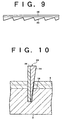
- FIG. 9 there is shown a combined filter and wedge array according to a third preferred embodiment of the present invention.
- the combined filter and wedge array is formed by vapor deposition of a dielectric multilayer film structure 26 of TiO 2 /SiO 2 , for example, on the array of wedge-shaped polyimide resin members 24 shown in FIG. 8C.
- a combined filter and wedge 28 as shown in FIG. 10 can be obtained. Accordingly, by inserting the combined filter and wedge 28 into the insertion groove 16, a structure similar to that shown in FIG. 3 can be easily provided in a single step.
- FIGS. 11A to 11C show a manufacturing process for a fourth preferred embodiment of the present invention.
- the opposite side surfaces of the SiO 2 cladding layer 4 are partially removed by etching to form triangular grooves 30 and 32.
- One side of each of the triangular grooves 30 and 32 is perpendicular to the corresponding side surface of the cladding layer 4.
- an insertion groove 34 is formed in such a manner that its one side coincides with one side of each of the triangular grooves 30 and 32. With this structure, the other side of the insertion groove 34 is made continuous between the cladding layer 4 and the silicon substrate 2 over the width thereof.
- the filter 18 is inserted into the insertion groove 34. Since the widths of the triangular grooves 30 and 32 are gradually increased toward the outside, the filter 18 can be easily inserted into the insertion groove 34 as being guided by the triangular groove 30 or 32. Further, two wedges 36 and 38 are substantially horizontally driven into the triangular grooves 30 and 32, respectively, from the outside thereof, thereby pressing the filter 18 on the continuous other side of the insertion groove 34 and accordingly maintaining the filter 18 substantially perpendicular to the optical waveguides 6 and 8 in a vertical plane.
- a wedge 44 is formed by first forming an SiO 2 layer 42 on an Si substrate 40 by CVD, for example, and next removing an unrequired portion of the SiO 2 layer 42 by etching.
- the wedge 44 can be driven into the triangular groove 30 by turning the condition shown in FIG. 12 upside down and next sliding the substrate 40 on the SiO 2 cladding layer 4.
- the shapes of the wide grooves are not limited to those shown, but any other shapes that can easily guide the filter may be adopted.
- the waveguide substrate is not limited to a silicon substrate, but any other substrates such as a glass substrate may be adopted.
- the optical waveguides may be formed of any other materials such as polymer.
- the present invention it is possible to provide a wavelength division multiplexing optical device which can facilitate a filter insertion step. Further, by driving a wedge into the insertion groove, the filter can be maintained substantially perpendicular to the optical waveguides, thereby reducing insertion loss of light.
Landscapes
- Physics & Mathematics (AREA)
- Engineering & Computer Science (AREA)
- Microelectronics & Electronic Packaging (AREA)
- General Physics & Mathematics (AREA)
- Optics & Photonics (AREA)
- Optical Integrated Circuits (AREA)
Description
- The present invention relates to a wavelength division multiplexing optical device and a manufacturing method therefor.
- The widespread use of a communication network using optical fiber transmission is indispensable to construct a multimedia information society. It is therefore necessary to realize a photodetection module capable of efficiently converting an optical signal into an electrical signal at a low cost. Further, wavelength division multiplexing optical communication for multiplexing light having different wavelengths by utilizing wavelength independence of light to transmit the resultant wavelength division multiplexed light is expected to provide various services including bidirectional communication and service multiplexing. It is therefore essential to use a wavelength division multiplexing optical device for multiplexing optical signals having different wavelengths and/or demultiplexing wavelength division multiplexed signal light.
- A conventional waveguide type wavelength division multiplexing optical device is described in Japanese Patent Laid-open No. 63-33707. In this conventional device, an optical waveguide having a Y branch portion is formed on a silicon substrate, and a groove is formed so as to extend across the Y branch portion. A dielectric multilayer film filter is inserted in this groove. This type wavelength division multiplexing optical device has a small size and good isolation characteristics, so that it is advantageous over a Mach-Zehnder type wavelength division multiplexing optical device and a fiber fusion splice type optical device.
- However, the above-mentioned wavelength division multiplexing optical device structure has a problem that insertion of the filter into the groove is difficult. That is, the filter film having a thickness of about 15 µm must be inserted into the groove having a width of about 25 µm, thus making the insertion difficult. Further, to suppress an increase in insertion loss, an error of tilt angle of the filter from a vertical direction must be suppressed within about 0.5° . Accordingly, it is difficult to stably fabricate a wavelength division multiplexing optical device in the conventional structure.
- It is therefore an object of the present invention to provide a wavelength division multiplexing optical device which can facilitate the insertion of the filter.
- It is another object of the present invention to provide a wavelength division multiplexing optical device which can reduce insertion loss of light by providing a structure capable of inserting and maintaining the filter in perpendicular relationship to a waveguide.
- In accordance with an aspect of the present invention, there is provided a wavelength division multiplexing optical device comprising a waveguide substrate; a cladding layer formed on said waveguide substrate, said cladding layer having first and second end surfaces and first and second side surfaces; a first optical waveguide embedded in said cladding layer; a second optical waveguide embedded in said cladding layer and connected at one end thereof to an intermediate portion of said first optical waveguide; an insertion groove formed in said waveguide substrate and said cladding layer between said first side surface and said second side surface so as to extend across a connected portion of said first and second optical waveguides; first and second wide grooves formed in at least said cladding layer so as to cover opposite end portions of said insertion groove and open to said first and second side surfaces of said cladding layer, respectively; and a wavelength selecting filter inserted in said insertion groove.
- Preferably, the widths of the first and second wide grooves are gradually increased toward the first and second side surfaces, respectively. More preferably, a wedge is driven into the insertion groove to press the wavelength selecting filter on a wall surface defining the insertion groove.
- In accordance with another aspect of the present invention, there is provided a manufacturing method for a wavelength division multiplexing optical device, comprising the steps of forming a first cladding layer on a waveguide substrate; forming a waveguide layer on said first cladding layer; etching said waveguide layer to form an optical waveguide having a Y branch portion; forming a second cladding layer on said first cladding layer so as to cover said optical waveguide; etching said first and second cladding layers to form first and second wide grooves respectively opening to opposite side surfaces of said first and second cladding layers; forming an insertion groove in said first and second cladding layers and said waveguide substrate so that said insertion groove extends across said Y branch portion of said optical waveguide along said first and second wide grooves; and inserting a wavelength selecting filter into said insertion groove.
- The first and second wide grooves may be replaced by first and second wide recesses formed on the opposite side surfaces of the waveguide substrate by cutting.
- The above and other objects, features and advantages of the present invention and the manner of realizing them will become more apparent, and the invention itself will best be understood from a study of the following description and appended claims with reference to the attached drawings showing some preferred embodiments of the invention.
-
- FIG. 1 is a perspective view of a first preferred embodiment of the present invention;
- FIG. 2 is a plan view of the first preferred embodiment;
- FIG. 3 is a cross section taken along the line 3-3 in FIG. 1;
- FIGS. 4A to 4D are plan views showing a manufacturing process for the first preferred embodiment of the present invention;
- FIGS. 5A to 5D are perspective views showing a forming process for optical waveguides;
- FIGS. 6A to 6D are views showing a manufacturing process for a second preferred embodiment of the present invention;
- FIGS. 7A and 7B are a plan view and an elevational view, respectively, showing another manufacturing method for wide grooves;
- FIGS. 8A to 8C are views showing a manufacturing process for wedges;
- FIG. 9 is a view showing a combined filter and wedge array;
- FIG. 10 is a sectional view of a third preferred embodiment of the present invention;
- FIGS. 11A to 11C are plan views showing a manufacturing process for a fourth preferred embodiment of the present invention; and
- FIG. 12 is a perspective view of a wedge usable in the fourth preferred embodiment.
-
- FIG. 1 is a perspective view of a wavelength division multiplexing optical device according to a first preferred embodiment of the present invention, and FIG. 2 is a plan view of the wavelength division multiplexing optical device shown in FIG. 1. An SiO2 cladding layer 4 is formed on a silicon (Si)
substrate 2. Thecladding layer 4 is formed by depositing a layer of SiO2 on theSi substrate 2 by CVD, for example. Thecladding layer 4 has first andsecond end surfaces second side surfaces 4c and 4d. - A first
optical waveguide 6 and a secondoptical waveguide 8 are embedded in thecladding layer 4. The first and secondoptical waveguides optical waveguide 6 and the secondoptical waveguide 8 are connected together at aY branch portion 10. The firstoptical waveguide 6 has afirst end surface 6a exposed to thefirst end surface 4a of thecladding layer 4 and asecond end surface 6b exposed to thesecond end surface 4b of thecladding layer 4. The secondoptical waveguide 8 has an end surface 8a exposed to thefirst end surface 4a of thecladding layer 4. - The
cladding layer 4 is formed with first and secondwide grooves second side surfaces 4c and 4d of thecladding layer 4. The first and secondwide grooves wide grooves second side surfaces 4c and 4d of thecladding layer 4, respectively. - An
insertion groove 16 is formed in theSi substrate 2 and the SiO2 cladding layer 4 so as to extend between the opposite side surfaces of theSi substrate 2 and pass across theY branch portion 10 of the first and secondoptical waveguides wide grooves insertion groove 16 is formed by using a dicing saw, for example, and has a width of about 25 µm. - A dielectric
multilayer film filter 18 is inserted in theinsertion groove 16. Since the widths of the first and secondwide grooves multilayer film filter 18 can be easily inserted into theinsertion groove 16 by first inserting thefilter 18 into one of thewide grooves filter 18 toward a central portion of theinsertion groove 16 where theY branch portion 10 of the first and secondoptical waveguides - Referring to FIG. 3, there is shown a cross section taken along the line 3-3 in FIG. 1. The width of the
insertion groove 16 is generally larger than the thickness of the dielectricmultilayer film filter 18. For example, theinsertion groove 16 has a width of about 25 µm, and the dielectricmultilayer film filter 18 has a thickness of about 15 µm. Accordingly, there is a possibility that the dielectricmultilayer film filter 18 formed by laminating a plurality ofdielectric films 18a on asubstrate 18b may be inclined to the first and secondoptical waveguides filter 18 is inserted in theinsertion groove 16. To eliminate this possibility, this preferred embodiment employs awedge 20 driven into theinsertion groove 16 to press the dielectricmultilayer film filter 18 on a vertical wall surface defining theinsertion groove 16. - Accordingly, the dielectric
multilayer film filter 18 can be positioned in substantially perpendicular relationship to theoptical waveguides wedge 20 is formed of a transparent material capable of transmitting light propagating in theoptical waveguides - Of signal light having wavelengths λ1 and λ2 entered the first
optical waveguide 6 from itsfirst end surface 6a, the signal light having the wavelength λ2 is passed through the dielectricmultilayer film filter 18 and emerged from thesecond end surface 6b of the firstoptical waveguide 6. On the other hand, the signal light having the wavelength λ1 is reflected by the dielectricmultilayer film filter 18, coupled to the secondoptical waveguide 8, and emerged from the end surface 8a of the secondoptical waveguide 8. For example, λ1 = 1.55 µm and λ2 = 1.3 µm. - While the two
wide grooves cladding layer 4 in the first preferred embodiment mentioned above, one wide groove may be formed so as to open to one of the opposite side surfaces 4c and 4d for the purpose of easy insertion of thefilter 18 into theinsertion groove 16. - A manufacturing process for the first preferred embodiment of the present invention will now be described with reference to FIGS. 4A to 4D. As shown in FIG. 4A, the first and second
optical waveguides optical waveguides Y branch portion 10. - This forming process for the
optical waveguides Si substrate 2 by CVD or sputtering, for example. As shown in FIG. 5B, an SiO2 layer doped with TiO2 as awaveguide layer 5 is next formed on thefirst cladding layer 3 by CVD or sputtering, for example. As shown in FIG. 5C, an unrequired portion of thewaveguide layer 5 is next removed by etching to form the first and secondoptical waveguides first cladding layer 3 so as to cover the first and secondoptical waveguides - Referring back to FIG. 4B, the opposite side surfaces of the SiO2 cladding layer 4 are partially removed by reactive ion etching, for example, at a position where the
insertion groove 16 is to be formed later, thereby forming thewide grooves insertion groove 16 for receiving the dielectricmultilayer film filter 18 is next formed by using a dicing saw or the like in such a manner as to extend across theY branch portion 10 along thewide grooves - As shown in FIG. 4D, the dielectric
multilayer film filter 18 is finally inserted into theinsertion groove 16 by utilizing one of thewide grooves wedge 20 may be driven into theinsertion groove 16 after the step shown in FIG. 4D. - Referring to FIGS. 6A to 6D, there is shown a manufacturing process for a second preferred embodiment of the present invention. This manufacturing process is different from the manufacturing process for the first preferred embodiment shown in FIG. 4A to 4D in the step of forming a wide groove or recess shown in FIG. 6B. The other steps are similar to those of the manufacturing process for the first preferred embodiment. In the manufacturing process for the second preferred embodiment, as shown in FIG. 6B, a plurality of
waveguide substrates 2 withcladding layers 4 each formed withoptical waveguides waveguide substrates 2 withcladding layers 4 by using a dicing saw or the like. Similarly, a plurality of grooves or recesses 12a are formed on the other same side surfaces of thewaveguide substrates 2 with cladding layers 4. - FIGS. 7A and 7B are a plan view and an elevational view, respectively, showing another manufacturing method for the wide grooves. In this manufacturing method, wide V-shaped
grooves silicon substrate 2. By setting the crystal orientation of thesilicon substrate 2 as shown in FIG. 7A and carrying out anisotropic etching using KOH, the (111) plane of thesilicon substrate 2 can be exposed into the V-shapedgrooves - FIGS. 8A to 8C show a manufacturing process for the wedge. As shown in FIG. 8A, a sawtooth structure as a mold is first formed on a
substrate 22 by cutting or etching, and apolyimide solution 24 is next applied to the sawtooth structure. Thepolyimide solution 24 is next cured to form an array of wedge-shapedpolyimide resin members 24 connected together as shown in FIG. 8B. Theseconnected resin members 24 are next cut alonglines 25 shown in FIG. 8C to obtain a plurality ofindividual wedges 20 as shown in FIG. 3. - Referring to FIG. 9, there is shown a combined filter and wedge array according to a third preferred embodiment of the present invention. The combined filter and wedge array is formed by vapor deposition of a dielectric
multilayer film structure 26 of TiO2/SiO2, for example, on the array of wedge-shapedpolyimide resin members 24 shown in FIG. 8C. By cutting the combined filter and wedge array obtained above into individual pieces along lines similar to thelines 25 shown in FIG. 8C, a combined filter andwedge 28 as shown in FIG. 10 can be obtained. Accordingly, by inserting the combined filter andwedge 28 into theinsertion groove 16, a structure similar to that shown in FIG. 3 can be easily provided in a single step. - FIGS. 11A to 11C show a manufacturing process for a fourth preferred embodiment of the present invention. As shown in FIG. 11A, the opposite side surfaces of the SiO2 cladding layer 4 are partially removed by etching to form
triangular grooves triangular grooves cladding layer 4. As shown in FIG. 11B, aninsertion groove 34 is formed in such a manner that its one side coincides with one side of each of thetriangular grooves insertion groove 34 is made continuous between thecladding layer 4 and thesilicon substrate 2 over the width thereof. - As shown in FIG. 11C, the
filter 18 is inserted into theinsertion groove 34. Since the widths of thetriangular grooves filter 18 can be easily inserted into theinsertion groove 34 as being guided by thetriangular groove wedges triangular grooves filter 18 on the continuous other side of theinsertion groove 34 and accordingly maintaining thefilter 18 substantially perpendicular to theoptical waveguides - An example of
such wedges wedge 44 is formed by first forming an SiO2 layer 42 on anSi substrate 40 by CVD, for example, and next removing an unrequired portion of the SiO2 layer 42 by etching. Thewedge 44 can be driven into thetriangular groove 30 by turning the condition shown in FIG. 12 upside down and next sliding thesubstrate 40 on the SiO2 cladding layer 4. - Having thus described various preferred embodiments of the present invention, the shapes of the wide grooves are not limited to those shown, but any other shapes that can easily guide the filter may be adopted. Further, the waveguide substrate is not limited to a silicon substrate, but any other substrates such as a glass substrate may be adopted. In addition, the optical waveguides may be formed of any other materials such as polymer.
- According to the present invention, it is possible to provide a wavelength division multiplexing optical device which can facilitate a filter insertion step. Further, by driving a wedge into the insertion groove, the filter can be maintained substantially perpendicular to the optical waveguides, thereby reducing insertion loss of light.
Claims (13)
- A wavelength division multiplexing optical device comprising:characterized in that first and second grooves (12, 14) are formed in at least said cladding layer, the first and second grooves being wider than the insertion groove so as to cover opposite end portions of said insertion groove and open to said first and second side surfaces of said cladding layer, respectively.a waveguide substrate (2);a cladding layer (4) formed on said waveguide substrate (2), said cladding layer having first and second end surfaces (4a, 4b) and first and second side surfaces (4c, 4d);a first optical waveguide (6) embedded in said cladding layer;a second optical waveguide (8) embedded in said cladding layer and connected at one end thereof to an intermediate portion of said first optical waveguide;an insertion groove (16) formed in said waveguide substrate and said cladding layer between said first side surface and said second side surface so as to extend across a connected portion of said first and second optical waveguides;a wavelength selecting filter (18) inserted in said insertion groove.
- A wavelength division multiplexing optical device according to claim 1, wherein the widths of said first and second wide grooves are gradually increased toward said first and second side surfaces, respectively.
- A wavelength division multiplexing optical device according to claim 1, wherein said first and second wide grooves are formed by etching.
- A wavelength division multiplexing optical device according to claim 1, wherein said first and second wide grooves are formed by cutting said cladding layer and said waveguide substrate.
- A wavelength division multiplexing optical device according to claim 1, further comprising a wedge driven into said insertion groove, for pressing said wavelength selecting filter on a wall surface of said insertion groove.
- A wavelength division multiplexing optical device according to claim 1, wherein said wavelength selecting filter is wedge-shaped.
- A wavelength division multiplexing optical device according to claim 1, wherein said first and second wide grooves are triangular, and said device further comprises first and second wedges substantially horizontally driven into said first and second wide grooves from said first and second side surfaces, respectively, for pressing said wavelength selecting filter on a wall surface of said insertion groove.
- A wavelength division multiplexing optical device comprising:characterized in that a groove is formed in at least said cladding layer, said groove being wider than the insertion groove so as to cover one end portion of said insertion groove and open to one of said first and second side surfaces.a waveguide substrate (2),a cladding layer (4) formed on said waveguide substrate (2), said cladding layer having first and second end surfaces (4a, 4b) and first and second side surfaces (4c, 4d);a first optical waveguide (6) embedded in said cladding layer;a second optical waveguide (8) embedded in said cladding layer and connected at one end thereof to an intermediate portion of said first optical waveguide;an insertion groove (16) formed in said waveguide substrate and said cladding layer between said first side surface and said second side surface so as to extend across a connected portion of said first and second optical waveguides;a wavelength selecting filter inserted in said insertion groove.
- A wavelength division multiplexing optical device according to claim 8, wherein the width of said wide groove is gradually increased toward said one of said first and second side surfaces.
- A manufacturing method for a wavelength division multiplexing optical device, comprising the steps of:forming a first cladding layer (3) on a waveguide substrate (2);forming a waveguide layer (5) on said first cladding layer;etching said waveguide layer to form an optical waveguide having a Y branch portion;forming a second cladding layer (7) on said first cladding layer so as to cover said optical waveguide;etching said first and second cladding layers to form first and second grooves (12a, 14a) respectively opening to opposite side surfaces of said first and second cladding layers;forming an insertion groove (16) in said first and second cladding layers and said waveguide substrate so that said insertion groove extends across said Y branch portion of said optical waveguide along said first and second wide grooves said insertion groove being narrower than said first and second grooves; andinserting a wavelength selecting filter into said insertion groove.
- A manufacturing method according to claim 10, further comprising the step of driving a wedge into said insertion groove.
- A manufacturing method for a wavelength division multiplexing optical device, comprising the steps of:forming a first cladding layer (3) on a waveguide substrate (2);forming a waveguide layer on said first cladding layer;etching said waveguide layer (5) to form an optical waveguide having a Y branch portion;forming a second cladding layer (7) on said first cladding layer so as to cover said optical waveguide;cutting opposite side surfaces of said waveguide substrate to form first and second recesses;forming an insertion groove (16) in said first and second cladding layers and said waveguide substrate so that said insertion groove extends across said Y branch portion of said optical waveguide between said first and second recesses said insertion groove being narrower than said first and second recesses; andinserting a wavelength selecting filter into said insertion groove.
- A manufacturing method according to claim 12, further comprising the step of driving a wedge into said insertion groove.
Applications Claiming Priority (3)
| Application Number | Priority Date | Filing Date | Title |
|---|---|---|---|
| JP27273397A JP3708306B2 (en) | 1997-10-06 | 1997-10-06 | Wavelength division multiplexing optical device and manufacturing method thereof |
| JP272733/97 | 1997-10-06 | ||
| JP27273397 | 1997-10-06 |
Publications (3)
| Publication Number | Publication Date |
|---|---|
| EP0908746A2 EP0908746A2 (en) | 1999-04-14 |
| EP0908746A3 EP0908746A3 (en) | 2000-02-23 |
| EP0908746B1 true EP0908746B1 (en) | 2004-05-19 |
Family
ID=17518029
Family Applications (1)
| Application Number | Title | Priority Date | Filing Date |
|---|---|---|---|
| EP98105113A Expired - Lifetime EP0908746B1 (en) | 1997-10-06 | 1998-03-20 | Wavelength division multiplexing optical device and manufacturing method therefor |
Country Status (4)
| Country | Link |
|---|---|
| US (1) | US6085000A (en) |
| EP (1) | EP0908746B1 (en) |
| JP (1) | JP3708306B2 (en) |
| DE (1) | DE69823948D1 (en) |
Families Citing this family (30)
| Publication number | Priority date | Publication date | Assignee | Title |
|---|---|---|---|---|
| US6219470B1 (en) * | 1999-09-23 | 2001-04-17 | Xiang Zheng Tu | Wavelength division multiplexing transmitter and receiver module |
| JP2001108847A (en) * | 1999-10-07 | 2001-04-20 | Mitsubishi Electric Corp | Optical module |
| JP2001305357A (en) * | 2000-04-19 | 2001-10-31 | Oki Electric Ind Co Ltd | Wavelength demultiplexer |
| JP2002214460A (en) * | 2001-01-19 | 2002-07-31 | Japan Aviation Electronics Industry Ltd | Optical waveguide device and method of manufacturing the same |
| JP2003021723A (en) * | 2001-07-06 | 2003-01-24 | Photonixnet Corp | Mode cut filter and optical transmitter-receiver |
| JP2003114334A (en) * | 2001-10-04 | 2003-04-18 | Matsushita Electric Ind Co Ltd | Optical filter module and method of manufacturing the same |
| JP2003114335A (en) * | 2001-10-04 | 2003-04-18 | Matsushita Electric Ind Co Ltd | Optical filter module and method of manufacturing the same |
| JP2003114336A (en) * | 2001-10-04 | 2003-04-18 | Matsushita Electric Ind Co Ltd | Optical filter module and method of manufacturing the same |
| US7123798B2 (en) | 2002-03-29 | 2006-10-17 | Ngk Insulators, Ltd. | Optical device and method of producing the same |
| JP2004053868A (en) * | 2002-07-19 | 2004-02-19 | Yutaka Katsuyama | Optical module |
| JP2004053869A (en) * | 2002-07-19 | 2004-02-19 | Yutaka Katsuyama | Optical network system that can easily increase or decrease the number of terminals |
| JP4012785B2 (en) * | 2002-08-27 | 2007-11-21 | 日本板硝子株式会社 | Optical connection device |
| EP1426799A3 (en) | 2002-11-29 | 2005-05-18 | Matsushita Electric Industrial Co., Ltd. | Optical demultiplexer, optical multi-/demultiplexer, and optical device |
| US7195402B2 (en) | 2002-12-20 | 2007-03-27 | Ngk Insulators, Ltd. | Optical device |
| US7308174B2 (en) * | 2002-12-20 | 2007-12-11 | Ngk Insulators, Ltd. | Optical device including a filter member for dividing a portion of signal light |
| WO2004057397A1 (en) | 2002-12-20 | 2004-07-08 | Ngk Insulators, Ltd. | Optical device |
| US7321703B2 (en) | 2002-12-20 | 2008-01-22 | Ngk Insulators, Ltd. | Optical device |
| JP2004309530A (en) * | 2003-04-02 | 2004-11-04 | Yutaka Katsuyama | Optical signal controller |
| JP4031804B2 (en) | 2003-06-02 | 2008-01-09 | 日本碍子株式会社 | Optical device |
| US7313297B2 (en) * | 2003-09-12 | 2007-12-25 | Nippon Telegraph And Telephone Corporation | Wavelength multi/demultiplexer |
| JP2005195615A (en) * | 2003-12-26 | 2005-07-21 | Matsushita Electric Ind Co Ltd | Optical waveguide substrate, optical transceiver module and optical transmission device |
| KR100630091B1 (en) * | 2004-10-29 | 2006-09-27 | 삼성전자주식회사 | Optical filter and manufacturing method of optical filter and planar waveguide device using same |
| JP4509892B2 (en) * | 2005-08-26 | 2010-07-21 | 浜松ホトニクス株式会社 | Optical waveguide substrate and manufacturing method thereof |
| JP4780532B2 (en) | 2005-11-18 | 2011-09-28 | 日立化成工業株式会社 | Optical device |
| JP2007272054A (en) * | 2006-03-31 | 2007-10-18 | Hitachi Chem Co Ltd | Optical waveguide structure |
| JP4582136B2 (en) * | 2007-10-03 | 2010-11-17 | 日本電気株式会社 | Optical waveguide device and manufacturing method thereof |
| JP2010060950A (en) * | 2008-09-05 | 2010-03-18 | Hitachi Ltd | Optical module mounted with wdm filter and manufacturing method |
| US7991251B2 (en) * | 2008-07-02 | 2011-08-02 | Hitachi, Ltd. | Optical module mounted with WDM filter |
| CN103609048B (en) * | 2013-06-24 | 2016-08-31 | 华为技术有限公司 | A kind of optical module and optical network system |
| JP6219887B2 (en) * | 2015-06-25 | 2017-10-25 | Nttエレクトロニクス株式会社 | Optical waveguide device |
Family Cites Families (10)
| Publication number | Priority date | Publication date | Assignee | Title |
|---|---|---|---|---|
| JPS61282803A (en) * | 1985-06-07 | 1986-12-13 | Matsushita Electric Ind Co Ltd | Optical multiplexing/demultiplexing device |
| US4790615A (en) * | 1986-03-06 | 1988-12-13 | Nippon Sheet Glass Co., Ltd. | Demultiplexing and/or multiplexing optical circuit |
| JPS6333707A (en) * | 1986-07-28 | 1988-02-13 | Nippon Telegr & Teleph Corp <Ntt> | Waveguide type optical multiplexer/demultiplexer |
| GB2245080B (en) * | 1990-06-16 | 1993-11-10 | Gec Ferranti Defence Syst | Fibre optic waveguide coupler |
| JP2752848B2 (en) * | 1992-05-29 | 1998-05-18 | 日本電信電話株式会社 | Manufacturing method of optical waveguide with interference filter |
| JPH07318751A (en) * | 1994-05-25 | 1995-12-08 | Furukawa Electric Co Ltd:The | Optical waveguide module |
| TW323341B (en) * | 1995-01-09 | 1997-12-21 | Minnesota Mining & Mfg | |
| JPH08271742A (en) * | 1995-04-03 | 1996-10-18 | Hitachi Cable Ltd | Method of manufacturing waveguide with filter and block for fixing filter |
| JPH0921912A (en) * | 1995-07-05 | 1997-01-21 | Furukawa Electric Co Ltd:The | Dielectric multilayer filter, manufacturing method thereof, and structure for inserting dielectric multilayer filter into optical waveguide |
| JPH0961664A (en) * | 1995-08-21 | 1997-03-07 | Fujitsu Ltd | Optical transmission equipment parts |
-
1997
- 1997-10-06 JP JP27273397A patent/JP3708306B2/en not_active Expired - Fee Related
-
1998
- 1998-03-13 US US09/041,731 patent/US6085000A/en not_active Expired - Lifetime
- 1998-03-20 EP EP98105113A patent/EP0908746B1/en not_active Expired - Lifetime
- 1998-03-20 DE DE69823948T patent/DE69823948D1/en not_active Expired - Lifetime
Also Published As
| Publication number | Publication date |
|---|---|
| US6085000A (en) | 2000-07-04 |
| DE69823948D1 (en) | 2004-06-24 |
| EP0908746A2 (en) | 1999-04-14 |
| EP0908746A3 (en) | 2000-02-23 |
| JP3708306B2 (en) | 2005-10-19 |
| JPH11109149A (en) | 1999-04-23 |
Similar Documents
| Publication | Publication Date | Title |
|---|---|---|
| US6085000A (en) | Wavelength division multiplexing optical device and manufacturing method therefor | |
| EP0938000B1 (en) | Optical waveguide branch with reflector | |
| US8639073B2 (en) | Fiber coupling technique on a waveguide | |
| KR100897887B1 (en) | Hybrid Integrated Structure of Planar Optical Waveguide Device and Active Device Using Fiber Array | |
| KR100630804B1 (en) | Multiwavelength Optical Transceiver Module, Multiplex and Demultiplexer Using Thin Film Filter | |
| JP3344446B2 (en) | Optical transceiver module | |
| US4589724A (en) | Multiple branching light wave guide element | |
| US20240061180A1 (en) | Wavelength division multiplexing/demultiplexing devices | |
| JP2921877B2 (en) | Waveguide demultiplexing module and method of manufacturing the same | |
| JPH09105824A (en) | Waveguide type optical element | |
| JP3246710B2 (en) | Optical device manufacturing method | |
| US6574390B2 (en) | Configuration to multiplex and/or demultiplex the signals of a plurality of optical data channels and method for the production of the configuration | |
| EP1496377A2 (en) | Optical multiplexer/demultiplexer, optical integrated circuit and light transceiver using the same | |
| JP2000131543A (en) | Optical transmission and reception module and its manufacture | |
| US6104847A (en) | Optical device having an optical waveguide structure | |
| JP3357979B2 (en) | Optical wavelength multiplexer / demultiplexer | |
| WO2004029681A1 (en) | Integrated optical device | |
| JP3737821B2 (en) | Wavelength division device | |
| JP2744309B2 (en) | Coupling structure of optical waveguide and light receiving element | |
| KR100403740B1 (en) | Optical fiber array equipment structure | |
| JP3487730B2 (en) | Array waveguide grating element | |
| JPH10260437A (en) | Nonlinear optical coupler | |
| JPH10133041A (en) | Waveguide with filter | |
| JP2010060653A (en) | Optical device and optical signal selection method | |
| JP3600975B2 (en) | 2-wavelength optical multiplexer / demultiplexer |
Legal Events
| Date | Code | Title | Description |
|---|---|---|---|
| PUAI | Public reference made under article 153(3) epc to a published international application that has entered the european phase |
Free format text: ORIGINAL CODE: 0009012 |
|
| AK | Designated contracting states |
Kind code of ref document: A2 Designated state(s): DE GB |
|
| AX | Request for extension of the european patent |
Free format text: AL;LT;LV;MK;RO;SI |
|
| PUAL | Search report despatched |
Free format text: ORIGINAL CODE: 0009013 |
|
| AK | Designated contracting states |
Kind code of ref document: A3 Designated state(s): AT BE CH DE DK ES FI FR GB GR IE IT LI LU MC NL PT SE |
|
| AX | Request for extension of the european patent |
Free format text: AL;LT;LV;MK;RO;SI |
|
| 17P | Request for examination filed |
Effective date: 20000222 |
|
| AKX | Designation fees paid |
Free format text: DE GB |
|
| GRAP | Despatch of communication of intention to grant a patent |
Free format text: ORIGINAL CODE: EPIDOSNIGR1 |
|
| GRAS | Grant fee paid |
Free format text: ORIGINAL CODE: EPIDOSNIGR3 |
|
| GRAA | (expected) grant |
Free format text: ORIGINAL CODE: 0009210 |
|
| AK | Designated contracting states |
Kind code of ref document: B1 Designated state(s): DE GB |
|
| REG | Reference to a national code |
Ref country code: GB Ref legal event code: FG4D |
|
| REF | Corresponds to: |
Ref document number: 69823948 Country of ref document: DE Date of ref document: 20040624 Kind code of ref document: P |
|
| PG25 | Lapsed in a contracting state [announced via postgrant information from national office to epo] |
Ref country code: DE Free format text: LAPSE BECAUSE OF FAILURE TO SUBMIT A TRANSLATION OF THE DESCRIPTION OR TO PAY THE FEE WITHIN THE PRESCRIBED TIME-LIMIT Effective date: 20040820 |
|
| PLBE | No opposition filed within time limit |
Free format text: ORIGINAL CODE: 0009261 |
|
| STAA | Information on the status of an ep patent application or granted ep patent |
Free format text: STATUS: NO OPPOSITION FILED WITHIN TIME LIMIT |
|
| 26N | No opposition filed |
Effective date: 20050222 |
|
| PGFP | Annual fee paid to national office [announced via postgrant information from national office to epo] |
Ref country code: GB Payment date: 20130320 Year of fee payment: 16 |
|
| GBPC | Gb: european patent ceased through non-payment of renewal fee |
Effective date: 20140320 |
|
| PG25 | Lapsed in a contracting state [announced via postgrant information from national office to epo] |
Ref country code: GB Free format text: LAPSE BECAUSE OF NON-PAYMENT OF DUE FEES Effective date: 20140320 |