EP0904576B1 - Power supply circuit - Google Patents
Power supply circuit Download PDFInfo
- Publication number
- EP0904576B1 EP0904576B1 EP98916836A EP98916836A EP0904576B1 EP 0904576 B1 EP0904576 B1 EP 0904576B1 EP 98916836 A EP98916836 A EP 98916836A EP 98916836 A EP98916836 A EP 98916836A EP 0904576 B1 EP0904576 B1 EP 0904576B1
- Authority
- EP
- European Patent Office
- Prior art keywords
- power supply
- supply circuit
- voltage
- current
- output
- Prior art date
- Legal status (The legal status is an assumption and is not a legal conclusion. Google has not performed a legal analysis and makes no representation as to the accuracy of the status listed.)
- Expired - Lifetime
Links
Images
Classifications
-
- G—PHYSICS
- G05—CONTROLLING; REGULATING
- G05F—SYSTEMS FOR REGULATING ELECTRIC OR MAGNETIC VARIABLES
- G05F1/00—Automatic systems in which deviations of an electric quantity from one or more predetermined values are detected at the output of the system and fed back to a device within the system to restore the detected quantity to its predetermined value or values, i.e. retroactive systems
- G05F1/10—Regulating voltage or current
- G05F1/46—Regulating voltage or current wherein the variable actually regulated by the final control device is DC
- G05F1/56—Regulating voltage or current wherein the variable actually regulated by the final control device is DC using semiconductor devices in series with the load as final control devices
- G05F1/59—Regulating voltage or current wherein the variable actually regulated by the final control device is DC using semiconductor devices in series with the load as final control devices including plural semiconductor devices as final control devices for a single load
-
- G—PHYSICS
- G05—CONTROLLING; REGULATING
- G05F—SYSTEMS FOR REGULATING ELECTRIC OR MAGNETIC VARIABLES
- G05F3/00—Non-retroactive systems for regulating electric variables by using an uncontrolled element, or an uncontrolled combination of elements, such element or such combination having self-regulating properties
- G05F3/02—Regulating voltage or current
- G05F3/08—Regulating voltage or current wherein the variable is DC
- G05F3/10—Regulating voltage or current wherein the variable is DC using uncontrolled devices with non-linear characteristics
- G05F3/16—Regulating voltage or current wherein the variable is DC using uncontrolled devices with non-linear characteristics being semiconductor devices
- G05F3/20—Regulating voltage or current wherein the variable is DC using uncontrolled devices with non-linear characteristics being semiconductor devices using diode- transistor combinations
- G05F3/26—Current mirrors
-
- H—ELECTRICITY
- H02—GENERATION; CONVERSION OR DISTRIBUTION OF ELECTRIC POWER
- H02J—ELECTRIC POWER NETWORKS; CIRCUIT ARRANGEMENTS OR SYSTEMS FOR SUPPLYING OR DISTRIBUTING ELECTRIC POWER; SYSTEMS FOR STORING ELECTRIC ENERGY
- H02J1/00—Circuit arrangements for DC mains or DC distribution networks
- H02J1/10—Parallel operation of DC sources
- H02J1/108—Parallel operation of DC sources having arrangements for blocking reverse current flow, e.g. using diodes
Definitions
- the invention is based on a power supply circuit according to the genre of independent claims.
- the Power supply circuit is said to be on several Input voltage sources that are operated can have different voltages.
- the Input voltage sources cannot be used easily be interconnected.
- a usual measure therefore sees the use of decoupling diodes, so that the Input voltage source that has the higher voltage is connected to the further circuit while the Input voltage source with the lower voltage is uncoupled.
- the disadvantage of this known solution is it that the at least occurring voltage difference between an output of the power supply circuit and the Input voltage source around the forward voltage of a diode in addition to that in the power supply circuit anyway occurring voltage difference is increased.
- the invention has for its object a Specify power supply circuit consisting of at least two different input voltage sources can be supplied can, the smallest possible voltage difference between the output of the power supply circuit and the Input voltage source with the highest voltage occur should.
- the different versions of the invention Power supply circuit is common to everyone Input voltage source a current mirror is connected the current provided by a power source Control input of an output transistor available provides. With this measure, the control voltage of the Output transistor close to the voltage of the reach the relevant input voltage source.
- the Voltage difference can range from just 0.1 to 0.3 volts lie that the saturation voltage of a collector-emitter path of a transistor contained in the current mirror equivalent.
- a current mirror poses at one Output current connector has a maximum current ready at an input power connection is specified.
- the Gear ratio can be freely selected.
- a major advantage is that between the in the input current connection and the current flowing from the Output current connection out flowing current Potential difference.
- the current mirror is on to connect a power supply connection in the The currents appearing in the current mirror must be able to provide, the voltage at Power supply connection determines the potential relationships.
- Circuit are the at least two input voltage sources about those known from the prior art Decoupling diodes on an output transistor connected together.
- a reduction in the occurrence Voltage drop still results from connecting the Current level directly at the input voltage source, so that in addition to the voltage drop across the Decoupling diodes occurs, only a small one Voltage drop at the output transistor accepted must become.
- the voltage drop across the output transistor is by the saturation voltage of the emitter-collector path certainly.
- Power supply circuit is any input voltage source assigned an output transistor.
- the output transistors are at the output of the power supply circuit connected together.
- the output transistors take care of that required decoupling of the input voltage sources.
- the power supply circuit according to the invention Execution allows a particularly low Voltage difference between that at the output of the Power supply circuit lying voltage and the Input voltage source with the highest voltage. By the Eliminating the decoupling diodes reduces the minimum Voltage difference on the forward voltage of the Output transistors.
- a first advantageous Design provides that a single power source in the power supply circuit according to the invention is included, the a given current available to the current mirror provides. This measure is an inexpensive one Realization possible. Furthermore, the maximum current that can deliver the power supply circuit according to the invention, by the current provided by the power source, the Current displacement ratio of the current mirror and the Current gain factor of the output transistor set.
- the voltage supply circuit can by circuitry measures made short-circuit proof become. For this purpose, the current is usually recorded. If the current exceeds a predetermined maximum value, an additional circuit section reduces the current at Output the current mirror. The current consumption is independent on the number of actually switched on Input voltage sources.
- Another advantageous embodiment provides that the Output voltage is set to a predetermined value.
- a simple stabilization of the output voltage is through a parenthesis of the control input of the output transistor possible at a given potential.
- Suitable is preferably a limiter diode.
- An advantageous one Training this measure sees a closed Control circuit before, the output voltage with a Compares reference voltage. With this measure is one stable output voltage achievable.
- Power supply circuit required decoupling diodes are preferably implemented as bipolar diodes, the one have high reliability.
- Another configuration concerns the realization of the output transistors that preferably have an NPN structure. With this Measure is a simple integration of the Output transistors with the other electronic Components possible on a silicon chip.
- a preferred use of the invention Power supply circuit is in a motor vehicle given.
- aspirations take place instead of a single vehicle electrical system voltage, which is usually 12 V or 24 V is several different vehicle electrical system voltages provided.
- a modern Motor vehicle built numerous electronic devices that already contain power supply circuits that are in the used in the present case as input voltage sources can be.
- FIGS 1 to 4 show circuit diagrams of different Embodiments of an inventive Power supply circuit.
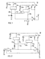
- Figure 1 shows a power supply circuit 10 which provides an output voltage to an output 11.
- the Input voltage of the power supply circuit 10 is from various input voltage sources are provided. in the shown embodiment are a first Input voltage source 12a and a second Input voltage source 12b shown via a first Decoupling diode 13a and a second decoupling diode 13b merged at a common output transistor 14 are.
- the common output transistor 14 is connected to the Output 11 connected.
- a first current mirror 15a, the Power connector 16a with the first Input voltage source 12a is connected Control input 17 of the common output transistor 14 a current available from a current source 18 is specified.
- the first current mirror 15a is therefore included its output current connection 19a with the control input 17th connected.
- the control input 17 of the common output transistor 14 is still one with an output power connector 19b connected second current mirror 15b, the Power connector 16b on the second Input voltage source 12b is connected.
- the two current mirrors 15a, 16b are with their Input power connections 20a, 20b each with the Power source 18 connected.
- the control input 17 of the common output transistor 14 is against a common voltage limiter 21 Circuit ground 22 switched.
- the power supply circuit 10 shown in FIG. 1 works as follows:
- the power supply circuit 10 provides an output 10 Tension ready either from the first or the second input voltage source 12a, 12b is obtained.
- the two input voltage sources 12a, 12b are via the two decoupling diodes 13a, 13b on the common Output transistor 14 interconnected and form one analog OR operation. With the output transistor 14 is therefore the input voltage source 12a, 12b connected, the at the polarity entered in Figure 1 Decoupling diodes 13a, 13b the higher voltage provides.
- each Input voltage source 12a, 12b is with a separate Current mirror 15a, 15b over the respective Input power connector 16a, 16b connected.
- the current mirror 15a, 15b delivers to the control input 17 of the common Output transistor 14 a current from the current source 18 is specified.
- the current mirror 15a, 15b, the detailed circuit implementation of the aforementioned Literature can be taken reflects the through the input current connection 20a, 20b in the current mirror 15a, 15b current flowing into the output current connection 19a, 19b, the transmission ratio being freely selectable.
- the maximum current flowing into the control input 17 of the common Output transistor 14 can flow is therefore through the Current of the current source 18 and through the set Gear ratio fixed. Depending on Current amplification factor of the common output transistor 14 the maximum current is fixed, which the output 11th can be removed.
- the invention Power supply circuit 10 is short-circuit proof.
- the main advantage of controlling the common Brings output transistor 14 with the current mirror 15a, 15b, is that the control input 17 of the common Output transistor 14 provided current may have different potential than that of the power source 18 delivered electricity.
- the input voltage source 12a, 12b has the potential at Control input 17 of the common output transistor 14 only slightly below the voltage of the Input voltage source 12a, 12b.
- the voltage difference is from the circuitry realization of the current mirror 15a, 15b dependent. With a realization according to the previously the mentioned reference corresponds to the voltage difference a saturation voltage of a collector-emitter path of a transistor, which are in the range of 0.1 V to 0.3 V. can. In addition to this voltage difference Voltage difference added between the Control input 17 of the common output transistor 14 and the output 11 occurs. When the common output transistor 14 in silicon technology must a voltage difference of about 0.7 V is added become.
- Another voltage drop occurs at the decoupling diodes 13a, 13b, which depends on the implementation of the diodes. If bipolar silicon diodes are used, the additional voltage drop at the decoupling diodes 13a, 13b up to 1 V. But compared to the previously known State of the art the potential at the control input 17 of the common output transistor 14 is significantly increased, overall there is a lower voltage difference than so far it could be achieved.
- the voltage at output 11 can with the common Voltage limiter 21 are set, the potential at the control input 17 of the common output transistor 14 sets.
- a limiter diode is suitable, for example a zener diode.
- FIG. 2 shows a development of the invention Power supply circuit 10 according to Figure 1.
- Voltage limiters 21 are a voltage divider 23, a Reference voltage source 24 and a comparator 25 intended.
- the voltage divider 23 and the Reference voltage source 24 are each with the comparator 25 connected, the output of which is connected to the control input 17 of the common output transistor 14 is connected.
- Power supply circuit 10 enables further training according to FIG. 2, regulation of the output 11 provided voltage of the power supply circuit 10 to a constant value, that of the Reference voltage source 24 is set. There is one closed control loop, so that depending on the Wiring the comparator 25 a high voltage stability can be achieved.
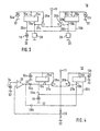
- FIG. 3 shows another embodiment of the invention Power supply circuit 10.
- the first output transistor 26a is immediately at the first input voltage source 12a connected and the second output transistor 26b immediately at the second input voltage source 12b connected. Both output transistors 26a, 26b are with connected to the output 11.
- a control input 27a of the first output transistor 26a is both with the first current mirror 15a above it Output current connection 19a as well as with a first one Voltage limiter 28 connected to the circuit ground 22 is connected.
- a control input 27b of the second Output transistor 26b is connected to both the second Current mirror 15b via its output current connection 19b as also connected to a second voltage limiter 29, the is connected to the circuit ground 22.
- the main difference between that in Figure 1 and the 3 shown in FIG The power supply circuit 10 according to the invention is that the achievable minimum voltage difference between the Voltage at output 11 and the higher voltage one of the Input voltage sources 12a, 12b according to the embodiment according to Figure 3 is again less than according to the Embodiment according to Figure 1. This is achieved by Elimination of the voltage drop at the decoupling diodes 13a, 13b inevitably occurs according to FIG. 1.
- the Decoupling of the input voltage sources 12a, 12b is through the use of the first and second output transistors 26a, 26b possible. Each input voltage source 12a, 12b receives therefore their own output transistor, all Transistors 26a, 26b are connected to the output 11.
- the voltage at the output 11 is determined by Bracketing of the control inputs 27a, 27b Output transistors 26a, 26b to predetermined values by means of of the two voltage limiters 28, 29 possible.
- the voltage limiters 28, 29 specify the same voltage.
- the between the output 11 and the input voltage source 12a, 12b occurring voltage difference is only from the voltage difference occurring in the current mirror 15a, 16b and of the between the control input 27a, 27b of the Output transistors 26a, 26b and the output 11 lying Voltage difference determined.
- the Output transistor 26a, 26b between the output 11 and the Input voltage source 12a, 12b occurring Voltage difference is negligible and therefore does not increase the total voltage difference.
- FIG. 4 shows a further development of that shown in FIG. 3 power supply circuit according to the invention 10.
- Power supply circuit 10 according to the invention are there included voltage limiter 28, 29 replaced by the Figure 2 known voltage divider 23, the Reference voltage source 24 and the comparator 25.
- voltage limiter 28 replaced by the Figure 2 known voltage divider 23, the Reference voltage source 24 and the comparator 25.
- Da compared to the embodiment shown in Figure 2 separate output transistors 26a, 26b are now provided are a first further decoupling diode 30a and another second decoupling diode 30b is required.
- the first further decoupling diode 30a connects the Comparator 25 with the control terminal 27a of the first Output transistor 26a and the second further Decoupling diode 30b connects the comparator 25 to the Control input 27b of the second output transistor 26b.
- 29 is according to the Development according to Figure 4 a regulation of the voltage on Output 11 to that determined by the reference voltage 24 Value possible.
- the resulting closed loop can be designed with regard to the desired control quality and enables a high constant voltage at the output 11th
Landscapes
- Engineering & Computer Science (AREA)
- Physics & Mathematics (AREA)
- Electromagnetism (AREA)
- General Physics & Mathematics (AREA)
- Radar, Positioning & Navigation (AREA)
- Automation & Control Theory (AREA)
- Microelectronics & Electronic Packaging (AREA)
- Nonlinear Science (AREA)
- Amplifiers (AREA)
- Continuous-Control Power Sources That Use Transistors (AREA)
- Direct Current Feeding And Distribution (AREA)
- Control Of Electrical Variables (AREA)
Description
Die Erfindung geht aus von einer Stromversorgungsschaltung nach der Gattung der unabhängigen Ansprüche. Die Stromversorgungsschaltung soll an mehreren Eingangsspannungsquellen betrieben werden, die unterschiedliche Spannungen aufweisen können. Die Eingangsspannungsquellen können nicht ohne weiteres zusammengeschaltet werden. Eine übliche Maßnahme sieht daher den Einsatz von Entkopplungsdioden vor, so daß diejenige Eingangsspannungsquelle, die die höhere Spannung aufweist mit der weiteren Schaltung in Verbindung steht, während die Eingangsspannungsquelle mit der niedrigeren Spannung abgekoppelt ist. Nachteilig bei dieser bekannten Lösung ist es, daß die mindestens auftretende Spannungsdifferenz zwischen einem Ausgang der Stromversorgungsschaltung und der Eingangsspannungsquelle um die Flußspannung einer Diode zusätzlich zu der ohnehin in der Stromversorgungsschaltung auftretenden Spannungsdifferenz vergrößert wird.The invention is based on a power supply circuit according to the genre of independent claims. The Power supply circuit is said to be on several Input voltage sources that are operated can have different voltages. The Input voltage sources cannot be used easily be interconnected. A usual measure therefore sees the use of decoupling diodes, so that the Input voltage source that has the higher voltage is connected to the further circuit while the Input voltage source with the lower voltage is uncoupled. The disadvantage of this known solution is it that the at least occurring voltage difference between an output of the power supply circuit and the Input voltage source around the forward voltage of a diode in addition to that in the power supply circuit anyway occurring voltage difference is increased.
Der Erfindung liegt die Aufgabe zugrunde, eine Stromversorgungsschaltung anzugeben, die aus wenigstens zwei unterschiedlichen Eingangsspannungsquellen versorgt werden kann, wobei eine möglichst geringe Spannungsdifferenz zwischen dem Ausgang der Stromversorgungsschaltung und der Eingangsspannungsquelle mit der höchsten Spannung auftreten soll.The invention has for its object a Specify power supply circuit consisting of at least two different input voltage sources can be supplied can, the smallest possible voltage difference between the output of the power supply circuit and the Input voltage source with the highest voltage occur should.
Die Aufgabe wird durch die in den beiden unabhängigen Ansprüchen angegebenen Merkmalen jeweils gelöst.The task is carried out by the two independent Features specified in each case solved.
Den unterschiedlichen Ausführungen der erfindungsgemäßen Stromversorgungsschaltung ist gemeinsam, daß an jeder Eingangsspannungsquelle ein Stromspiegel angeschlossen ist, der den von einer Stromquelle bereitgestellten Strom dem Steuereingang eines Ausgangstransistors zur Verfügung stellt. Mit dieser Maßnahme kann die Steuerspannung des Ausgangstransistors bis nahe an die Spannung der betreffenden Eingangsspannungsquelle heranreichen. Die Spannungsdifferenz kann im Bereich von nur 0,1 bis 0,3 Volt liegen, die der Sättigungsspannung einer Kollektor-Emitter-Strecke eines im Stromspiegel enthaltenen Transistors entspricht.The different versions of the invention Power supply circuit is common to everyone Input voltage source a current mirror is connected the current provided by a power source Control input of an output transistor available provides. With this measure, the control voltage of the Output transistor close to the voltage of the reach the relevant input voltage source. The Voltage difference can range from just 0.1 to 0.3 volts lie that the saturation voltage of a collector-emitter path of a transistor contained in the current mirror equivalent.
Die Stromspiegel, auf die im folgenden Bezug genommen wird, sind in der Grundlagenliteratur, beispielsweise in dem Fachbuch von U. Tietze und Ch. Schenk, "Halbleiter-Schaltungstechnik", 5. Auflage, 1980, S. 55 - 56 ausführlich beschrieben. Ein Stromspiegel stellt an einem Ausgangsstromanschluß einen maximalen Strom bereit, der an einem Eingangsstromanschluß vorgegeben wird. Das Übersetzungsverhältnis kann frei wählbar vorgegeben werden. Ein wesentlicher Vorteil liegt darin, daß zwischen dem in den Eingangsstromanschluß fließenden Strom und dem aus dem Ausgangsstromanschluß herausfließenden Strom ein Potentialunterschied liegen kann. Der Stromspiegel ist an einen Stromversorgungsanschluß anzuschließen, der in der Lage sein muß, die im Stromspiegel auftretenden Ströme bereitzustellen, wobei die Spannung am Stromversorgungsanschluß die Potentialverhältnisse bestimmt.The current mirrors referred to below are in the basic literature, for example in the Technical book by U. Tietze and Ch. Schenk, "semiconductor circuit technology", 5th edition, 1980, pp. 55 - 56 in detail described. A current mirror poses at one Output current connector has a maximum current ready at an input power connection is specified. The Gear ratio can be freely selected. A major advantage is that between the in the input current connection and the current flowing from the Output current connection out flowing current Potential difference. The current mirror is on to connect a power supply connection in the The currents appearing in the current mirror must be able to provide, the voltage at Power supply connection determines the potential relationships.
Gemäß einer ersten Ausführung der erfindungsgemäßen Schaltung sind die wenigstens zwei Eingangsspannungsquellen über die aus dem Stand der Technik bekannten Entkopplungsdioden an einem Ausgangstransistor zusammengeschaltet. Eine Reduzierung des auftretenden Spannungsabfalls ergibt sich dennoch durch den Anschluß des Stromspiegels unmittelbar an der Eingangsspannungsquelle, so daß zusätzlich zu dem Spannungsabfall, der an den Entkopplungsdioden auftritt, nur noch ein geringer Spannungsabfall am Ausgangstransistor in Kauf genommen werden muß. Der Spannungsabfall am Ausgangstransistor ist durch dessen Sättigungsspannung der Emitter-Kollektor-Strecke bestimmt.According to a first embodiment of the invention Circuit are the at least two input voltage sources about those known from the prior art Decoupling diodes on an output transistor connected together. A reduction in the occurrence Voltage drop still results from connecting the Current level directly at the input voltage source, so that in addition to the voltage drop across the Decoupling diodes occurs, only a small one Voltage drop at the output transistor accepted must become. The voltage drop across the output transistor is by the saturation voltage of the emitter-collector path certainly.
Gemäß einer anderen Ausführung der erfindungsgemäßen Stromversorgungsschaltung ist jeder Eingangsspannungsquelle ein Ausgangstransistor zugeordnet. Die Ausgangstransistoren sind am Ausgang der Stromversorgungsschaltung zusammengeschaltet. Die Ausgangstransistoren sorgen für die erforderliche Entkopplung der Eingangsspannungsquellen. Die erfindungsgemäße Stromversorgungsschaltung gemäß dieser Ausführung ermöglicht eine besonders geringe Spannungsdifferenz zwischen der am Ausgang der Stromversorgungsschaltung liegenden Spannung und der Eingangsspannungsquelle mit der höchsten Spannung. Durch den Wegfall der Entkopplungsdioden sinkt die minimale Spannungsdifferenz auf die Flußspannung der Ausgangstransistoren. According to another embodiment of the invention Power supply circuit is any input voltage source assigned an output transistor. The output transistors are at the output of the power supply circuit connected together. The output transistors take care of that required decoupling of the input voltage sources. The power supply circuit according to the invention Execution allows a particularly low Voltage difference between that at the output of the Power supply circuit lying voltage and the Input voltage source with the highest voltage. By the Eliminating the decoupling diodes reduces the minimum Voltage difference on the forward voltage of the Output transistors.
Vorteilhafte Weiterbildungen und Ausgestaltungen der erfindungsgemäßen Stromversorgungsschaltungen ergeben sich aus abhängigen Ansprüchen. Eine erste vorteilhafte Ausgestaltung sieht vor, daß eine einzige Stromquelle in der erfindungsgemäßen Stromversorgungsschaltung enthalten ist, die einen vorgegebenen Strom den Stromspiegeln zur Verfügung stellt. Mit dieser Maßnahme ist eine kostengünstige Realisierung möglich. Weiterhin ist der maximale Strom, den die erfindungsgemäße Stromversorgungsschaltung abgeben kann, durch den von der Stromquelle bereitgestellten Strom, das Stromversetzungsverhältnis des Stromspiegels sowie des Stromverstärkungsfaktors des Ausgangstransistors festgelegt. Die Spannungsversorgungsschaltung kann durch schaltungstechnische Maßnahmen kurzschlußfest gemacht werden. Dazu wird üblicherweise der Strom erfaßt. Überschreitet der Strom einen vorgegebenen Maximalwert, reduziert ein zusätzlicher Schaltungsteil den Strom am Ausgang der Stromspiegel. Die Stromaufnahme ist unabhängig von der Anzahl der tatsächlich eingeschalteten Eingangsspannungsquellen.Advantageous further developments and refinements of Power supply circuits according to the invention result from dependent claims. A first advantageous Design provides that a single power source in the power supply circuit according to the invention is included, the a given current available to the current mirror provides. This measure is an inexpensive one Realization possible. Furthermore, the maximum current that can deliver the power supply circuit according to the invention, by the current provided by the power source, the Current displacement ratio of the current mirror and the Current gain factor of the output transistor set. The voltage supply circuit can by circuitry measures made short-circuit proof become. For this purpose, the current is usually recorded. If the current exceeds a predetermined maximum value, an additional circuit section reduces the current at Output the current mirror. The current consumption is independent on the number of actually switched on Input voltage sources.
Eine andere vorteilhafte Ausgestaltung sieht vor, daß die Ausgangsspannung auf einen vorgegebenen Wert festgelegt ist. Eine einfache Stabilisierung der Ausgangsspannung ist durch eine Klammerung des Steuereingangs des Ausgangstransistors auf ein vorgegebenes Potential möglich. Geeignet ist vorzugsweise eine Begrenzerdiode. Eine vorteilhafte Weiterbildung dieser Maßnahme sieht einen geschlossenen Regelkreis vor, der die Ausgangsspannung mit einer Referenzspannung vergleicht. Mit dieser Maßnahme ist eine stabile Ausgangsspannung erreichbar.Another advantageous embodiment provides that the Output voltage is set to a predetermined value. A simple stabilization of the output voltage is through a parenthesis of the control input of the output transistor possible at a given potential. Suitable is preferably a limiter diode. An advantageous one Training this measure sees a closed Control circuit before, the output voltage with a Compares reference voltage. With this measure is one stable output voltage achievable.
Die gemäß der ersten Ausführung der erfindungsgemäßen Stromversorgungsschaltung erforderlichen Entkopplungsdioden sind vorzugsweise als Bipolardioden realisiert, die eine hohe Zuverlässigkeit aufweisen. Eine andere Ausgestaltung betrifft die Realisierung der Ausgangstransistoren, die vorzugsweise eine NPN-Struktur aufweisen. Mit dieser Maßnahme ist eine einfache Integration der Ausgangstransistoren mit den weiteren elektronischen Komponenten auf einem Siliciumchip möglich.Those according to the first embodiment of the invention Power supply circuit required decoupling diodes are preferably implemented as bipolar diodes, the one have high reliability. Another configuration concerns the realization of the output transistors that preferably have an NPN structure. With this Measure is a simple integration of the Output transistors with the other electronic Components possible on a silicon chip.
Eine bevorzugte Verwendung der erfindungsgemäßen Stromversorgungsschaltung ist in einem Kraftfahrzeug gegeben. Einerseits finden Bestrebungen statt, anstelle einer einzigen Bordnetzspannung, die üblicherweise 12 V oder 24 V beträgt, mehrere unterschiedliche Bordnetzspannungen vorzusehen. Andererseits sind in einem modernen Kraftfahrzeug zahlreiche elektronische Geräte eingebaut, die bereits Stromversorgungsschaltungen enthalten, die im vorliegenden Fall als Eingangsspannungsquellen verwendet werden können.A preferred use of the invention Power supply circuit is in a motor vehicle given. On the one hand, aspirations take place instead of a single vehicle electrical system voltage, which is usually 12 V or 24 V is several different vehicle electrical system voltages provided. On the other hand, in a modern Motor vehicle built numerous electronic devices that already contain power supply circuits that are in the used in the present case as input voltage sources can be.
Weitere vorteilhafte Ausgestaltungen und Weiterbildungen der erfindungsgemäßen Stromversorgungsschaltung ergeben sich aus weiteren abhängigen Ansprüchen und aus der folgenden Beschreibung.Further advantageous refinements and developments of Power supply circuit according to the invention result from further dependent claims and from the following Description.
Die Figuren 1 bis 4 zeigen Schaltbilder unterschiedlicher Ausführungsbeispiele einer erfindungsgemäßen Stromversorgungsschaltung.Figures 1 to 4 show circuit diagrams of different Embodiments of an inventive Power supply circuit.
Figur 1 zeigt eine Stromversorgungsschaltung 10, die an
einem Ausgang 11 eine Ausgangsspannung bereitstellt. Die
Eingangsspannung der Stromversorgungsschaltung 10 wird von
verschiedenen Eingangsspannungsquellen bereitgestellt. Im
gezeigten Ausführungsbeispiel sind eine erste
Eingangsspannungsquelle 12a und eine zweite
Eingangsspannungsquelle 12b gezeigt, die über eine erste
Entkopplungsdiode 13a und eine zweite Entkopplungsdiode 13b
an einem gemeinsamen Ausgangstransistor 14 zusammengeführt
sind. Der gemeinsame Ausgangstransistor 14 ist mit dem
Ausgang 11 verbunden. Ein erster Stromspiegel 15a, dessen
Stromversorgungsanschluß 16a mit der ersten
Eingangsspannungsquelle 12a verbunden ist, stellt einem
Steuereingang 17 des gemeinsamen Ausgangstransistors 14
einen Strom zur Verfügung, der von einer Stromquelle 18
vorgegeben ist. Der erste Stromspiegel 15a ist deshalb mit
seinem Ausgangsstromanschluß 19a mit dem Steuereingang 17
verbunden.Figure 1 shows a
Der Steuereingang 17 des gemeinsamen Ausgangstransistors 14
ist weiterhin mit einem Ausgangsstromanschluß 19b eines
zweiten Stromspiegels 15b verbunden, dessen
Stromversorgungsanschluß 16b an der zweiten
Eingangsspannungsquelle 12b angeschlossen ist.The
Die beiden Stromspiegel 15a, 16b sind mit ihren
Eingangsstromanschlüssen 20a, 20b jeweils mit der
Stromquelle 18 verbunden.The two
Der Steuereingang 17 des gemeinsamen Ausgangstransistors 14
ist über einen gemeinsamen Spannungsbegrenzer 21 gegen eine
Schaltungsmasse 22 geschaltet.The
Die in Figur 1 gezeigte Stromversorgungsschaltung 10
arbeitet folgendermaßen:The
Die Stromversorgungsschaltung 10 stellt am Ausgang 10 eine
Spannung bereit, die entweder aus der ersten oder der
zweiten Eingangsspannungsquelle 12a, 12b gewonnen wird. Die
beiden Eingangsspannungsquellen 12a, 12b sind über die
beiden Entkopplungsdioden 13a, 13b am gemeinsamen
Ausgangstransistor 14 zusammengeschaltet und bilden eine
analoge ODER-Verknüpfung. Mit dem Ausgangstransistor 14 ist
daher diejenige Eingangsspannungsquelle 12a, 12b verbunden,
die bei der in Figur 1 eingetragenen Polarität der
Entkopplungsdioden 13a, 13b die höhere Spannung
bereitstellt.The
Zur Ansteuerung des gemeinsamen Ausgangstransistors 14 ist
ein Stromspiegel 15a, 15b vorgesehen. Jede
Eingangsspannungsquelle 12a, 12b ist mit einem separaten
Stromspiegel 15a, 15b über den jeweiligen
Eingangsstromanschluß 16a, 16b verbunden. Der Stromspiegel
15a, 15b liefert an den Steuereingang 17 des gemeinsamen
Ausgangstransistors 14 einen Strom, der von der Stromquelle
18 vorgegeben wird. Der Stromspiegel 15a, 15b, dessen
detailierte Schaltungsrealisierung der eingangs genannten
Literaturstelle entnommen werden kann, spiegelt den durch
den Eingangsstromanschluß 20a, 20b in den Stromspiegel 15a,
15b hineinfließenden Strom in den Ausgangsstromanschluß 19a,
19b, wobei das Übersetzungsverhältnis frei wählbar ist. Der
maximale Strom, der in den Steuereingang 17 des gemeinsamen
Ausgangstransistors 14 fließen kann, ist deshalb durch den
Strom der Stromquelle 18 sowie durch das eingestellte
Übersetzungsverhältnis festgelegt. In Abhängigkeit vom
Stromverstärkungsfaktor des gemeinsamen Ausgangstransistors
14 ist der maximale Strom festgelegt, der dem Ausgang 11
entnommen werden kann. Die erfindungsgemäße
Stromversorgungsschaltung 10 ist kurzschlußfest.To control the
Der wesentliche Vorteil, den die Ansteuerung des gemeinsamen
Ausgangstransistors 14 mit dem Stromspiegel 15a, 15b bringt,
liegt darin, daß der dem Steuereingang 17 des gemeinsamen
Ausgangstransistors 14 zur Verfügung gestellte Strom ein
anderes Potential aufweisen kann als der von der Stromquelle
18 abgegebene Strom. Durch die Anbindung des Stromspiegels
15a, 15b über seinen Stromversorgungsanschluß 16a, 16b mit
der Eingangsspannungsquelle 12a, 12b liegt das Potential am
Steuereingang 17 des gemeinsamen Ausgangstransistors 14 nur
geringfügig unterhalb der Spannung der
Eingangsspannungsquelle 12a, 12b. Die Spannungsdifferenz ist
von der schaltungstechnischen Realisierung des Stromspiegels
15a, 15b abhängig. Bei einer Realisierung gemäß der zuvor
genannten Literaturstelle entspricht die Spannungsdifferenz
einer Sättigungsspannung einer Kollektor-Emitter-Strecke
eines Transistors, die im Bereich von 0,1 V bis 0,3 V liegen
kann. Zu dieser Spannungsdifferenz muß noch die
Spannungsdifferenz addiert werden, die zwischen dem
Steuereingang 17 des gemeinsamen Ausgangstransistors 14 und
dem Ausgang 11 auftritt. Bei einer Realisierung des
gemeinsamen Ausgangstransistors 14 in Siliciumtechnik muß
noch eine Spannungsdifferenz von ungefähr 0,7 V addiert
werden.The main advantage of controlling the common
Brings
Ein weiterer Spannungsabfall tritt an den Entkopplungsdioden
13a, 13b auf, der von der Realisierung der Dioden abhängt.
Sofern bipolare Siliciumdioden eingesetzt werden, kann der
zusätzliche Spannungsabfall an den Entkopplungsdioden 13a,
13b bis zu 1 V betragen. Da aber gegenüber dem vorbekannten
Stand der Technik das Potential am Steuereingang 17 des
gemeinsamen Ausgangstransistors 14 erheblich erhöht ist,
ergibt sich insgesamt eine geringere Spannungsdifferenz als
sie bisher erzielt werden konnnte.Another voltage drop occurs at the
Die Spannung am Ausgang 11 kann mit dem gemeinsamen
Spannungsbegrenzer 21 festgelegt werden, der das Potential
am Steuereingang 17 des gemeinsamen Ausgangstransistors 14
festlegt. Geeignet ist eine Begrenzerdiode, beispielsweise
eine Zenerdiode. Bei der Festlegung der Spannung des
gemeinsamen Spannungsbegrenzers 21 ist noch die auftretende
Spannungsdifferenz zwischen dem Steuereingang 17 und dem
Ausgang 11 zu berücksichtigen.The voltage at
Figur 2 zeigt eine Weiterbildung der erfindungsgemäßen
Stromversorgungsschaltung 10 gemäß Figur 1. Diejenigen in
Figur 2 gezeigten Teile, die mit den in Figur 1 gezeigten
Teilen übereinstimmen, tragen jeweils dieselben
Bezugszeichen. Anstelle des in Figur 1 gezeigten gemeinsamen
Spannungsbegrenzers 21 sind ein Spannungsteiler 23, eine
Referenzspannungsquelle 24 sowie ein Vergleicher 25
vorgesehen. Der Spannungsteiler 23 sowie die
Referenzspannungsquelle 24 sind jeweils mit dem Vergleicher
25 verbunden, dessen Ausgang mit dem Steuereingang 17 des
gemeinsamen Ausgangstransistors 14 verbunden ist.Figure 2 shows a development of the invention
Gegenüber der in Figur 1 gezeigten erfindungsgemäßen
Stromversorgungsschaltung 10 ermöglicht die Weiterbildung
gemäß Figur 2 eine Regelung der am Ausgang 11
bereitgestellten Spannung der Stromversorgungsschaltung 10
auf einen konstanten Wert, der von der
Referenzspannungsquelle 24 festgelegt ist. Vorhanden ist ein
geschlossener Regelkreis, so daß in Abhängigkeit von der
Beschaltung des Vergleichers 25 eine hohe Spannungskonstanz
erreicht werden kann.Compared to the invention shown in Figure 1
Figur 3 zeigt eine andere erfindungsgemäße Ausführung der
Stromversorgungsschaltung 10. Diejenigen in Figur 3
gezeigten Teile, die mit den in Figur 1 gezeigten Teilen
übereinstimmen, tragen jeweils dieselben Bezugszeichen. Der
wesentliche Unterschied zwischen beiden Ausführungen liegt
darin, daß anstelle des gemeinsamen Ausgangstransistors 14
und der Entkopplungsdioden 13a, 13b ein erster
Ausgangstransistor 26a und ein zweiter Ausgangstransistor
26b vorgesehen sind. Der erste Ausgangstransistor 26a ist
unmittelbar an der ersten Eingangsspannungsquelle 12a
angeschlossen und der zweite Ausgangstransistor 26b ist
unmittelbar an der zweiten Eingangsspannungsquelle 12b
angeschlossen. Beide Ausgangstransistoren 26a, 26b sind mit
dem Ausgang 11 verbunden.Figure 3 shows another embodiment of the invention
Ein Steuereingang 27a des ersten Ausgangstransistors 26a ist
sowohl mit dem ersten Stromspiegel 15a über dessen
Ausgangsstromanschluß 19a als auch mit einem ersten
Spannungsbegrenzer 28 verbunden, der an der Schaltungsmasse
22 angeschlossen ist. Ein Steuereingang 27b des zweiten
Ausgangstransistors 26b ist sowohl mit dem zweiten
Stromspiegel 15b über dessen Ausgangsstromanschluß 19b als
auch mit einem zweiten Spannungsbegrenzer 29 verbunden, der
an der Schaltungsmasse 22 angeschlossen ist.A
Der wesentliche Unterschied zwischen dem in Figur 1 und dem
in Figur 3 gezeigten Ausführungsbeispiel der
erfindungsgemäßen Stromversorgungsschaltung 10 liegt darin,
daß die erzielbare minimale Spannungsdifferenz zwischen der
Spannung am Ausgang 11 und der höheren Spannung einer der
Eingangsspannungsquellen 12a, 12b gemäß der Ausführung nach
Figur 3 nochmals geringer ist als gemäß dem
Ausführungsbeispiel gemäß Figur 1. Erreicht wird dies durch
Wegfall des Spannungsabfalls, der an den Entkopplungsdioden
13a, 13b gemäß Figur 1 unvermeidlich auftritt. Die
Entkopplung der Eingangsspannungsquellen 12a, 12b ist durch
den Einsatz des ersten und zweiten Ausgangstransistors 26a,
26b möglich. Jede Eingangsspannungsquelle 12a, 12b erhält
demnach ihren eigenen Ausgangstransistor, wobei sämtliche
Transistoren 26a, 26b am Ausgang 11 angeschlossen sind.The main difference between that in Figure 1 and the
3 shown in FIG
The
Eine Festlegung der Spannung am Ausgang 11 ist durch die
Klammerung der Steuereingänge 27a, 27b der
Ausgangstransistoren 26a, 26b auf vorgegebene Werte mittels
der beiden Spannungsbegrenzer 28, 29 möglich. Vorzugsweise
geben die Spannungsbegrenzer 28, 29 dieselbe Spannung vor.The voltage at the
Die zwischen dem Ausgang 11 und der Eingangsspannungsquelle
12a, 12b auftretende Spannungsdifferenz wird nur noch von
der im Stromspiegel 15a, 16b auftretenden Spannungsdifferenz
sowie von der zwischen dem Steuereingang 27a, 27b des
Ausgangstransistors 26a, 26b und dem Ausgang 11 liegenden
Spannungsdifferenz bestimmt. Dagegen ist die am
Ausgangstransistor 26a, 26b zwischen dem Ausgang 11 und der
Eingangsspannungsquelle 12a, 12b auftretende
Spannungsdifferenz vernachlässigbar und erhöht somit nicht
die gesamte Spannungsdifferenz.The between the
Figur 4 zeigt eine Weiterbildung der in Figur 3 gezeigten
erfindungsgemäßen Stromversorgungsschaltung 10. Diejenigen
in Figur 4 gezeigten Teile, die mit den in Figur 3 gezeigten
Teilen übereinstimmen, tragen jeweils dieselben
Bezugszeichen. Gegenüber der in Figur 3 gezeigten
erfindungsgemäßen Stromversorgungsschaltung 10 sind die dort
enthaltenen Spannungsbegrenzer 28, 29 ersetzt durch den aus
Figur 2 bekannten Spannungsteiler 23, die
Referenzspannungsquelle 24 sowie den Vergleicher 25. Da
gegenüber dem in Figur 2 gezeigten Ausführungsbeispiel
nunmehr separate Ausgangstransistoren 26a, 26b vorgesehen
sind, werden eine erste weitere Entkopplungsdiode 30a sowie
eine weitere zweite Entkopplungsdiode 30b benötigt. Die
erste weitere Entkopplungsdiode 30a verbindet den
Vergleicher 25 mit dem Steueranschluß 27a des ersten
Ausgangstransistors 26a und die zweite weitere
Entkopplungsdiode 30b verbindet den Vergleicher 25 mit dem
Steuereingang 27b des zweiten Ausgangstransistors 26b.
Anstelle der in Figur 3 gezeigten einfachen Möglichkeit der
Festlegung der Spannung am Ausgang 11 auf die Spannung des
ersten oder zweiten Spannungsbegrenzers 28, 29 ist gemäß der
Weiterbildung nach Figur 4 eine Regelung der Spannung am
Ausgang 11 auf den von der Referenzspannung 24 festgelegten
Wert möglich. Der entstandene geschlossene Regelkreis kann
im Hinblick auf die angestrebte Regelgüte ausgelegt werden
und ermöglicht eine hohe Konstanz der Spannung am Ausgang
11.FIG. 4 shows a further development of that shown in FIG. 3
power supply circuit according to the
Claims (9)
- Power supply circuit having at least two input voltage sources, which are interconnected via decoupling diodes at an output transistor, characterized in that a current mirror (15a, 15b) is connected to each input voltage source (12a, 12b), which current mirror makes the current provided by a current source (18) available to the control input (17) of the output transistor (14).
- Power supply circuit having at least two input voltage sources, which are interconnected via decoupling means at an output, characterized in that output transistors (26a, 26b) are present as decoupling means, each input voltage source (12a, 12b) being assigned an output transistor (26a, 26b), in that a current mirror (15a, 15b) is connected to each input voltage source (12a, 12b), which current mirror makes the current provided by a current source (18) available to the control input (27a, 27b) of the output transistor (26a, 26b) connected to the input voltage source (12a, 12b).
- Power supply circuit according to Claim 1 or 2, characterized in that the one current source (18) outputs a predetermined current to the current mirrors (15a, 15b).
- Power supply circuit according to Claim 1 or 2, characterized in that the voltage at the control input (17, 27a, 27b) of the output transistor (14, 26a, 26b) is fixed at a predetermined value.
- Power supply circuit according to Claim 4, characterized in that a limiter diode is present for fixing the voltage.
- Power supply circuit according to Claim 4, characterized in that a closed control loop for stabilizing the voltage at an output of the power supply circuit (10) is provided, which contains a comparator (25) and a reference voltage source (24).
- Power supply circuit according to Claim 1, characterized in that the decoupling diodes (13a, 13b) are realized using bipolar technology.
- Power supply circuit according to Claim 1 or 2, characterized in that the output transistor (14, 26a, 26b) is an NPN transistor.
- Use of the power supply circuit (10) according to one of the preceding claims in a motor vehicle.
Applications Claiming Priority (3)
| Application Number | Priority Date | Filing Date | Title |
|---|---|---|---|
| DE19710440 | 1997-03-13 | ||
| DE19710440A DE19710440A1 (en) | 1997-03-13 | 1997-03-13 | Power supply circuit |
| PCT/DE1998/000622 WO1998040803A1 (en) | 1997-03-13 | 1998-03-04 | Power supply circuit |
Publications (2)
| Publication Number | Publication Date |
|---|---|
| EP0904576A1 EP0904576A1 (en) | 1999-03-31 |
| EP0904576B1 true EP0904576B1 (en) | 2003-06-04 |
Family
ID=7823281
Family Applications (1)
| Application Number | Title | Priority Date | Filing Date |
|---|---|---|---|
| EP98916836A Expired - Lifetime EP0904576B1 (en) | 1997-03-13 | 1998-03-04 | Power supply circuit |
Country Status (6)
| Country | Link |
|---|---|
| US (1) | US6150799A (en) |
| EP (1) | EP0904576B1 (en) |
| JP (1) | JP4326597B2 (en) |
| DE (2) | DE19710440A1 (en) |
| ES (1) | ES2201479T3 (en) |
| WO (1) | WO1998040803A1 (en) |
Families Citing this family (6)
| Publication number | Priority date | Publication date | Assignee | Title |
|---|---|---|---|---|
| EP1061427B1 (en) * | 1999-06-15 | 2002-09-11 | STMicroelectronics S.r.l. | Controlled current, voltage mode driving stage |
| EP1564617A1 (en) * | 2004-02-11 | 2005-08-17 | STMicroelectronics S.r.l. | A method of preventing cross-conductions and interactions between supply lines of a device and a circuit for limiting the voltage difference between two regulated output voltages |
| DE102006017048B4 (en) * | 2006-04-11 | 2014-01-23 | Infineon Technologies Ag | Method and apparatus for providing a regulated voltage at a voltage output |
| DE102014226495B4 (en) * | 2014-12-18 | 2018-03-08 | Dialog Semiconductor (Uk) Limited | Stacked energy supply for reduced power consumption |
| DE102018200716A1 (en) * | 2018-01-17 | 2019-07-18 | Robert Bosch Gmbh | Electrical circuit for supplying a load from different voltage sources |
| JP7042117B2 (en) | 2018-03-08 | 2022-03-25 | ローム株式会社 | Linear regulator |
Family Cites Families (5)
| Publication number | Priority date | Publication date | Assignee | Title |
|---|---|---|---|---|
| US4617473A (en) * | 1984-01-03 | 1986-10-14 | Intersil, Inc. | CMOS backup power switching circuit |
| US4779037A (en) * | 1987-11-17 | 1988-10-18 | National Semiconductor Corporation | Dual input low dropout voltage regulator |
| US5103157A (en) * | 1990-07-10 | 1992-04-07 | National Semiconductor Corp. | Common emitter amplifiers operating from a multiplicity of power supplies |
| US5430365A (en) * | 1993-07-02 | 1995-07-04 | Tandem Computers Incorporated | Power regulation for redundant battery supplies |
| JP3697679B2 (en) * | 1997-09-25 | 2005-09-21 | ローム株式会社 | Stabilized power circuit |
-
1997
- 1997-03-13 DE DE19710440A patent/DE19710440A1/en not_active Ceased
-
1998
- 1998-03-04 US US09/180,684 patent/US6150799A/en not_active Expired - Lifetime
- 1998-03-04 WO PCT/DE1998/000622 patent/WO1998040803A1/en not_active Ceased
- 1998-03-04 EP EP98916836A patent/EP0904576B1/en not_active Expired - Lifetime
- 1998-03-04 ES ES98916836T patent/ES2201479T3/en not_active Expired - Lifetime
- 1998-03-04 JP JP53906398A patent/JP4326597B2/en not_active Expired - Lifetime
- 1998-03-04 DE DE59808593T patent/DE59808593D1/en not_active Expired - Lifetime
Also Published As
| Publication number | Publication date |
|---|---|
| EP0904576A1 (en) | 1999-03-31 |
| DE19710440A1 (en) | 1998-09-24 |
| ES2201479T3 (en) | 2004-03-16 |
| DE59808593D1 (en) | 2003-07-10 |
| WO1998040803A1 (en) | 1998-09-17 |
| JP4326597B2 (en) | 2009-09-09 |
| US6150799A (en) | 2000-11-21 |
| JP2000511319A (en) | 2000-08-29 |
Similar Documents
| Publication | Publication Date | Title |
|---|---|---|
| DE69530905T2 (en) | Circuit and method for voltage regulation | |
| DE3103969C2 (en) | "Supply voltage driver for a differential amplifier" | |
| DE69423488T2 (en) | VOLTAGE REGULATOR | |
| DE1901804C3 (en) | Stabilized differential amplifier | |
| DE60017049T2 (en) | Linear regulator with low series voltage drop | |
| DE3420068C2 (en) | ||
| DE3335379C2 (en) | ||
| DE69112808T2 (en) | Power supply with temperature coefficient. | |
| DE19982963B4 (en) | Dynamic bias circuit using early voltage clamp circuit and translinear techniques | |
| EP0904576B1 (en) | Power supply circuit | |
| DE2122768A1 (en) | Voltage regulator for negative voltages | |
| DE2533199A1 (en) | Auxiliary voltage generator for ECL logic circuits - produces voltage independent from variations of input voltage, and with selectable temperature dependence | |
| EP0749059A2 (en) | Telecommunication terminal with voltage regulator | |
| DE3210661A1 (en) | AMPLIFIER | |
| EP0021085A2 (en) | Monolithically integratable transistor amplifier | |
| EP0604485B1 (en) | Device for generating intermediate voltages | |
| DE3824105A1 (en) | VOLTAGE CONTROL CIRCUIT | |
| DE69508063T2 (en) | Constant voltage drop voltage regulator | |
| DE10212360B3 (en) | Circuit for generating an adjustable output characteristic | |
| DE4213730A1 (en) | AUDIO SYSTEM WITH TWO VOLTAGE POWER SUPPLY WITH SUSPENSION ADJUSTMENT | |
| DE2702536A1 (en) | AB AMPLIFIER WITH CONSTANT POWER CONSUMPTION | |
| DE3613913C2 (en) | Telephone circuit that can be integrated monolithically to supply a subscriber telephone line | |
| DE3546204A1 (en) | MONOLITHICALLY INTEGRATED SIGNAL AMPLIFIER LEVEL WITH HIGH OUTPUT DYNAMICS | |
| DE3783672T2 (en) | SWITCHING WITH A COMMON CONNECTION AND SWITCH-OFF FUNCTION. | |
| DE2502527A1 (en) | DC STABILIZING DEVICE |
Legal Events
| Date | Code | Title | Description |
|---|---|---|---|
| PUAI | Public reference made under article 153(3) epc to a published international application that has entered the european phase |
Free format text: ORIGINAL CODE: 0009012 |
|
| AK | Designated contracting states |
Kind code of ref document: A1 Designated state(s): DE ES FR GB IT NL |
|
| 17P | Request for examination filed |
Effective date: 19990317 |
|
| GRAH | Despatch of communication of intention to grant a patent |
Free format text: ORIGINAL CODE: EPIDOS IGRA |
|
| GRAH | Despatch of communication of intention to grant a patent |
Free format text: ORIGINAL CODE: EPIDOS IGRA |
|
| GRAA | (expected) grant |
Free format text: ORIGINAL CODE: 0009210 |
|
| AK | Designated contracting states |
Designated state(s): DE ES FR GB IT NL |
|
| REG | Reference to a national code |
Ref country code: GB Ref legal event code: FG4D Free format text: NOT ENGLISH |
|
| REF | Corresponds to: |
Ref document number: 59808593 Country of ref document: DE Date of ref document: 20030710 Kind code of ref document: P |
|
| GBT | Gb: translation of ep patent filed (gb section 77(6)(a)/1977) | ||
| ET | Fr: translation filed | ||
| REG | Reference to a national code |
Ref country code: ES Ref legal event code: FG2A Ref document number: 2201479 Country of ref document: ES Kind code of ref document: T3 |
|
| PLBE | No opposition filed within time limit |
Free format text: ORIGINAL CODE: 0009261 |
|
| STAA | Information on the status of an ep patent application or granted ep patent |
Free format text: STATUS: NO OPPOSITION FILED WITHIN TIME LIMIT |
|
| 26N | No opposition filed |
Effective date: 20040305 |
|
| REG | Reference to a national code |
Ref country code: FR Ref legal event code: PLFP Year of fee payment: 19 |
|
| REG | Reference to a national code |
Ref country code: FR Ref legal event code: PLFP Year of fee payment: 20 |
|
| PGFP | Annual fee paid to national office [announced via postgrant information from national office to epo] |
Ref country code: NL Payment date: 20170323 Year of fee payment: 20 Ref country code: FR Payment date: 20170323 Year of fee payment: 20 |
|
| PGFP | Annual fee paid to national office [announced via postgrant information from national office to epo] |
Ref country code: GB Payment date: 20170327 Year of fee payment: 20 |
|
| PGFP | Annual fee paid to national office [announced via postgrant information from national office to epo] |
Ref country code: DE Payment date: 20170529 Year of fee payment: 20 |
|
| PGFP | Annual fee paid to national office [announced via postgrant information from national office to epo] |
Ref country code: ES Payment date: 20170323 Year of fee payment: 20 Ref country code: IT Payment date: 20170323 Year of fee payment: 20 |
|
| REG | Reference to a national code |
Ref country code: DE Ref legal event code: R071 Ref document number: 59808593 Country of ref document: DE |
|
| REG | Reference to a national code |
Ref country code: NL Ref legal event code: MK Effective date: 20180303 |
|
| REG | Reference to a national code |
Ref country code: GB Ref legal event code: PE20 Expiry date: 20180303 |
|
| PG25 | Lapsed in a contracting state [announced via postgrant information from national office to epo] |
Ref country code: GB Free format text: LAPSE BECAUSE OF EXPIRATION OF PROTECTION Effective date: 20180303 |
|
| REG | Reference to a national code |
Ref country code: ES Ref legal event code: FD2A Effective date: 20200804 |
|
| PG25 | Lapsed in a contracting state [announced via postgrant information from national office to epo] |
Ref country code: ES Free format text: LAPSE BECAUSE OF EXPIRATION OF PROTECTION Effective date: 20180305 |