EP0021085A2 - Monolithically integratable transistor amplifier - Google Patents
Monolithically integratable transistor amplifier Download PDFInfo
- Publication number
- EP0021085A2 EP0021085A2 EP80102972A EP80102972A EP0021085A2 EP 0021085 A2 EP0021085 A2 EP 0021085A2 EP 80102972 A EP80102972 A EP 80102972A EP 80102972 A EP80102972 A EP 80102972A EP 0021085 A2 EP0021085 A2 EP 0021085A2
- Authority
- EP
- European Patent Office
- Prior art keywords
- transistor
- base
- transistors
- emitter
- collector
- Prior art date
- Legal status (The legal status is an assumption and is not a legal conclusion. Google has not performed a legal analysis and makes no representation as to the accuracy of the status listed.)
- Granted
Links
Images
Classifications
-
- H—ELECTRICITY
- H03—ELECTRONIC CIRCUITRY
- H03F—AMPLIFIERS
- H03F3/00—Amplifiers with only discharge tubes or only semiconductor devices as amplifying elements
- H03F3/45—Differential amplifiers
- H03F3/45071—Differential amplifiers with semiconductor devices only
- H03F3/45076—Differential amplifiers with semiconductor devices only characterised by the way of implementation of the active amplifying circuit in the differential amplifier
- H03F3/45179—Differential amplifiers with semiconductor devices only characterised by the way of implementation of the active amplifying circuit in the differential amplifier using MOSFET transistors as the active amplifying circuit
- H03F3/45197—Pl types
-
- H—ELECTRICITY
- H03—ELECTRONIC CIRCUITRY
- H03F—AMPLIFIERS
- H03F3/00—Amplifiers with only discharge tubes or only semiconductor devices as amplifying elements
- H03F3/45—Differential amplifiers
-
- H—ELECTRICITY
- H03—ELECTRONIC CIRCUITRY
- H03F—AMPLIFIERS
- H03F3/00—Amplifiers with only discharge tubes or only semiconductor devices as amplifying elements
- H03F3/45—Differential amplifiers
- H03F3/45071—Differential amplifiers with semiconductor devices only
- H03F3/45076—Differential amplifiers with semiconductor devices only characterised by the way of implementation of the active amplifying circuit in the differential amplifier
- H03F3/4508—Differential amplifiers with semiconductor devices only characterised by the way of implementation of the active amplifying circuit in the differential amplifier using bipolar transistors as the active amplifying circuit
- H03F3/45098—PI types
-
- H—ELECTRICITY
- H03—ELECTRONIC CIRCUITRY
- H03G—CONTROL OF AMPLIFICATION
- H03G1/00—Details of arrangements for controlling amplification
- H03G1/0005—Circuits characterised by the type of controlling devices operated by a controlling current or voltage signal
- H03G1/0017—Circuits characterised by the type of controlling devices operated by a controlling current or voltage signal the device being at least one of the amplifying solid state elements of the amplifier
- H03G1/0023—Circuits characterised by the type of controlling devices operated by a controlling current or voltage signal the device being at least one of the amplifying solid state elements of the amplifier in emitter-coupled or cascode amplifiers
-
- H—ELECTRICITY
- H03—ELECTRONIC CIRCUITRY
- H03G—CONTROL OF AMPLIFICATION
- H03G3/00—Gain control in amplifiers or frequency changers without distortion of the input signal
- H03G3/02—Manually-operated control
- H03G3/04—Manually-operated control in untuned amplifiers
- H03G3/10—Manually-operated control in untuned amplifiers having semiconductor devices
Definitions
- the invention relates to a monolithically integrable transistor amplifier, the signal input to the base of a first transistor and in which the emitter of this first transistor is connected to the emitter of a second transistor of the same type, in which a voltage source, in particular a constant current source, with its a connection to the emitters of the two transistors and to the other connection via a load resistor to the collectors of the two transistors and in which the signal output is finally connected to the collector of the second transistor.
- a voltage source in particular a constant current source
- Transistor amplifier circuits of this type are known and are referred to and used as differential amplifiers.
- differential amplifiers For example, the book by U. Tietze-Ch. Schenk called “semiconductor circuit technology” (1978), page 59.
- the known amplifiers had to be provided with complex control circuits, which, in addition in the case of monolithic display, led to considerable parasitic substrate currents and also to such a high control current requirement, which was no longer related to the modulation capability achieved. The following can be stated in detail:
- the signal processing in integrated amplifiers is preferably carried out in a symmetrical form.
- the linear range of a differential level is approx. 2.
- U T where Um is the temperature voltage. It can be increased by emitter resistors by the amount of voltage drop across these resistors.
- transistors connected as diodes in the emitter branch of differential stages. In this way, compared to the normal emitter-coupled differential stages without negative feedback, a noticeably increased modulation capability is also achieved.
- such a procedure in a monolithically integrated semiconductor circuit leads to the fact that the operation of the structures just specified activates the complementary substrate transistor in the residual voltage range, which leads to a disproportionate control current requirement or recorded control current leads to scattering of the gain. Since the useful control current reaches the active part of the control circuit, there is also a change in the operating point of the differential stage and an undesirable change in the collector operating voltage.
- the invention is intended to remedy this:
- the initially defined monolithically integrable transistor amplifier is designed such that four transistors of the same type are provided and two of these four transistors form the first transistor and the second transistor, that in addition the base of the second transistor is connected to the base of the third transistor and the third transistor is connected to the fourth transistor in the same way as the first transistor is connected to the second transistor, that further the collector of the first transistor is directly connected to the collector of the third transistor on the one hand and the collector of the second transistor is connected to the collector of the fourth transistor on the other hand that continue to have a common between both the base connections of the four transistors same connection and between the emitter connections of the four transistors there is also a common connection and that a signal or potential to be supplied via a reference input is finally provided for the application of the base connections of the second and third transistors.
- control stage can always be operated with the same collector-emitter voltage.
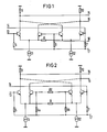
- the essentially new thing is that the collectors are combined in pairs in accordance with the phase of the collector signal and are located at two outputs, as shown by a further development of the invention shown in FIGS. 1 and 2.
- the gain control can be carried out either by current distribution control (Fig. 1) or by negative feedback control (Fig. 2).
- FIGS. 1 and 2 The invention will now be described in more detail with reference to FIGS. 1 and 2:
- a DC voltage potential V EE or the one pole of a constant current source 11 or 12 is connected to the emitters of the transistor pairs 1, 2 and 3, 4 either via a series resistor.
- the other connection of the DC voltage potential V EE lie
- the remote voltage source or the other pole of the constant current source 11 or 12 is connected to the collectors of the transistors 1, 3 or 2, 4 via a load resistor 9 or 10, respectively. These are dimensioned according to the desired step gain.
- the four transistors 1, 2, 3 and 4 are of the same type, ie either npn transistors or pnp transistors.
- the emitter of transistor 1 and the emitter of transistor 2 are connected to one another and are either connected via a series resistor with the operating potential V GG corresponding to their conductivity type or, as in FIGS. 1 and 2, with one pole of a constant current source 11.
- the base of transistor 1 forms one signal input 13.
- the collector of transistor 1 is connected to signal output 15 and also via load resistor 9 to second operating potential V CC or to the other pole of constant current source 11.
- the transistor 3 has its emitter connected to the emitter of the transistor 4. Both emitters are either connected to the same potential V EE via a series resistor at which the emitters of transistors 1 and 2 are already connected. Or there is a second constant current source 12 to which the emitters of transistors 3 and 4 are connected.
- the collector of the transistor 4 is connected to the second operating potential V CC via a load resistor 10, in the second case via the load resistor 10 to the second connection of the constant current source 12. Details of the structure of constant current sources can be found, for example, in the book by Tietze-Schenk mentioned " Semiconductor circuit technology "(1978), pages 53 to 59. , The collector of transistor 4 forms the other output terminal 16 of the transistor amplifier.
- the collector of transistor 2 is with the collector of transistor 4, the collector . of transistor 1 connected to the collector of transistor 3. 1, the base of transistor 2 is located directly on the base of transistor 3. Furthermore, the emitters of transistors 1 and 2 are connected via a negative feedback resistor 8 to the emitters of transistors 3 and 4, which means that in the definition the invention mentioned common connection between the emitters of the four transistors 1 to 4 is given. Furthermore, a reference input 17 to be acted upon by a reference potential or reference signal is provided, which is connected via a resistor 5 or 6 or 7 to the base of transistor 1, or transistors 2 and 3, or transistor 4. Finally, the base of transistor 4 is at the second input terminal 14 of the amplifier.
- the so-called current distribution control is not selected, as in FIG. 1, but the so-called negative feedback control.
- the connection between the base connections of the two transistors 2 and 3 is separated by a circuit-switching circuit R v , which is given, for example, by a conventional control circuit, such as a control circuit with two diodes or a diode ring, and then the connection between the base connections of the second transistor and the third transistor, that is, transistors 2 and 3.
- the minimum gain is obtained when the internal resistance of the circuit element Ry is infinite goes and when the size of the negative feedback resistor 8 determines the gain.
- the maximum gain is given when the internal resistance of the circuit element R V approaches zero.
Abstract
Es ist Aufgabe der Erfindung, einen monolithisch integrierbaren Transistorstromverstärker auf Grundlage von emittergekoppelten Differenzstufen zu schaffen, mit dessen Hilfe eine erhöhte Steuerfähigkeit im Vergleich zu den bekannten emittergekoppelten Differenzstufen gewährleistet ist. Um dies zu leisten, wird gemäß der Erfindung ein Transistorverstärker vorgeschlagen, der als Eingang eine emittergekoppelte Differenzstufe (1, 4) aufweist, die so mit einer basisgekoppelten Differenzstufe (2, 3) zusammengeschaltet ist, daß je ein Emitter der basisgekoppelten Differenzstufe mit je einem Emitter der emittergekoppelten Differenzstufe zusammengefaßt ist. Außerdem ist je ein Kollektor der emittergekoppelten Differenzstufe (1, 4) mit je einem Kollektor der basisgekoppelten Differenzstufe (2, 3) entsprechender Phase des Kollektorsignals zusammengeschaltet.It is an object of the invention to provide a monolithically integrable transistor current amplifier based on emitter-coupled differential stages, with the aid of which increased control capability is ensured compared to the known emitter-coupled differential stages. To achieve this, according to the invention, a transistor amplifier is proposed which has an emitter-coupled differential stage (1, 4) as input, which is connected to a base-coupled differential stage (2, 3) in such a way that one emitter of the base-coupled differential stage each has one Emitter of the emitter-coupled differential stage is summarized. In addition, one collector each of the emitter-coupled differential stage (1, 4) is interconnected with one collector of the base-coupled differential stage (2, 3) corresponding phase of the collector signal.
Description
Die Erfindung bezieht sich auf einen monolithisch integrierbaren Transistorverstärker, dessen Signaleingang an die Basis eines ersten Transistors und bei dem der Emitter dieses ersten Transistors an den Emitter eines zweiten Transistors vom selben Typ gelegt ist, bei dem ferner eine Spannungsquelle, insbesondere eine Konstantstromquelle, mit ihrem einen Anschluß an die Emitter der beiden Transistoren und mit dem anderen Anschluß über je einen Lastwiderstand an die Kollektoren der beiden Transistoren angeschlossen ist und bei dem schließlich der Signalausgang mit dem Kollektor des zweiten Transistors verbunden ist.The invention relates to a monolithically integrable transistor amplifier, the signal input to the base of a first transistor and in which the emitter of this first transistor is connected to the emitter of a second transistor of the same type, in which a voltage source, in particular a constant current source, with its a connection to the emitters of the two transistors and to the other connection via a load resistor to the collectors of the two transistors and in which the signal output is finally connected to the collector of the second transistor.
Transistorverstärkerschaltungen dieser Art sind bekannt und werden als Differenzverstärker bezeichnet und verwendet. Hierzu kann zum Beispiel das Buch von U. Tietze-Ch. Schenk "Halbleiter-Schaltungstechnik" (1978), Seite 59 genannt werden.Transistor amplifier circuits of this type are known and are referred to and used as differential amplifiers. For example, the book by U. Tietze-Ch. Schenk called "semiconductor circuit technology" (1978), page 59.
Es ist Aufgabe der Erfindung, einen monolithisch integrierbaren Transistorstromverstärker anzugeben, mit dessen Hilfe im Vergleich zu den bekannten emittergekoppelten Differenzstufen zwar ein erhöhter Stromverbrauch erforderlich ist, bei dem aber andererseits eine diesem Stromverbrauch entsprechende erhöhte Aussteuerfähigkeit gewährleistet ist. So ist zum Beispiel bei doppeltem Stromaufwand auch die doppelte Aussteuerfähigkeit gegeben. Um dasselbe zu leisten, mußten die bekannten Verstärker mit aufwendigen Reegelschaltungen versehen werden, die außerdem bei monolithischer Darstellung zu erheblichen parasitären Substratströmen und außerdem zu einem so hohen Regelstrombedarf führten, der in keinem Verhältnis mehr zu der erreichten Aussteuerfähigkeit stand. Im einzelnen ist hierzu folgendes festzustellen:It is an object of the invention to provide a monolithically integrable transistor current amplifier, with the aid of which an increased current consumption is required compared to the known emitter-coupled differential stages, but which, on the other hand, ensures an increased modulation capability corresponding to this current consumption. For example, with double the power requirement, there is twice the modulation capability. In order to do the same, the known amplifiers had to be provided with complex control circuits, which, in addition in the case of monolithic display, led to considerable parasitic substrate currents and also to such a high control current requirement, which was no longer related to the modulation capability achieved. The following can be stated in detail:
Die Signalverarbeitung in integrierten Perstärkern wird bevorzugt in symmetrischer Form durchgeführt. Der lineare Bereich einer Differenzstufe liegt dabei bei ca. 2 . UT, wobei Um die Temperaturspannung ist. Sie kann durch Emitterwiderstände um den Betrag des Spannungsabfalls an diesen Widerständen erhöht werden. Für Schaltungsanwendungen zur Verstärkungsregelung kann man zum Beispiel als Dioden geschaltete Transistoren im Emitterzweig von Differenzstufen einsetzen. Damit erreicht man im Vergleich zu den normalen emittergekoppelten Differenzstufen ohne Gegenkopplung ebenfalls eine merklich erhöhte Aussteuerfähigkeit. Jedoch führt ein solches Vorgehen in einer monolithisch integrierten Halbleiterschaltung dazu, daß durch den Betrieb der soeben angegebenen Strukturen im Restspannungsbereich der komplementäre Substrattransistor aktiviert wird, was zu einem überproportionalen Regelstrombedarf beziehungsweise bei festgehaltenem Regelstrom zu Streuungen der Verstärkung führt. Da der Nutzregelstrom in den aktiven Teil der Regelschaltung gelangt, kommt es außerdem zu einer Änderung des Arbeitspunktes der Differenzstufe sowie zu einer unerwünschten Änderung der Kollektorbetriebsspannung.The signal processing in integrated amplifiers is preferably carried out in a symmetrical form. The linear range of a differential level is approx. 2. U T , where Um is the temperature voltage. It can be increased by emitter resistors by the amount of voltage drop across these resistors. For circuit applications for gain control, it is possible, for example, to use transistors connected as diodes in the emitter branch of differential stages. In this way, compared to the normal emitter-coupled differential stages without negative feedback, a noticeably increased modulation capability is also achieved. However, such a procedure in a monolithically integrated semiconductor circuit leads to the fact that the operation of the structures just specified activates the complementary substrate transistor in the residual voltage range, which leads to a disproportionate control current requirement or recorded control current leads to scattering of the gain. Since the useful control current reaches the active part of the control circuit, there is also a change in the operating point of the differential stage and an undesirable change in the collector operating voltage.
Andererseits kann man den Gegenkopplungswiderstand im Emitter der Differenzstufe durch einen Transistor, der im Restspannungsbereich betrieben wird, kurzschließen, was aber ebenfalls zu unbefriedigenden Ergebnissen führt. Schließlich kann man für die Gegenkopplung einen Diodenring einsetzen, wodurch der negative Einfluß von. Substratströmen und die unerwünschte Änderung der Kollektorbetriebsspannung, aber nicht - ebenso wie bei den anderen soeben angedeuteten Möglichkeiten - der überhöhte Aufwand an Regelstrom vermieden werden kann.On the other hand, one can short-circuit the negative feedback resistance in the emitter of the differential stage by means of a transistor which is operated in the residual voltage range, which, however, likewise leads to unsatisfactory results. Finally, a diode ring can be used for the negative feedback, whereby the negative influence of. Substrate currents and the undesired change in the collector operating voltage, but not - as with the other possibilities just indicated - the excessive control current expenditure can be avoided.
Hier soll die Erfindung eine Abhilfe bringen:The invention is intended to remedy this:
Erfindungsgemäß wird der eingangs definierte monolithisch integrierbare Transistorverstärker derart ausgestaltet, daß vier Transistoren vom gleichen Typ vorgesehen sind und von diesen vier Transistoren zwei den ersten Transistor und den zweiten Transistor bilden, daß außerdem die Basis des zweiten Transistors mit der Basis des dritten Transistors verbunden und der dritte Transistor mit dem vierten Transistor in derselben Weise wie der erste Transistor mit dem zweiten Transistor zusammengeschaltet ist, daß ferner der Kollektor des ersten Transistors mit dem Kollektor des dritten Transistors einerseits und der Kollektor des zweiten Transistors mit dem Kollektor des vierten Transistors andererseits unmittelbar verbunden ist, daß weiterhin sowohl zwischen den Basisanschlüssen der vier Transistoren eine gemeinsame Verbindung und zwischen den Emitteranschlüssen der vier Transistoren ebenfalls eine gemeinsame Verbindung gegeben ist und daß schließlich für die Beaufschlagung der Basisanschlüsse des zweiten und dritten Transistors ein über einen Referenzeingang zuzuführendes Signal beziehungsweise Potential vorgesehen ist.According to the initially defined monolithically integrable transistor amplifier is designed such that four transistors of the same type are provided and two of these four transistors form the first transistor and the second transistor, that in addition the base of the second transistor is connected to the base of the third transistor and the third transistor is connected to the fourth transistor in the same way as the first transistor is connected to the second transistor, that further the collector of the first transistor is directly connected to the collector of the third transistor on the one hand and the collector of the second transistor is connected to the collector of the fourth transistor on the other hand that continue to have a common between both the base connections of the four transistors same connection and between the emitter connections of the four transistors there is also a common connection and that a signal or potential to be supplied via a reference input is finally provided for the application of the base connections of the second and third transistors.
Damit hat man eine regelbare Schaltungsanordnung, welche bei gleicher Aussteuerfähigkeit die durch parasitäre Ströme gegebenen Nachteile der bekannten Anordnungen vermeidet. Sie reduziert außerdem den Regelstrombedarf um den Faktor der Stromverstärkung, vermeidet nachteilige Arbeitspunktverschiebung der Kollektorspannung sowie weitere Nachteile. Außerdem kann die Stufe zur Regelung immer mit der gleichen Kollektor-Emitterspannung betrieben werden.This results in a controllable circuit arrangement which, with the same modulation capability, avoids the disadvantages of the known arrangements which are caused by parasitic currents. It also reduces the control current requirement by the factor of the current gain, avoids disadvantageous shifting of the operating point of the collector voltage and other disadvantages. In addition, the control stage can always be operated with the same collector-emitter voltage.
Bei einem Transistorverstärker gemäß der Erfindung wird auf Grund der oben gegebenen Definition eine emittergekoppelte Differenzstufe, deren Gegenkopplungswiderstand R je nach Regelumfang Werte bis R = ∞aufweisen kann, so mit einer basisgekoppelten Differenzstufe zusammengeschaltet, daß je ein Emitter der basisgekoppelten Differenzstufe mit je einem Emitter der emittergekoppelten Differenzstufe verbunden ist. Das wesentlich Neue ist, daß die Kollektoren entsprechend der Phase des Kollektorsignals paarweise zusammengefaßt sind und an zwei Ausgängen liegen, wie eine aus Fig. 1 und 2 ersichtliche Weiterbildung der Erfindung zeigt. Am Basisanschluß der basisgekoppelten Differenzstufe kann die Verstärkungsregelung entweder durch Stromverteilungssteuerang (Fig. 1) oder durch Gegenkopplungssteuerung (Fig. 2) vorgenommen werden.In a transistor amplifier according to the invention, based on the definition given above, an emitter-coupled differential stage, whose negative feedback resistance R can have values of up to R = je, depending on the scope of control, is interconnected with a base-coupled differential stage such that one emitter of the base-coupled differential stage has one emitter each emitter-coupled differential stage is connected. The essentially new thing is that the collectors are combined in pairs in accordance with the phase of the collector signal and are located at two outputs, as shown by a further development of the invention shown in FIGS. 1 and 2. At the base connection of the base coupled differential stage, the gain control can be carried out either by current distribution control (Fig. 1) or by negative feedback control (Fig. 2).
Die Erfindung wird nun an Hand der Fig. 1 und 2 näher beschrieben:The invention will now be described in more detail with reference to FIGS. 1 and 2:
Zwischen den beiden Eingangsanschlüssen 13., 14 liegt das symmetrische Eingangssignal. Die Transistoren und 4 sind die Eingangstransistoren, deren Emitterverkopplung durch den Gegenkopplungswiderstand 8 festgelegt wird. Transistor 2 und Transistor 3 stellen eine basisgekoppelte Differenzstufe dar, die durch eine Steuerleitung 18 bei der in Fig. 1 ersichtlichen Ausgestaltung in ihrem Arbeitspunkt und somit in der Verstärkung eingestellt werden kann. Maximale Verstärkung erhält man dann, wenn der Strom durch alle vier Transistoren 1, 2, 3 und 4 gleiche Beträge aufweist und der Gegenkopplungswiderstand 8 durch die symmetrisch wirksame Emittereingangsimpedanz von Transistor 3 und Transistor 4 auf den Wert
- UT = Temperaturspannung
- IE3,4 = Emitterstrom
- rb = Basisbahnwiderstand
- ß = Wechselstromverstärkung in Emitterschaltung
ist.The symmetrical input signal lies between the two
- U T = temperature voltage
- IE 3.4 = emitter current
- r b = baseline resistance
- ß = alternating current gain in emitter circuit
is.
An die Emitter der Transistorpaare 1, 2 und 3, 4 ist entweder über je einen Vorwiderstand ein Gleichspannungspotential VEE oder der eine Pol einer Konstantstromquelle 11 beziehungsweise 12 angeschlossen. Der andere Anschluß der das Gleichspannungspotential VEE liefernden Spannungsquelle beziehungsweise der andere Pol der Konstantstromquelle 11 beziehungsweise 12 liegt über je einen Lastwiderstand 9 beziehungsweise 10 an den Kollektoren der Transistoren 1, 3 beziehungsweise 2, 4. Diese werden entsprechend der gewünschten Stufenverstärkung bemessen.A DC voltage potential V EE or the one pole of a constant current source 11 or 12 is connected to the emitters of the
Entsprechend der oben gegebenen Definition der Erfindung sind die vier Transistoren 1, 2, 3 und 4 vom selben Typ, also entweder npn-Transistoren oder pnp-Transistoren. Der Emitter des Transistors 1 und der Emitter des Transistors 2 sind miteinander verbunden und werden entweder über einen Vorwiderstand mit dem ihrem Leitungstyp entsprechenden Betriebspotential VGG oder, wie in Fig. 1 und 2, mit dem einen Pol einer Konstantstromquelle 11 verbunden. Die Basis des Transistors 1 bildet den einen Signaleingang 13. Der Kollektor des Transistors 1 liegt am Signalausgang 15 und außerdem über den Lastwiderstand 9 am zweiten Betriebspotential VCC oder am anderen Pol der Konstantstromquelle 11.According to the definition of the invention given above, the four
Der Transistor 3 ist mit seinem Emitter mit dem Emitter des Transistors 4 verbunden. Beide Emitter werden entweder über einen Vorwiderstand an dasselbe Potential VEE gelegt, an welchem bereits die Emitter der Transistoren 1 und 2 angeschaltet sind. Oder es ist eine zweite Konstantstromquelle 12 vorgesehen, an derem einen Anschluß die Emitter der Transistoren 3 und 4 liegen. Im erstgenannten Fall liegt der Kollektor des Transistors 4 über einen Lastwiderstand 10 am zweiten Betriebspotential VCC, im zweiten Fall über den Lastwiderstand 10 am zweiten Anschluß der Konstantstromquelle 12. Einzelheiten über den Aufbau von Konstantstromquellen sind zum Beispiel dem genannten Buch von Tietze-Schenk "Halbleiter-Schaltungstechnik" (1978), Seiten 53 bis 59 zu entnehmen. , Der Kollektor des Transistors 4 bildet die andere Ausgangsklemme 16 des-Transistorverstärkers. Der Kollektor des Transistors 2 ist mit dem Kollektor des Transistors 4, der Kollektor.des Transistors 1 mit dem Kollektor des Transistors 3 verbunden. Ferner liegt bei der Ausgestaltung gemäß Fig. 1 die Basis des Transistors 2 unmittelbar an der Basis des Transistors 3. Ferner sind die Emitter der Transistoren 1 und 2 über einen Gegenkopplungswiderstand 8 mit den Emittern der Transistoren 3 und 4 verbunden, wodurch die in der Definition der Erfindung erwähnte gemeinsame Verbindung zwischen den Emittern der vier Transistoren 1 bis 4 gegeben ist. Ferner ist ein durch ein Referenzpotential beziehungsweise Referenzsignal zu beaufschlagender Referenzeingang 17 vorgesehen, der über je einen Widerstand 5 beziehungsweise 6, beziehungsweise 7 mit der Basis des Transistors 1, beziehungsweise der Transistoren 2 und 3, beziehungsweise des Transistors 4 verbunden ist. Schließlich liegt die Basis des Transistors 4 an der zweiten Eingangsklemme 14 des Verstärkers.The
In der Schaltungsanordnung gemäß Fig. 2 ist nicht, wie bei Fig. 1, die sogenannte Stromverteilungsregelung, sondern die sogenannte Gegenkopplungsregelung gewählt. Hier ist die Verbindung zwischen den Basisanschlüssen der beiden Transistoren 2 und 3 durch ein die Regelung vermittelndes Schaltungsglied Rv aufgetrennt, das zum Beispiel durch eine übliche Regelschaltung, wie zum Beispiel eine Regelschaltung mit zwei Dioden oder einem Diodenring, gegeben ist und dann die Verbindung zwischen den Basisanschlüssen des zweiten Transistors und des dritten Transistors, also der Transistoren 2 und 3, bildet. Die minimale Verstärkung erhält man dann, wenn der Innenwiderstand des Schaltungsglieds Ry gegen unendlich geht und wenn die Größe des Gegenkopplungswiderstands 8 die Verstärkung festlegt. Die maximale Verstärkung ist dann gegeben, wenn der Innenwiderstand des Schaltungsglieds RV gegen Null geht.In the circuit arrangement according to FIG. 2, the so-called current distribution control is not selected, as in FIG. 1, but the so-called negative feedback control. Here, the connection between the base connections of the two
Claims (5)
Applications Claiming Priority (2)
| Application Number | Priority Date | Filing Date | Title |
|---|---|---|---|
| DE2924171 | 1979-06-15 | ||
| DE19792924171 DE2924171A1 (en) | 1979-06-15 | 1979-06-15 | MONOLITHICALLY INTEGRATED TRANSISTOR AMPLIFIER |
Publications (3)
| Publication Number | Publication Date |
|---|---|
| EP0021085A2 true EP0021085A2 (en) | 1981-01-07 |
| EP0021085A3 EP0021085A3 (en) | 1981-03-18 |
| EP0021085B1 EP0021085B1 (en) | 1984-04-11 |
Family
ID=6073269
Family Applications (1)
| Application Number | Title | Priority Date | Filing Date |
|---|---|---|---|
| EP80102972A Expired EP0021085B1 (en) | 1979-06-15 | 1980-05-28 | Monolithically integratable transistor amplifier |
Country Status (4)
| Country | Link |
|---|---|
| US (1) | US4369410A (en) |
| EP (1) | EP0021085B1 (en) |
| JP (1) | JPS564908A (en) |
| DE (1) | DE2924171A1 (en) |
Cited By (1)
| Publication number | Priority date | Publication date | Assignee | Title |
|---|---|---|---|---|
| EP0397250A2 (en) * | 1989-05-10 | 1990-11-14 | Philips Electronics Uk Limited | D.C. blocking amplifier |
Families Citing this family (8)
| Publication number | Priority date | Publication date | Assignee | Title |
|---|---|---|---|---|
| US4621831A (en) * | 1984-09-06 | 1986-11-11 | Nhk Spring Co., Ltd. | Stabilizer for motor vehicle |
| JPS6173156A (en) * | 1984-09-19 | 1986-04-15 | Toray Ind Inc | Water-free lithographic plate |
| JPH0682213B2 (en) * | 1986-06-16 | 1994-10-19 | 東レ株式会社 | Waterless planographic printing plate |
| EP0600141B1 (en) * | 1992-10-30 | 1997-03-05 | SGS-THOMSON MICROELECTRONICS S.p.A. | Transconductor stage |
| JPH07110574A (en) * | 1993-12-13 | 1995-04-25 | Toray Ind Inc | Production of waterless lithographic printing plate |
| JPH08102629A (en) * | 1994-09-30 | 1996-04-16 | Ando Electric Co Ltd | Differential amplifier circuit |
| GB9906026D0 (en) | 1999-03-16 | 1999-05-12 | Mitel Semiconductor Ltd | An amplifier circuit arrangement |
| KR100485796B1 (en) * | 2003-01-23 | 2005-04-28 | 삼성전자주식회사 | Boosting circuit |
Citations (2)
| Publication number | Priority date | Publication date | Assignee | Title |
|---|---|---|---|---|
| US3843934A (en) * | 1973-01-31 | 1974-10-22 | Advanced Micro Devices Inc | High speed transistor difference amplifier |
| US4146844A (en) * | 1977-10-31 | 1979-03-27 | Tektronix, Inc. | Feed-forward amplifier |
Family Cites Families (9)
| Publication number | Priority date | Publication date | Assignee | Title |
|---|---|---|---|---|
| GB915404A (en) * | 1961-01-13 | 1963-01-09 | Marconi Wireless Telegraph Co | Improvements in or relating to variable gain circuit arrangements |
| US3452289A (en) * | 1967-02-16 | 1969-06-24 | Motorola Inc | Differential amplifier circuits |
| NL162802C (en) * | 1971-10-09 | 1980-06-16 | Philips Nv | INTEGRATED DIFFERENCE AMPLIFIER. |
| DE2230431C3 (en) * | 1972-06-22 | 1982-12-16 | Robert Bosch Gmbh, 7000 Stuttgart | Circuit arrangement for the symmetrical control of a differential amplifier |
| JPS49104549A (en) * | 1973-02-07 | 1974-10-03 | ||
| US3846712A (en) * | 1973-03-12 | 1974-11-05 | Bell Telephone Labor Inc | Differential amplifier with dynamic biasing |
| JPS5921233B2 (en) * | 1976-09-14 | 1984-05-18 | ソニー株式会社 | stereo demodulation circuit |
| US4109214A (en) * | 1977-05-31 | 1978-08-22 | Motorola, Inc. | Unbalanced-to-balanced signal converter circuit |
| JPS6045166B2 (en) * | 1977-06-24 | 1985-10-08 | 株式会社クラレ | Method for producing 3-(β-hydroxyethyl)butenols |
-
1979
- 1979-06-15 DE DE19792924171 patent/DE2924171A1/en active Granted
-
1980
- 1980-05-28 EP EP80102972A patent/EP0021085B1/en not_active Expired
- 1980-06-05 US US06/156,863 patent/US4369410A/en not_active Expired - Lifetime
- 1980-06-12 JP JP7960080A patent/JPS564908A/en active Pending
Patent Citations (2)
| Publication number | Priority date | Publication date | Assignee | Title |
|---|---|---|---|---|
| US3843934A (en) * | 1973-01-31 | 1974-10-22 | Advanced Micro Devices Inc | High speed transistor difference amplifier |
| US4146844A (en) * | 1977-10-31 | 1979-03-27 | Tektronix, Inc. | Feed-forward amplifier |
Non-Patent Citations (1)
| Title |
|---|
| IEEE JOURNAL OF SOLID STATE CIRCUITS, Band SC-3, Nr. 4, Dezember 1968, New York US, B. GILBERT: "A new wide-band amplifier technique", Seiten 353-365. * |
Cited By (2)
| Publication number | Priority date | Publication date | Assignee | Title |
|---|---|---|---|---|
| EP0397250A2 (en) * | 1989-05-10 | 1990-11-14 | Philips Electronics Uk Limited | D.C. blocking amplifier |
| EP0397250A3 (en) * | 1989-05-10 | 1991-10-02 | Philips Electronics Uk Limited | D.c. blocking amplifier |
Also Published As
| Publication number | Publication date |
|---|---|
| DE2924171C2 (en) | 1987-12-17 |
| EP0021085A3 (en) | 1981-03-18 |
| JPS564908A (en) | 1981-01-19 |
| EP0021085B1 (en) | 1984-04-11 |
| US4369410A (en) | 1983-01-18 |
| DE2924171A1 (en) | 1980-12-18 |
Similar Documents
| Publication | Publication Date | Title |
|---|---|---|
| DE3103969C2 (en) | "Supply voltage driver for a differential amplifier" | |
| DE3114877C2 (en) | Current mirror circuit | |
| DE3012965C2 (en) | ||
| DE1901804B2 (en) | STABILIZED DIFFERENTIAL AMPLIFIER | |
| DE2837853C3 (en) | Differential amplifier | |
| DE2207233C3 (en) | Electronic signal amplifier | |
| DE3937501A1 (en) | METHOD AND DEVICE FOR GENERATING A PRELOAD | |
| DE4113498C1 (en) | ||
| DE2648577A1 (en) | ELECTRICALLY CHANGEABLE IMPEDANCE CIRCUIT | |
| DE2416534A1 (en) | COMPLEMENTARY-SYMMETRIC AMPLIFIER CIRCUIT | |
| EP0021085B1 (en) | Monolithically integratable transistor amplifier | |
| DE69725277T2 (en) | Low noise amplifier | |
| DE2443137C2 (en) | Differential amplifier | |
| DE2905659A1 (en) | PACKAGING AMPLIFIER CIRCUIT | |
| DE3545392C2 (en) | ||
| DE2409929C3 (en) | Low-distortion, low-frequency push-pull power amplifier | |
| EP0237086B1 (en) | Current mirror circuit | |
| DE3210661A1 (en) | AMPLIFIER | |
| DE3810058A1 (en) | SCHMITT TRIGGER CIRCUIT | |
| DE2946952C2 (en) | ||
| DE60133068T2 (en) | DIFFERENTIALLY ARRANGED TRANSISTOR PAIR WITH MEDIUM FOR THE DEGENERATION OF TRANSCONDUCTANCE | |
| DE3243706C1 (en) | ECL-TTL signal level converter | |
| DE3229437C2 (en) | ||
| DE2148880C2 (en) | Power source in integrated circuit technology | |
| DE3145771C2 (en) |
Legal Events
| Date | Code | Title | Description |
|---|---|---|---|
| PUAI | Public reference made under article 153(3) epc to a published international application that has entered the european phase |
Free format text: ORIGINAL CODE: 0009012 |
|
| AK | Designated contracting states |
Designated state(s): FR GB IT |
|
| PUAL | Search report despatched |
Free format text: ORIGINAL CODE: 0009013 |
|
| AK | Designated contracting states |
Designated state(s): FR GB IT |
|
| 17P | Request for examination filed |
Effective date: 19810626 |
|
| ITF | It: translation for a ep patent filed |
Owner name: STUDIO JAUMANN |
|
| GRAA | (expected) grant |
Free format text: ORIGINAL CODE: 0009210 |
|
| AK | Designated contracting states |
Designated state(s): FR GB IT |
|
| ET | Fr: translation filed | ||
| PLBE | No opposition filed within time limit |
Free format text: ORIGINAL CODE: 0009261 |
|
| STAA | Information on the status of an ep patent application or granted ep patent |
Free format text: STATUS: NO OPPOSITION FILED WITHIN TIME LIMIT |
|
| 26N | No opposition filed | ||
| PGFP | Annual fee paid to national office [announced via postgrant information from national office to epo] |
Ref country code: GB Payment date: 19890430 Year of fee payment: 10 |
|
| PGFP | Annual fee paid to national office [announced via postgrant information from national office to epo] |
Ref country code: FR Payment date: 19890522 Year of fee payment: 10 |
|
| ITTA | It: last paid annual fee | ||
| PG25 | Lapsed in a contracting state [announced via postgrant information from national office to epo] |
Ref country code: GB Effective date: 19900528 |
|
| GBPC | Gb: european patent ceased through non-payment of renewal fee | ||
| PG25 | Lapsed in a contracting state [announced via postgrant information from national office to epo] |
Ref country code: FR Effective date: 19910131 |
|
| REG | Reference to a national code |
Ref country code: FR Ref legal event code: ST |