EP0903927B1 - Circuit de transistors MOS avec fonction transformateur/interface de données - Google Patents
Circuit de transistors MOS avec fonction transformateur/interface de données Download PDFInfo
- Publication number
- EP0903927B1 EP0903927B1 EP97830462A EP97830462A EP0903927B1 EP 0903927 B1 EP0903927 B1 EP 0903927B1 EP 97830462 A EP97830462 A EP 97830462A EP 97830462 A EP97830462 A EP 97830462A EP 0903927 B1 EP0903927 B1 EP 0903927B1
- Authority
- EP
- European Patent Office
- Prior art keywords
- substitutive
- voltage
- mos transistors
- transistors
- supply
- Prior art date
- Legal status (The legal status is an assumption and is not a legal conclusion. Google has not performed a legal analysis and makes no representation as to the accuracy of the status listed.)
- Expired - Lifetime
Links
Images


Classifications
-
- H—ELECTRICITY
- H04—ELECTRIC COMMUNICATION TECHNIQUE
- H04Q—SELECTING
- H04Q11/00—Selecting arrangements for multiplex systems
- H04Q11/04—Selecting arrangements for multiplex systems for time-division multiplexing
- H04Q11/0428—Integrated services digital network, i.e. systems for transmission of different types of digitised signals, e.g. speech, data, telecentral, television signals
- H04Q11/0435—Details
-
- H—ELECTRICITY
- H04—ELECTRIC COMMUNICATION TECHNIQUE
- H04L—TRANSMISSION OF DIGITAL INFORMATION, e.g. TELEGRAPHIC COMMUNICATION
- H04L12/00—Data switching networks
-
- H—ELECTRICITY
- H04—ELECTRIC COMMUNICATION TECHNIQUE
- H04M—TELEPHONIC COMMUNICATION
- H04M19/00—Current supply arrangements for telephone systems
- H04M19/08—Current supply arrangements for telephone systems with current supply sources at the substations
-
- H—ELECTRICITY
- H04—ELECTRIC COMMUNICATION TECHNIQUE
- H04Q—SELECTING
- H04Q2213/00—Indexing scheme relating to selecting arrangements in general and for multiplex systems
- H04Q2213/13003—Constructional details of switching devices
-
- H—ELECTRICITY
- H04—ELECTRIC COMMUNICATION TECHNIQUE
- H04Q—SELECTING
- H04Q2213/00—Indexing scheme relating to selecting arrangements in general and for multiplex systems
- H04Q2213/1308—Power supply
-
- H—ELECTRICITY
- H04—ELECTRIC COMMUNICATION TECHNIQUE
- H04Q—SELECTING
- H04Q2213/00—Indexing scheme relating to selecting arrangements in general and for multiplex systems
- H04Q2213/13082—Power supply via phantom line
-
- H—ELECTRICITY
- H04—ELECTRIC COMMUNICATION TECHNIQUE
- H04Q—SELECTING
- H04Q2213/00—Indexing scheme relating to selecting arrangements in general and for multiplex systems
- H04Q2213/1309—Apparatus individually associated with a subscriber line, line circuits
-
- H—ELECTRICITY
- H04—ELECTRIC COMMUNICATION TECHNIQUE
- H04Q—SELECTING
- H04Q2213/00—Indexing scheme relating to selecting arrangements in general and for multiplex systems
- H04Q2213/13166—Fault prevention
-
- H—ELECTRICITY
- H04—ELECTRIC COMMUNICATION TECHNIQUE
- H04Q—SELECTING
- H04Q2213/00—Indexing scheme relating to selecting arrangements in general and for multiplex systems
- H04Q2213/13202—Network termination [NT]
-
- H—ELECTRICITY
- H04—ELECTRIC COMMUNICATION TECHNIQUE
- H04Q—SELECTING
- H04Q2213/00—Indexing scheme relating to selecting arrangements in general and for multiplex systems
- H04Q2213/13209—ISDN
-
- H—ELECTRICITY
- H04—ELECTRIC COMMUNICATION TECHNIQUE
- H04Q—SELECTING
- H04Q2213/00—Indexing scheme relating to selecting arrangements in general and for multiplex systems
- H04Q2213/13305—Transistors, semiconductors in general
-
- H—ELECTRICITY
- H04—ELECTRIC COMMUNICATION TECHNIQUE
- H04Q—SELECTING
- H04Q2213/00—Indexing scheme relating to selecting arrangements in general and for multiplex systems
- H04Q2213/1332—Logic circuits
-
- H—ELECTRICITY
- H04—ELECTRIC COMMUNICATION TECHNIQUE
- H04Q—SELECTING
- H04Q2213/00—Indexing scheme relating to selecting arrangements in general and for multiplex systems
- H04Q2213/13322—Integrated circuits
-
- Y—GENERAL TAGGING OF NEW TECHNOLOGICAL DEVELOPMENTS; GENERAL TAGGING OF CROSS-SECTIONAL TECHNOLOGIES SPANNING OVER SEVERAL SECTIONS OF THE IPC; TECHNICAL SUBJECTS COVERED BY FORMER USPC CROSS-REFERENCE ART COLLECTIONS [XRACs] AND DIGESTS
- Y02—TECHNOLOGIES OR APPLICATIONS FOR MITIGATION OR ADAPTATION AGAINST CLIMATE CHANGE
- Y02D—CLIMATE CHANGE MITIGATION TECHNOLOGIES IN INFORMATION AND COMMUNICATION TECHNOLOGIES [ICT], I.E. INFORMATION AND COMMUNICATION TECHNOLOGIES AIMING AT THE REDUCTION OF THEIR OWN ENERGY USE
- Y02D30/00—Reducing energy consumption in communication networks
- Y02D30/70—Reducing energy consumption in communication networks in wireless communication networks
Definitions
- This invention relates to a MOS transistors substitutive circuit having a transformer/data interface function, particularly for ISDN networks, and corresponding control and driving switch configuration.
- the invention relates to a MOS transistors substitutive circuit having a transformer/data interface function, particularly for ISDN networks, which circuit comprises first and second power supply/transmitter blocks, said first power supply/transmitter block being connected between a voltage reference and a first data interface, and said second power supply/transmitter block being connected between a ground potential reference and a second data interface, said first and second power supply/transmitter blocks being further connected to a supply voltage reference.
- the invention also relates to a control and driving switch configuration for substitutive transformer/data transmitter circuits in a network termination, in particular ISDN network terminations, said network termination including first and second converters connected to a ground potential reference, said first converter delivering a supply voltage and an emergency voltage and said second converter delivering a remote supply voltage.
- the invention particularly, but not exclusively, concerns an ISDN network termination, and the description that follows will make reference to that application for simplicity of illustration.
- An important additional function is, besides voice transmission, the transmission of information relating to new products and/or services, such as facsimile operations, video communications, network interconnections, etc..
- the transmission of data by a telephone terminal unit may utilize special networks.
- One example of a well known and widely utilized network is the ISDN (Integrated Services Digital Network), originating by natural evolution from the traditional telephone network and employing the same standard cables. This compatibility of transmission with the traditional telephone network allows the ISDN network to use the so-called telephone loops, which are advantageously available throughout the territory.
- ISDN Integrated Services Digital Network
- the ISDN network is to European standard, having a transmit rate of 64 kbit/sec; the ISDN network allows two talk channels plus a control and service channel to be sent over the same line, which channels can be either used by two telephone sets, or one telephone set and a facsimile, or one telephone set and a PC (Personal Computer).
- Figure 1 Shown by way of example in Figure 1 is a block diagram for basic access to the ISDN network. This diagram is also shown in Figure 2, in greater detail.
- FIG. 1 Also shown in Figure 1 are first U, second S and third R reference points, whereat special interface circuits are connected, as detailed in Figure 2 for the references U and S only.
- the line termination LT provides for power supply in the remote mode to the network termination NT, and in an emergency condition known in the art as RM (Restricted Mode), for a terminal apparatus TE as well.
- RM Remote Mode
- the line termination LT allows signal data DS to be transmitted and received in suitable formats, such as the 2B1Q or 4B3T formats, through the interface circuits of the reference point U.
- the terminal adapter TA connected in the reference point R, allows apparatus designed for different data transmission modes, usually commercially available apparatus, to be also connected to the network termination NT.
- the network termination NT is connected to the line termination LT by a two-wire telephone loop, whereby the network termination NT can be powered from the line termination LT and can exchange with it data DS simultaneously in either directions.
- the network termination NT is provided with a DC/DC converter CONV1 capable of delivering a supply voltage VDD, typically of 5V, to the interface circuits at the reference points U and S, as well as an emergency voltage Vem.
- VDD supply voltage
- Vem emergency voltage
- the emergency voltage Vem of about 40V, can only be used in an RM emergency condition to power the terminal apparatus TE, with some suitable constraints.
- Such terminal apparatus TE are normally powered from an AC/DC converter CONV2 provided at the network termination NT and capable of powering up to eight terminal apparatuses TE, according to the standard applied.
- the emergency voltage Vem is disconnected by means of a first switch arrangement SW, shown in Figure 2, which is closed at the AC/DC converter CONV2.
- the network termination NT has two input terminals A, B and four output terminals A', A'' and B', B'', two for each transformer of the interface circuit at the reference point S, as previously shown schematically in Figure 1.
- the output terminals A', A'' and B', B'' provide for remote power supply and data transmission through a supply/data transmission block BT comprising a DC/DC converter CONV3, a transmit block TX', and a receive block RX', so as to communicate with the terminal apparatus TE.
- the transmit and receive blocks, TX', RX' are schematically represented in Figure 2 by simple transformers serving to receive the power supply and allow of the data, present in the transmit and receive blocks TX', RX', conversion.
- power to the terminal apparatus TE is supplied from the interface circuits at the reference point S by means of the transformers, shown schematically in Figure 2, which are also utilized for exchanging the signal data DS.
- These transformers allow a virtually zero DC voltage drop to be obtained, and have an AC impedance which is a function of load and the winding ratio of the transformer.
- the supply to the terminal apparatus TE under RM emergency conditions is controlled through the switches SW.
- the combination of the transformers in the interface circuits at the reference point S and the switches SW controlling the supply to the terminal apparatus TE form a transformer/data interface/switch circuit for effecting a polarity reversal CT according to the prior art.
- transformers for powering or effecting the exchange of signal data DS at the interface circuits, is specially convenient from the standpoint of energy dissipation. Minimizing energy dissipation is highly important under RM emergency conditions; in such circumstances, in fact, no mains supply would be available, and the available power would be limited to the small power that the DC/DC converter at the interface circuits of the reference point U can draw on the line.
- transformers must be designed to meet specific applicational requirements, thereby producing a manufacturing cost.
- circuits including active components are described in US Patents No. 3,649,769 to Pest, No. 4,004,104 to Picandet et al., No. 3,943,432 to Colardelle et al., and No. 4,088,843 to Rogers et al..
- the prior art active component circuits are less expensive than transformers. But they are unsatisfactory from the energy dissipation standpoint, and still require suitable switches for supply control.
- the underlying technical problem of this invention is to provide a transformer/data interface circuit emulating a transformer for an ISDN telephone line, which can transmit the data presented on the line, transmit and control the power supply to the terminal apparatus (reversal of current polarity or direction), and has suitable structural and functional features to afford reduced energy consumption and overcome the drawbacks that are still besetting the prior art devices.
- circuits comprising MOS transistors which operate in the saturation range, and are suitably configured as diodes through common resistors, substitutes the transformer/data interface/switch circuit comprising the combined transformers and power supply control switches as provided at the network termination in the prior art, so as to present a high A.C. impedance and virtually zero D.C. impedance, thus minimizing the overall dissipation of power by the network termination, and allowing the power supply to be controlled under any conditions of operation of the network termination, while effecting the reversal in the current direction.
- control and driving switch configuration for substitutive transformer/data transmitter circuits in a network termination, as previously indicated and defined in the characterizing part of Claim 23.
- the control configuration selects the voltage reference to be applied to the power supply/transmitter blocks.
- FIG. 1 generally and schematically shown at 1 is a network termination according to the invention, wherein the transmission of data is not illustrated.
- Figure 3 illustrates in particular a power supply distribution through the network termination 1, comprising first 2 and second 3 converters, specifically a DC/DC converter and an AC/DC converter.
- the architecture of the network termination 1 of Figure 3 may also be used for data transmission.
- the first DC/DC converter 2 is connected to a ground potential reference GND, and delivers a supply voltage VDD, e.g. of either 5V or 3.3V, and an emergency voltage Vem, typically of 40V, similar to the DC/DC converter CONV1 described above in connection with the prior art.
- the second AC/DC converter 3 is connected to the ground potential reference GND and issues a polarity reversal control signal Scrp and a remote supply voltage VR, typically of 48V, on a signal line BUS1.
- the first 2 and second 3 converters are also connected to a first RM emergency condition supply block 4 and a second normal condition supply block 5, respectively, comprising P-channel MOS or PMOS transistors.
- a current limiter 6 which is set, for example, to a value in the 9mA to 11mA range, harmonizing with regulations.
- the first 4 and second 5 supply blocks are connected to a third normal condition supply block 7 and a fourth RM emergency condition supply block 8, respectively, which comprise N-channel MOS or NMOS transistors.
- the third 7 and fourth 8 supply blocks are also connected to the ground potential reference GND.
- first 4 and fourth 8 supply blocks are connected directly to the signal line BUS1, while the second 5 and third 7 supply blocks are connected thereto through first 9 and second 10 logic inverters.
- the second 5 and fourth 8 supply blocks are connected to a first data interface RX, and the first 4 and third 7 supply blocks are connected to a second data interface TX.
- the block RL schematically shown in Figure 3 as being connected to the data interfaces RX and TX, represents an equivalent DC resistor of a power supply/data transmission receive block connected to these interfaces and needed by the terminal apparatus TE.
- the network termination 1 comprises first 11 and second 11' MOS transistors substitutive circuits having a transformer/data interface function, respectively comprising normal condition supply blocks 5, 7 and RM emergency condition supply blocks 4, 8.
- the emergency voltage Vem and remote supply voltage VR are respectively applied to the supply blocks 5, 7 and 4, 8 in a first condition of operation, referred to as the normal operation condition, and in a second condition of operation, referred to as the emergency condition, of the network termination 1.
- a MOS transistors substitutive circuit having a transformer/data interface function, according to the invention, is shown best in Figure 4.
- the substitutive circuit 11 comprises first 11a and second 11b power supply/transmitter blocks, which essentially correspond to the first supply block 4 in the RM emergency condition, or to the second supply block 5 in the normal condition, and to the fourth supply block 8 in the RM emergency condition, or the third supply block 7 in the normal condition, respectively.
- This substitutive circuit 11 is implemented by a first pair 12 of P-channel MOS or PMOS transistors, and a second pair 12' of N-channel MOS or NMOS transistors.
- the transistors of each pair 12, 12' draw the same DC current in the connection leads to the first RX and second TX data interfaces.
- first 12 and second 12' MOS transistor pairs are easily constructed from basic components made available by conventional mixed technologies of the BCD type.
- FIG. 4 shows that either (respectively PMOS and NMOS) transistor pairs 12, 12' are diode connected through suitable connection resistors.
- the first transistor pair 12 of the first power supply/transmitter block 11a comprises first M1 and second M2 P-channel transistors which are connected to a voltage reference V corresponding either to the remote supply voltage VR or the emergency voltage Vem, according to the operation condition of the network termination whereto the substitutive transformer/data interface circuit 11 is incorporated.
- the first M1 and second M2 transistors are also connected to the first data interface RX, and have their gate terminals in common and connected to the respective drain terminals through first R1 and second R2 connection resistors.
- the drain terminals of the transistors M1 and M2 are connected to the first data interface RX through a suitable decoupling circuit 13 which comprises at least one cross-connection resistor 14 and suitable common mode inductors.
- the drain terminals of the transistors M1 and M2 are also connected to a voltage/current converter 15 through first C1 and second C2 decoupling capacitors, respectively, which capacitors are further connected to a reference voltage reference VREF through first R3 and second R4 bias resistors.
- the voltage/current converter 15 is connected between the supply voltage reference VDD and the ground potential reference GND, and further connected to the supply voltage reference VDD via first 16 and second 17 current mirrors.
- the first 16 and second 17 current mirrors are connected to first 18 and second 19 amplifier circuits which are connected between the supply voltage reference VDD and the ground potential reference GND and connected, in parallel with each other, to a control terminal OUT whereat a voltage value equal to one half the supply voltage VDD is present.
- an output voltage which is proportional to the voltage present on the line, limited to the conditions of the signal AC; this output voltage can be modulated by means of the current mirrors 16 and 17 and the resistors included in the amplifier circuits 18 and 19.
- the second transistor pair 12' of the second power supply/transmitter block 11b comprises first M1' and second M2' N-channel transistors being connected between the ground potential reference GND and the second data interface TX and having their gate terminals in common and connected to the respective drain terminals through first R1' and second R2' connection resistors.
- the first M1' and second M2' transistors have their source terminals in common and connected, through a suitable sensing resistor Rgnd (unessential to the aim of the invention), to the ground potential reference GND, and have their drain terminals connected to first D1 and second D2 decoupling elements, e.g. two diodes, and connected to the second data interface TX via a suitable decoupling circuit 13' which comprises at least one cross-connection resistor 14' and suitable common mode inductors.
- drain terminals of the transistors M1' and M2' are also connected, through the decoupling elements D1 and D2, to first 16' and second 17' current mirrors which are further connected to the supply voltage reference VDD and decoupled from the second data interface TX by means of first C1' and second C2' decoupling capacitors.
- the decoupling elements D1 and D2 operate in particular supply conditions of the substitutive circuit 11.
- the first C1' and second C2' decoupling capacitors are also connected to the ground potential reference GND through third 20 and fourth 21 current mirrors.
- the first 16' and second 17' current mirrors are connected to both the third 20 and fourth 21 current mirrors in crossed manner, thereby forming a "bridge" connection.
- the first 16' and second 17' current mirrors are also connected to a buffer circuit 22 through first R5 and second R6 decoupling resistors, respectively, and connected to a voltage/current converter 15' which has first C and second D input terminals.
- the buffer 22 is connected between the supply voltage reference VDD and the ground potential reference GND, and connected to the reference voltage reference VREF.
- the buffer 22 sets the output reference voltage VREF for the current mirrors 16', 17', 20 and 21.
- the decoupling resistors R5 and R6 will then establish an impedance between the current mirrors 17', 21 and 16', 20, respectively, suitable to provide, in a condition of AC current, a higher impedance value than the resistance value of the cross-connection 14' in the decoupling circuit 13'.
- the buffer 22 thus will, in cooperation with the decoupling resistors R5 and R6, set the working voltage of the current mirrors without altering the line impedance value across the cross-connection resistor 14'.
- the reference voltage VREF is one half the supply voltage VDD.
- a differential data signal specifically a voltage, presented across the cross-connection resistor 14 of the decoupling circuit 13 associated with the first data interface RX, will "see” a high impedance through the transistors M1 and M2, and especially through the parallel connection of the resistors R1, R2, R3 and R4.
- This differential data signal then travels through the decoupling capacitors C1 and C2 to the voltage/current converter 15, where it is converted to a current.
- the differential current data signal then goes through the current mirrors 16 and 17 to be ultimately converted back to a voltage by the amplifier circuits 18 and 19.
- the differential data signal associated with the first data interface RX will again be presented, suitably amplified, at the output terminals A and B of the amplifier circuits 18 and 19.
- the final amplification value of the differential data signal can be programmed by varying the ratio of the current mirrors 16, 17 and the resistance values used.
- a differential data signal such as a voltage
- a differential data signal at the input terminals C and D of the voltage/current converter 15' in the second power supply/transmitter block 11b is converted to a current and transmitted to the bridge configuration of the current mirrors 16', 17', 20 and 21.
- the differential data signal converted to a current has a first polarity, it is input, through the decoupling capacitor C1' connected to the first current mirror 16', to a first terminal of the cross-connection resistor 14' of the decoupling circuit 13' associated with the second data interface TX, to then loop back to ground through the decoupling capacitor C2' and the fourth current mirror 21.
- the second power supply/transmitter block 11b can be said to replicate, at the second data interface TX, the differential data signal presented to the input of the voltage/current converter 15'.
- This differential data signal is output with said first polarity.
- the differential current data signal has a second polarity, in particular a reversed polarity form the first, it is input, through the decoupling capacitor C2' connected to the second current mirror 17', to a second terminal of the cross-connection resistor 14' of the decoupling circuit 13' associated with the second data interface TX, to then loop back to ground through the decoupling capacitor C1' and the third current mirror 20.
- connection to the cross-connection resistor 14' is the reverse from the previously discussed differential data signal having a first polarity, and the second power supply/transmitter block 11b will replicate the differential data signal, presented to the input of the voltage/current converter 15' and having said second polarity, at the second data interface TX.
- the transistors M1 and M2 would offer, in fact, a low resistance to the passage of said supply current.
- the mid-point terminal of the interface transformers in the first data interface RX is suitably connected to the mid-point terminal of the interface transformers in the second data interface TX, thereby allowing the supply current to cross the decoupling circuit 13'.
- the equivalent resistance of this connection is schematically represented by the block RL in Figure 4.
- the supply current path then loops back to ground through the transistors M1' and M2'.
- MOS transistors substitutive circuit of the invention replaces, therefore, the transformers associated with the interface at the reference point S in the prior art.
- the polarity reversal control signal Scrp on the signal line BUS1 will activate the emergency condition supply blocks 4, 8 (connected to the emergency voltage Vem of about 40V), and simultaneously deactivate the normal condition supply blocks 5, 7 by means of the inverters 9 and 10.
- this control on the supply distribution for the normal and emergency conditions is effected through the transistors of the substitutive circuits 11 and 11'.
- these transistors are either connected to the remote supply voltage VR outgoing from the AC/DC converter 3 or the emergency voltage Vem, to activate and deactivate operation of the first and second supply blocks 5, 7 in the normal operation condition, or operation of the first and second supply blocks 4, 8 in the RM emergency condition.
- control and driving switch configuration comprised of a pair of MOS transistors substitutive circuits according to the invention, thus replaces functionally the switches SW of the prior art.
- a filter capacitor between the common gate terminal and the source terminal of the transistors in the first 12 and second 12' pairs of MOS transistors.
- Such a filter capacitor may be used, however, in case of any mismatching of the resistors, in order to increase the output impedances of the MOS transistor pairs 12 and 12'.
- an overall impedance value Z must be in agreement with the graph of Figure 5.
- This graph is taken from Specification ITU-T I430 and fixes an impedance value of more than 2.5 kOhm in the frequency range of 20kHz to 1106kHz.
- the impedance for the second power supply/transmitter block 11b can be similarly computed.
- the latter takes a value equal to the threshold voltage value VT plus an overdrive voltage dependent on the current ILOOP.
- a basic requirement of the substitutive circuit 11 with transformer function is that the dissipated power Pdiss be minimized. It is therefore necessary to keep the voltage difference Vds between the drain and source terminals of the MOS transistors employed as low as congruous with the above impedance requirements.
- a first action toward minimizing the power dissipated through the MOS pairs is to extract or inject an appropriate compensation current Icom (homogeneous with the variations in the connection resistors R1, R2 and R1', R2') so as to obtain a constant voltage drop across these connection resistors R1,R2 and R1', R2' forming the diode connection, which should then be subtracted from the voltage Vds, as shown schematically in Figure 6 in relation to the first 12 and second 12' diode-configured transistor pairs only.
- Icom homogeneous with the variations in the connection resistors R1, R2 and R1', R2'
- This action can be easily implemented by having a suitable compensation current generator Gcom connected across the connection resistors R1, R2 and R1', R2'.
- a MOS component of the same type as the transistors used in the PMOS pair 12 and NMOS pair 12' is advantageously provided, in series with the connection resistors R1, R2 and R1', R2' forming the diode connections of transistors M1, M2 and M1', M2'.
- first M3 and second M3' compensation transistors are included, as schematically shown in Figure 7.
- the first compensation transistor M3 has its gate terminal connected to its drain terminal, and connected to the compensation current generator Gcom, its drain terminal being further connected to the common gate terminal of the first M1 and second M2 transistors in the pair 12 through a first matching resistor RA, and connected to the voltage reference V through a first match current generator GA; the transistor source terminal being connected to the connection resistors R1 and R2.
- the second compensation transistor M3' has its gate terminal connected to its drain terminal, and connected to the compensation current generator Gcom, its drain terminal being further connected to the common gate terminal of the first M1' and second M2' transistors in the pair 12' through a second matching resistor RB, and connected to the ground reference GND through a second match current generator GB; the transistor source terminal being connected to the connection resistors R1' and R2'.
- the transistors M3 and M3' are in a diode configuration, and have a voltage drop which is virtually the same as VT.
- the additional resistors RA and RB and their associated current generators GA and GB allow the voltages across the connection resistors R1, R2 and R1', R2' to be modulated for optimum adjustment at the manufacturing stage of the substitutive circuit 11.
- the voltage Vds at the MOS transistor pairs 12 and 12' can be significantly reduced, resulting in a reduction of the power Pdiss dissipated through the substitutive circuit 11.
- a further contribution to reducing the voltage drop Vds across each of the MOS transistor pairs 12, 12' may also come from a suitable dimensioning of the individual transistors M1, M2 and M1', M2' in the pairs 12 and 12'.
- the voltage Vds can be decreased, while being careful, however, to keep the transistors M1, M2 and M1', M2' within their saturation range, for best compromise size/dissipated power.
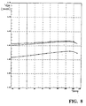
- Figures 8 and 9 show plots versus temperature of the parameter expressing the voltage difference Vds between the drain and source terminals of the PMOS transistors in the first pair 12 and the NMOS transistors in the second pair 12', respectively, as obtained from a suitable simulation carried out by the Applicant under different conditions tied to process variations.
- the substitutive circuit 11 of this invention allows the gains of both the first RX and the second TX data interface to be matched in a flexible manner compared to the transformers used in the prior art. In fact, this change in gain can be achieved by merely varying the resistances of the resistors used.
- the substitutive circuit 11 and the control and driving switch configuration 100 of this invention afford control over the loop current ILOOP and a limitation on the latter, by the added provision of dedicated circuits, such as the sensing resistor Rgnd, within the device.
- the foregoing expedients affecting both the first pair 12 of PMOS transistors and the second pair 12' of NMOS transistors can provide a low voltage drop, high transistor output impedance, and low current consumption by using components of the MOS type, thereby ensuring a low dissipated power which is constant with temperature and unaffected by process variations.
Landscapes
- Engineering & Computer Science (AREA)
- Computer Networks & Wireless Communication (AREA)
- Signal Processing (AREA)
- Logic Circuits (AREA)
- Dc Digital Transmission (AREA)
Claims (28)
- Circuit de remplacement de transistors MOS ayant une fonction de transformateur/d'interface de données, en particulier pour des réseaux RNIS, comportant des premier (11a) et second (11b) blocs d'alimentation/d'émission, ledit premier bloc d'alimentation/d'émission (11a) étant connecté entre une référence de tension (V) et une première interface de données (RX), et ledit second bloc d'alimentation/d'émission (11b) étant connecté entre une référence de potentiel de la masse (GND) et une seconde interface de données (TX), lesdits premier et second blocs d'alimentation/d'émission (11a, 11b) étant en outre connectés à une référence de tension d'alimentation (VDD), caractérisé en ce que le circuit de remplacement de transistors MOS comporte des première (12) et seconde (12') paires de transistors MOS respectivement connectés à ladite référence de tension (V), et à ladite référence de potentiel de la masse (GND), lesdits transistors MOS étant montés en diode et conservés dans leur plage de saturation, de manière à avoir une impédance en courant alternatif (AC) élevée et une impédance en courant continu (DC) quasiment égale à zéro, minimisant ainsi une dissipation d'énergie via ledit circuit de remplacement.
- Circuit de remplacement de transistors MOS selon la revendication 1, caractérisé en ce que ladite référence de tension (V) correspond soit à une tension de téléalimentation (VR) soit à une tension d'urgence (Vem), respectivement dans un premier état de fonctionnement ("état normal") caractérisé par la présence d'un signal de commande d'inversion de polarité (Scrp), et dans un second état ("état d'urgence RM") caractérisé par l'absence du signal de commande d'inversion de polarité (Scrp).
- Circuit de remplacement de transistors MOS selon la revendication 2, caractérisé en ce que les transistors (M1, M2 - M1', M2') desdites première et seconde paires (12, 12') sont montés en diode via des résistances de connexion respectives (R1, R2 - R1', R2') et sont adaptés pour faire passer le même courant DC qui circule à travers les fils de connexion dans les première et seconde interfaces de données (RX, TX).
- Circuit de remplacement de transistors MOS selon la revendication 3, caractérisé en ce que ledit second bloc d'alimentation/d'émission (11b) comporte le premier (M1') et le second transistor (M2') de la seconde paire (12'), lesdits transistors ayant leurs bornes de grille connectées en commun aux bornes de drain respectives via les première (R1') et seconde (R2') résistances de connexion de la seconde paire (12'), leurs bornes de source connectées à une référence de potentiel de la masse (GND), et leurs bornes de drain connectées à la seconde interface de données (TX).
- Circuit de remplacement de transistors MOS selon la revendication 4, caractérisé en ce que ledit second bloc d'alimentation/d'émission (11b) comporte en outre des premier (16'), deuxième (17'), troisième (20) et quatrième (21) miroirs de courant formant une connexion en pont entre la référence de tension d'alimentation (VDD) et la référence de potentiel de la masse (GND), en particulier, lesdits premier et deuxième miroirs de courant (16', 17') étant connectés à la référence de tension d'alimentation (VDD) et aux troisième et quatrième miroirs de courant (20, 21), eux-mêmes connectés à la référence de potentiel de la masse (GND).
- Circuit de remplacement de transistors MOS selon la revendication 5, caractérisé en ce que les premier et quatrième miroirs de courant (16', 21) sont connectés au premier transistor de la seconde paire (M1') via un premier élément de découplage (D1) et découplés de la seconde interface de données (TX) par un premier condensateur de découplage (C1'), alors que les deuxième et troisième miroirs de courant (17', 20) sont connectés au second transistor de la seconde paire (M2') via un second élément de découplage (D2) et découplés de la seconde interface de données (TX) par un second condensateur de découplage (C2'), lesdits éléments de découplage (D1, D2) étant utilisés dans des états particuliers d'alimentation dans le circuit de remplacement de transistors MOS.
- Circuit de remplacement de transistors MOS selon la revendication 5, caractérisé en ce que ledit second bloc d'alimentation/d'émission (11b) comporte en outre un tampon (22) connecté aux premier et troisième miroirs de courant (16', 20). via une première résistance de découplage (R5), et aux deuxième et quatrième miroirs de courant (17', 21) via une seconde résistance de découplage (R6).
- Circuit de remplacement de transistors MOS selon la revendication 7, caractérisé en ce que ledit tampon (22) est connecté entre la référence de tension d'alimentation (VDD) et la référence de potentiel de la masse (GND), et connecté à une référence de tension de référence (VREF), de manière à être adapté à une tension de référence de sortie (VREF) pour les miroirs de courant (16', 17', 20, 21), alors que les résistances de découplage (R5, R6) sont adaptées pour établir une impédance appropriée pour un signal AC présenté dans la seconde interface de données (TX).
- Circuit de remplacement de transistors MOS selon la revendication 5, caractérisé en ce que ledit second bloc d'alimentation/d'émission (11b) comporte en outre un convertisseur de tension/courant (15') ayant des première et seconde bornes d'entrée (C, D) et étant connecté auxdits premier et deuxième miroirs de courant (16', 17').
- Circuit de remplacement de transistors MOS selon la revendication 3, caractérisé en ce que ledit premier bloc d'alimentation/d'émission (11a) comporte le premier (M1) et le second transistor (M2) de la première paire (12), lesdits transistors ayant leurs bornes de grille connectées en commun et aux bornes de drain respectives via la première (R1) et la seconde (R2) résistance de connexion de la première paire (12), leurs bornes de source connectées à la référence de tension (V) et leurs bornes de drain connectées à la première interface de données (RX).
- Circuit de remplacement de transistors MOS selon la revendication 10, caractérisé en ce que ledit premier bloc d'alimentation/d'émission (11a) comporte en outre un convertisseur de tension/courant (15) connecté entre la référence de tension d'alimentation (VDD) et la référence de potentiel de la masse (GND), et connecté aux bornes de drain des transistors (M1, M2) via des premier (C1) et second (C2) condensateurs de découplage, respectivement, qui sont eux-mêmes connectés à une référence de tension de référence (VREF) via des première (R3) et seconde (R4) résistances de polarisation.
- Circuit de remplacement de transistors MOS selon la revendication 11, caractérisé en ce que ledit convertisseur de tension/courant (15) est en outre connecté à la référence de tension d'alimentation (VDD) via des premier (16) et deuxième (17) miroirs de courant du premier bloc d'alimentation/d'émission (11a).
- Circuit de remplacement de transistors MOS selon la revendication 12, caractérisé en ce que lesdits premier et deuxième miroirs de courant (16, 17) du premier bloc d'alimentation/d'émission (11a) sont connectés à un premier (18) et à un second (19) circuits amplificateurs, eux-mêmes connectés entre la référence de tension d'alimentation (VDD) et la référence de potentiel de la masse (GND) et connectés, en étant montés en cascade l'un avec l'autre, à une borne de commande (OUT) dudit premier bloc d'alimentation/d'émission (11a).
- Circuit de remplacement de transistors MOS selon la revendication 13, caractérisé en ce que lesdits premier et second circuits amplificateurs (18, 19) ont des bornes de sortie respectives (A, B), une tension de sortie de signal AC étant présente sur lesdites bornes, laquelle est proportionnelle à la tension de ligne dans la première interface de données (RX) et modulable de manière appropriée par l'intermédiaire desdits premier et deuxième miroirs de courant (16, 17) et de résistances intégrées dans les circuits amplificateurs (18, 19).
- Circuit de remplacement de transistors MOS selon la revendication 3, caractérisé en ce que les valeurs des première (R1, R1') et seconde (R2, R2') résistances de connexion sont les mêmes pour les première et seconde paires de transistors (M1, M2 et M1', M2'), respectivement, de manière à être adaptées pour éliminer au niveau de la borne de grille commune des paires de transistors respectives (12, 12'), tout signal différentiel dans les première et seconde interfaces de données (RX, TX), lesdites paires de transistors (12, 12') étant adaptées pour ainsi offrir une impédance élevée à des signaux différentiels.
- Circuit de remplacement de transistors MOS selon la revendication 3, caractérisé en ce qu'il comporte en outre un générateur de courant de compensation (Gcom) connecté via les résistances de connexion (R1, R2 - R1', R2') destiné à extraire et à injecter, respectivement, un courant de compensation (Icom) homogène avec la variation desdites résistances de connexion (R1, R2 - R1', R2') et, en conséquence, à obtenir une chute de tension constante via lesdites résistances de connexion (R1, R2 - R1', R2') efficace pour réduire en outre l'énergie dissipée via ledit circuit de remplacement.
- Circuit de remplacement de transistors MOS selon la revendication 16, caractérisé en ce qu'il comporte un premier transistor de compensation (M3) monté en série avec les résistances de connexion (R1, R2) connectées aux transistors de la première paire (M1, M2) et à la référence de tension (V), et ayant sa borne de grille connectée à sa borne de drain et au générateur de courant de compensation (Gcom), sa borne de drain connectée en outre à la borne de grille commune des transistors (M1, M2) de la première paire (12) via une première résistance appariée (RA), et sa borne de source connectée auxdites résistances de connexion (R1, R2), et un second transistor de compensation (M3') monté en série avec les résistances de connexion (R1', R2') connectées aux transistors de la seconde paire (M1', M2') et à la référence de potentiel de la masse (GND), et ayant sa borne de grille connectée à sa borne de drain et au générateur de courant de compensation (Gcom), sa borne de drain connectée en outre à la borne de grille commune des transistors (M1', M2') de la seconde paire (12') via une seconde résistance appariée (RB), et sa borne de source connectée auxdites résistances de connexion (R1', R2') connectées aux transistors de la seconde paire (M1', M2'), lesdits transistors de compensation (M3, M3') étant ainsi montés en diode et ayant une chute de tension qui est quasiment égale à une tension de seuil de transistor MOS (VT), de manière à compenser les tensions de seuil des transistors utilisés, par rapport aux variations de température et de processus.
- Circuit de remplacement de transistors MOS selon la revendication 17, caractérisé en ce que le premier transistor de compensation (M3) a sa borne de source connectée en outre à la référence de tension (V) via une série constituée de ladite première résistance appariée (RA) et d'un premier générateur de courant apparié (GA), et en ce que le second transistor de compensation (M3') a sa borne de source connectée en outre à la référence de potentiel de la masse (GND) via une série constituée de ladite seconde résistance appariée (RB) et d'un second générateur de courant apparié (GB), lesdits générateurs de courant (GA, GB) étant ainsi adaptés pour permettre aux tensions à travers les résistances de connexion (R1, R2 - R1', R2') des première et seconde paires (12, 12') d'être modulées via les résistances appariées respectives (RA, RB) pour un ajustement optimal, au stade de fabrication, dudit circuit de remplacement, une réduction supplémentaire de l'énergie dissipée, et une compensation inhérente des effets de variations de température et de processus sur la tension de seuil (VT) des transistors utilisés.
- Circuit de remplacement de transistors MOS selon la revendication 1, caractérisé en ce que lesdites première et seconde paires (12, 12') comportent des transistors MOS d'un premier et d'un second type (PMOS, NMOS), respectivement.
- Circuit de remplacement de transistors MOS selon la revendication 19, caractérisé en ce que lesdites première et seconde paires de transistors (12, 12') peuvent être construites à partir de composants de base disponibles à partir de technologies mélangées habituelles du type BCD.
- Circuit de remplacement de transistors MOS selon les revendications 17 et 19, caractérisé en ce que lesdits premier et second transistors de compensation (M3, M3') sont respectivement du même type que les transistors (M1, M2 - M1', M2') des première et seconde paires (12, 12').
- Circuit de remplacement de transistors MOS selon la revendication 4, caractérisé en ce que les bornes de source desdits premier (M1') et second (M2') transistors de la seconde paire (12') sont connectées à la référence de potentiel de la masse (GND) via une résistance de détection de courant (Rgnd).
- Dispositif de commutation de commande et d'attaque pour des circuits de transformateur/d'émetteur de données de remplacement dans une terminaison de réseau, en particulier pour un réseau RNIS, ladite terminaison de réseau incluant des premier (2) et second (3) convertisseurs connectés à une référence de potentiel de la masse (GND), ledit premier convertisseur (2) étant adapté pour délivrer une tension d'alimentation (VDD) et une tension d'urgence (Vem), et ledit second convertisseur (3) étant adapté pour délivrer une tension de téléalimentation (VR), caractérisé en ce que le dispositif de commutation de commande et d'attaque comporte au moins des premier (11) et second (11') circuits de remplacement de transistors MOS conformément à l'une quelconque des revendications précédentes, lesquels circuits sont respectivement adaptés pour fonctionner dans un premier état de fonctionnement ("état normal") de la terminaison de réseau caractérisé par la présence du signal de commande d'inversion de polarité (Scrp), et dans un second état de fonctionnement ("Etat d'urgence RM") de la terminaison de réseau caractérisé par l'absence du signal de commande d'inversion de polarité (Scrp).
- Dispositif de commande selon la revendication 23, caractérisé en ce que lesdits premier et second circuits de remplacement de transistors MOS (11, 11') sont connectés à une ligne de signaux (BUS1) sur laquelle un signal de commande d'inversion de polarité (Scrp) est présent, lequel est généré par le second convertisseur (3) de la terminaison de réseau, et sont connectés aux première et seconde interfaces de données (RX, TX).
- Dispositif de commande selon la revendication 24, caractérisé en ce que ledit premier circuit de remplacement de transistors MOS (11) comporte des premier et second blocs d'alimentation normaux (5, 7), ledit premier bloc d'alimentation normal (5) étant adapté pour recevoir ladite tension de téléalimentation (VR) provenant du second convertisseur (3) et étant connecté à la ligne de signaux (BUS1) via un premier inverseur logique (9) et à la première interface de données (RX), et ledit second bloc d'alimentation normal (7) étant connecté à la ligne de signaux (BUS1) via un second inverseur logique (10), et connecté à la seconde interface de données (TX).
- Dispositif de commande selon la revendication 25, caractérisé en ce que ledit second circuit de remplacement de transistors MOS (11') comporte des premier et second blocs d'alimentation d'urgence (4, 8), ledit premier bloc d'alimentation d'urgence (4) étant adapté pour recevoir ladite tension d'urgence (Vem) provenant du premier convertisseur (2) via un limiteur de courant (6), et étant connecté audit second bloc d'alimentation normal (7) et à la seconde interface de données (TX), et ledit second bloc d'alimentation d'urgence (8) étant connecté audit premier bloc d'alimentation normal (5) et à la première interface de données (RX).
- Dispositif de commande selon la revendication 26, caractérisé en ce que, dans le premier état ("état normal") de fonctionnement de la terminaison de réseau, la tension de téléalimentation (VR) est présente, laquelle tension circule à travers le premier bloc d'alimentation normal (5) jusqu'à la première interface de données (RX), et depuis la seconde interface de données (TX) jusqu'à la masse via le second bloc d'alimentation normal (7).
- Dispositif de commande selon la revendication 27, caractérisé en ce que, dans le second état ("état d'urgence RM") de fonctionnement de la terminaison de réseau, la tension d'urgence (Vem) est présente, et le signal de commande d'inversion de polarité (Scrp) présent sur la ligne de signaux (BUS1) active les blocs d'alimentation d'urgence (4, 8) et désactive les blocs d'alimentation normaux (5, 7) via lesdits premier et second inverseurs (9, 10).
Priority Applications (3)
| Application Number | Priority Date | Filing Date | Title |
|---|---|---|---|
| EP97830462A EP0903927B1 (fr) | 1997-09-23 | 1997-09-23 | Circuit de transistors MOS avec fonction transformateur/interface de données |
| DE69729447T DE69729447D1 (de) | 1997-09-23 | 1997-09-23 | MOS-Transistorenschaltung mit Transformator/Datenschnittstellenfunktion |
| US09/159,526 US6560333B1 (en) | 1997-09-23 | 1998-09-23 | MOS transistors substitute circuit having a transformer/data interface function, particularly for ISDN networks and corresponding control and driving switch configuration |
Applications Claiming Priority (1)
| Application Number | Priority Date | Filing Date | Title |
|---|---|---|---|
| EP97830462A EP0903927B1 (fr) | 1997-09-23 | 1997-09-23 | Circuit de transistors MOS avec fonction transformateur/interface de données |
Publications (2)
| Publication Number | Publication Date |
|---|---|
| EP0903927A1 EP0903927A1 (fr) | 1999-03-24 |
| EP0903927B1 true EP0903927B1 (fr) | 2004-06-09 |
Family
ID=8230777
Family Applications (1)
| Application Number | Title | Priority Date | Filing Date |
|---|---|---|---|
| EP97830462A Expired - Lifetime EP0903927B1 (fr) | 1997-09-23 | 1997-09-23 | Circuit de transistors MOS avec fonction transformateur/interface de données |
Country Status (3)
| Country | Link |
|---|---|
| US (1) | US6560333B1 (fr) |
| EP (1) | EP0903927B1 (fr) |
| DE (1) | DE69729447D1 (fr) |
Families Citing this family (7)
| Publication number | Priority date | Publication date | Assignee | Title |
|---|---|---|---|---|
| US6480510B1 (en) | 1998-07-28 | 2002-11-12 | Serconet Ltd. | Local area network of serial intelligent cells |
| US6956826B1 (en) | 1999-07-07 | 2005-10-18 | Serconet Ltd. | Local area network for distributing data communication, sensing and control signals |
| US6690677B1 (en) | 1999-07-20 | 2004-02-10 | Serconet Ltd. | Network for telephony and data communication |
| US6549616B1 (en) | 2000-03-20 | 2003-04-15 | Serconet Ltd. | Telephone outlet for implementing a local area network over telephone lines and a local area network using such outlets |
| AT409206B (de) * | 2000-03-22 | 2002-06-25 | Ericsson Ahead Comm Systems Gm | Schaltungsanordnung zur stromversorgung einer netz-abschlusseinheit |
| IL154234A (en) | 2003-01-30 | 2010-12-30 | Mosaid Technologies Inc | Method and system for providing dc power on local telephone lines |
| IL159838A0 (en) | 2004-01-13 | 2004-06-20 | Yehuda Binder | Information device |
Family Cites Families (8)
| Publication number | Priority date | Publication date | Assignee | Title |
|---|---|---|---|---|
| US3649769A (en) * | 1970-10-28 | 1972-03-14 | Gen Electric | Circuit for supplying direct current to a telephone line |
| US4173714A (en) * | 1977-06-03 | 1979-11-06 | Tie/Communications, Inc. | Communication circuit with combined power feed and data transmission over a phantom channel |
| GB2104330A (en) * | 1981-08-19 | 1983-03-02 | Texas Instruments Ltd | Improvements in or relating to amplifiers |
| CA1211241A (fr) * | 1984-04-30 | 1986-09-09 | Joseph W. Hingston | Circuit d'alimentation de ligne pour boucle de signaux numeriques |
| FR2614737B1 (fr) * | 1987-04-29 | 1989-06-09 | Cit Alcatel | Alimentation en energie electrique continue secourue avec une signalisation de l'etat de secours par inversion de polarite |
| IT1253679B (it) * | 1991-08-30 | 1995-08-22 | Sgs Thomson Microelectronics | Circuito di rispristino all'accensione di un circuito integrato aventeun consumo statico nullo. |
| EP0657995B1 (fr) * | 1993-12-07 | 1999-10-13 | STMicroelectronics S.r.l. | Etage de sortie à transistors de type mixte |
| DE69632580D1 (de) * | 1996-07-24 | 2004-07-01 | St Microelectronics Srl | Ausgabestufe für Speicheranlage und für Niederspannungsanwendungen |
-
1997
- 1997-09-23 DE DE69729447T patent/DE69729447D1/de not_active Expired - Lifetime
- 1997-09-23 EP EP97830462A patent/EP0903927B1/fr not_active Expired - Lifetime
-
1998
- 1998-09-23 US US09/159,526 patent/US6560333B1/en not_active Expired - Lifetime
Also Published As
| Publication number | Publication date |
|---|---|
| US6560333B1 (en) | 2003-05-06 |
| EP0903927A1 (fr) | 1999-03-24 |
| DE69729447D1 (de) | 2004-07-15 |
Similar Documents
| Publication | Publication Date | Title |
|---|---|---|
| US4431868A (en) | Solid state telephone line interface circuit with ringing capability | |
| US5329585A (en) | Subscriber line interface circuit for controlling AC and DC output impedance | |
| US5856758A (en) | Low distortion driver employing positive feedback for reducing power loss in output impedance that effectively matches the impedance of driven line | |
| US4514595A (en) | Active impedance line feed circuit | |
| AU644162B2 (en) | Telecommunications line circuit | |
| AU707018B2 (en) | A transmission method | |
| US4203009A (en) | Unbalanced/balanced converter circuits | |
| US4797904A (en) | Transmitter for ISDN S-bus interface circuit | |
| EP0903927B1 (fr) | Circuit de transistors MOS avec fonction transformateur/interface de données | |
| CA1292588C (fr) | Circuit d'interface pour ligne d'abonne | |
| US5274702A (en) | Wideband telephone line interface circuit | |
| US4232293A (en) | Line interface unit for voice and wide band signal coupling | |
| US5661794A (en) | Telephone line interface circuit with voltage control | |
| US5940498A (en) | Electronic voice circuit configuration | |
| US5528688A (en) | Telephone battery feed circuit including noise reduction circuit | |
| US5343520A (en) | Impedance synthesis multile loop using filtering means | |
| GB2071461A (en) | Telephone line feed | |
| US4538032A (en) | Interface circuit with impedance adaptation means | |
| US4115660A (en) | Telephone line interfacing circuit with directional transfer of ringing current and off-hook indications | |
| JPS63155931A (ja) | デジタル信号伝送回路 | |
| US4361732A (en) | Trunk interface circuit with current compensation | |
| US20100124326A1 (en) | Subscriber line interface circuitry with common base audio isolation stage | |
| JPH08307523A (ja) | 加入者回線インタフェース回路、およびその内部に複数個のリンガを同時に駆動できるリング信号を生じる方法 | |
| KR100408746B1 (ko) | 직류전압및교류전압디커플링용회로장치 | |
| EP0096473B1 (fr) | Circuit d'alimentation de ligne à impédance active |
Legal Events
| Date | Code | Title | Description |
|---|---|---|---|
| PUAI | Public reference made under article 153(3) epc to a published international application that has entered the european phase |
Free format text: ORIGINAL CODE: 0009012 |
|
| AK | Designated contracting states |
Kind code of ref document: A1 Designated state(s): DE FR GB IT |
|
| AX | Request for extension of the european patent |
Free format text: AL;LT;LV;RO;SI |
|
| 17P | Request for examination filed |
Effective date: 19990622 |
|
| AKX | Designation fees paid |
Free format text: DE FR GB IT |
|
| GRAP | Despatch of communication of intention to grant a patent |
Free format text: ORIGINAL CODE: EPIDOSNIGR1 |
|
| GRAS | Grant fee paid |
Free format text: ORIGINAL CODE: EPIDOSNIGR3 |
|
| GRAA | (expected) grant |
Free format text: ORIGINAL CODE: 0009210 |
|
| AK | Designated contracting states |
Kind code of ref document: B1 Designated state(s): DE FR GB IT |
|
| REG | Reference to a national code |
Ref country code: GB Ref legal event code: FG4D |
|
| REF | Corresponds to: |
Ref document number: 69729447 Country of ref document: DE Date of ref document: 20040715 Kind code of ref document: P |
|
| PG25 | Lapsed in a contracting state [announced via postgrant information from national office to epo] |
Ref country code: DE Free format text: LAPSE BECAUSE OF FAILURE TO SUBMIT A TRANSLATION OF THE DESCRIPTION OR TO PAY THE FEE WITHIN THE PRESCRIBED TIME-LIMIT Effective date: 20040910 |
|
| ET | Fr: translation filed | ||
| PLBE | No opposition filed within time limit |
Free format text: ORIGINAL CODE: 0009261 |
|
| STAA | Information on the status of an ep patent application or granted ep patent |
Free format text: STATUS: NO OPPOSITION FILED WITHIN TIME LIMIT |
|
| 26N | No opposition filed |
Effective date: 20050310 |
|
| PGFP | Annual fee paid to national office [announced via postgrant information from national office to epo] |
Ref country code: GB Payment date: 20060905 Year of fee payment: 10 |
|
| PGFP | Annual fee paid to national office [announced via postgrant information from national office to epo] |
Ref country code: IT Payment date: 20060930 Year of fee payment: 10 |
|
| GBPC | Gb: european patent ceased through non-payment of renewal fee |
Effective date: 20070923 |
|
| REG | Reference to a national code |
Ref country code: FR Ref legal event code: ST Effective date: 20080531 |
|
| PG25 | Lapsed in a contracting state [announced via postgrant information from national office to epo] |
Ref country code: FR Free format text: LAPSE BECAUSE OF NON-PAYMENT OF DUE FEES Effective date: 20071001 |
|
| PGFP | Annual fee paid to national office [announced via postgrant information from national office to epo] |
Ref country code: FR Payment date: 20060928 Year of fee payment: 10 |
|
| PG25 | Lapsed in a contracting state [announced via postgrant information from national office to epo] |
Ref country code: GB Free format text: LAPSE BECAUSE OF NON-PAYMENT OF DUE FEES Effective date: 20070923 |
|
| PG25 | Lapsed in a contracting state [announced via postgrant information from national office to epo] |
Ref country code: IT Free format text: LAPSE BECAUSE OF NON-PAYMENT OF DUE FEES Effective date: 20070923 |