EP0903927B1 - MOS-Transistorenschaltung mit Transformator/Datenschnittstellenfunktion - Google Patents
MOS-Transistorenschaltung mit Transformator/Datenschnittstellenfunktion Download PDFInfo
- Publication number
- EP0903927B1 EP0903927B1 EP97830462A EP97830462A EP0903927B1 EP 0903927 B1 EP0903927 B1 EP 0903927B1 EP 97830462 A EP97830462 A EP 97830462A EP 97830462 A EP97830462 A EP 97830462A EP 0903927 B1 EP0903927 B1 EP 0903927B1
- Authority
- EP
- European Patent Office
- Prior art keywords
- substitutive
- voltage
- mos transistors
- transistors
- supply
- Prior art date
- Legal status (The legal status is an assumption and is not a legal conclusion. Google has not performed a legal analysis and makes no representation as to the accuracy of the status listed.)
- Expired - Lifetime
Links
- 239000003990 capacitor Substances 0.000 claims description 14
- 101100004933 Arabidopsis thaliana CYP79F1 gene Proteins 0.000 claims description 7
- 238000004519 manufacturing process Methods 0.000 claims description 6
- 238000000034 method Methods 0.000 claims description 5
- 230000008569 process Effects 0.000 claims description 5
- 230000000694 effects Effects 0.000 claims description 3
- 238000005516 engineering process Methods 0.000 claims description 3
- 230000009467 reduction Effects 0.000 claims description 3
- 230000005540 biological transmission Effects 0.000 description 11
- 238000010586 diagram Methods 0.000 description 6
- 239000008186 active pharmaceutical agent Substances 0.000 description 4
- 230000021715 photosynthesis, light harvesting Effects 0.000 description 3
- 230000009471 action Effects 0.000 description 2
- 230000006872 improvement Effects 0.000 description 2
- 241000607479 Yersinia pestis Species 0.000 description 1
- 230000003321 amplification Effects 0.000 description 1
- 230000008859 change Effects 0.000 description 1
- 238000006243 chemical reaction Methods 0.000 description 1
- 230000003247 decreasing effect Effects 0.000 description 1
- 230000001419 dependent effect Effects 0.000 description 1
- 230000009977 dual effect Effects 0.000 description 1
- 230000008030 elimination Effects 0.000 description 1
- 238000003379 elimination reaction Methods 0.000 description 1
- 238000005265 energy consumption Methods 0.000 description 1
- 238000003199 nucleic acid amplification method Methods 0.000 description 1
- 238000004088 simulation Methods 0.000 description 1
- 238000004804 winding Methods 0.000 description 1
Images


Classifications
-
- H—ELECTRICITY
- H04—ELECTRIC COMMUNICATION TECHNIQUE
- H04Q—SELECTING
- H04Q11/00—Selecting arrangements for multiplex systems
- H04Q11/04—Selecting arrangements for multiplex systems for time-division multiplexing
- H04Q11/0428—Integrated services digital network, i.e. systems for transmission of different types of digitised signals, e.g. speech, data, telecentral, television signals
- H04Q11/0435—Details
-
- H—ELECTRICITY
- H04—ELECTRIC COMMUNICATION TECHNIQUE
- H04L—TRANSMISSION OF DIGITAL INFORMATION, e.g. TELEGRAPHIC COMMUNICATION
- H04L12/00—Data switching networks
-
- H—ELECTRICITY
- H04—ELECTRIC COMMUNICATION TECHNIQUE
- H04M—TELEPHONIC COMMUNICATION
- H04M19/00—Current supply arrangements for telephone systems
- H04M19/08—Current supply arrangements for telephone systems with current supply sources at the substations
-
- H—ELECTRICITY
- H04—ELECTRIC COMMUNICATION TECHNIQUE
- H04Q—SELECTING
- H04Q2213/00—Indexing scheme relating to selecting arrangements in general and for multiplex systems
- H04Q2213/13003—Constructional details of switching devices
-
- H—ELECTRICITY
- H04—ELECTRIC COMMUNICATION TECHNIQUE
- H04Q—SELECTING
- H04Q2213/00—Indexing scheme relating to selecting arrangements in general and for multiplex systems
- H04Q2213/1308—Power supply
-
- H—ELECTRICITY
- H04—ELECTRIC COMMUNICATION TECHNIQUE
- H04Q—SELECTING
- H04Q2213/00—Indexing scheme relating to selecting arrangements in general and for multiplex systems
- H04Q2213/13082—Power supply via phantom line
-
- H—ELECTRICITY
- H04—ELECTRIC COMMUNICATION TECHNIQUE
- H04Q—SELECTING
- H04Q2213/00—Indexing scheme relating to selecting arrangements in general and for multiplex systems
- H04Q2213/1309—Apparatus individually associated with a subscriber line, line circuits
-
- H—ELECTRICITY
- H04—ELECTRIC COMMUNICATION TECHNIQUE
- H04Q—SELECTING
- H04Q2213/00—Indexing scheme relating to selecting arrangements in general and for multiplex systems
- H04Q2213/13166—Fault prevention
-
- H—ELECTRICITY
- H04—ELECTRIC COMMUNICATION TECHNIQUE
- H04Q—SELECTING
- H04Q2213/00—Indexing scheme relating to selecting arrangements in general and for multiplex systems
- H04Q2213/13202—Network termination [NT]
-
- H—ELECTRICITY
- H04—ELECTRIC COMMUNICATION TECHNIQUE
- H04Q—SELECTING
- H04Q2213/00—Indexing scheme relating to selecting arrangements in general and for multiplex systems
- H04Q2213/13209—ISDN
-
- H—ELECTRICITY
- H04—ELECTRIC COMMUNICATION TECHNIQUE
- H04Q—SELECTING
- H04Q2213/00—Indexing scheme relating to selecting arrangements in general and for multiplex systems
- H04Q2213/13305—Transistors, semiconductors in general
-
- H—ELECTRICITY
- H04—ELECTRIC COMMUNICATION TECHNIQUE
- H04Q—SELECTING
- H04Q2213/00—Indexing scheme relating to selecting arrangements in general and for multiplex systems
- H04Q2213/1332—Logic circuits
-
- H—ELECTRICITY
- H04—ELECTRIC COMMUNICATION TECHNIQUE
- H04Q—SELECTING
- H04Q2213/00—Indexing scheme relating to selecting arrangements in general and for multiplex systems
- H04Q2213/13322—Integrated circuits
-
- Y—GENERAL TAGGING OF NEW TECHNOLOGICAL DEVELOPMENTS; GENERAL TAGGING OF CROSS-SECTIONAL TECHNOLOGIES SPANNING OVER SEVERAL SECTIONS OF THE IPC; TECHNICAL SUBJECTS COVERED BY FORMER USPC CROSS-REFERENCE ART COLLECTIONS [XRACs] AND DIGESTS
- Y02—TECHNOLOGIES OR APPLICATIONS FOR MITIGATION OR ADAPTATION AGAINST CLIMATE CHANGE
- Y02D—CLIMATE CHANGE MITIGATION TECHNOLOGIES IN INFORMATION AND COMMUNICATION TECHNOLOGIES [ICT], I.E. INFORMATION AND COMMUNICATION TECHNOLOGIES AIMING AT THE REDUCTION OF THEIR OWN ENERGY USE
- Y02D30/00—Reducing energy consumption in communication networks
- Y02D30/70—Reducing energy consumption in communication networks in wireless communication networks
Definitions
- This invention relates to a MOS transistors substitutive circuit having a transformer/data interface function, particularly for ISDN networks, and corresponding control and driving switch configuration.
- the invention relates to a MOS transistors substitutive circuit having a transformer/data interface function, particularly for ISDN networks, which circuit comprises first and second power supply/transmitter blocks, said first power supply/transmitter block being connected between a voltage reference and a first data interface, and said second power supply/transmitter block being connected between a ground potential reference and a second data interface, said first and second power supply/transmitter blocks being further connected to a supply voltage reference.
- the invention also relates to a control and driving switch configuration for substitutive transformer/data transmitter circuits in a network termination, in particular ISDN network terminations, said network termination including first and second converters connected to a ground potential reference, said first converter delivering a supply voltage and an emergency voltage and said second converter delivering a remote supply voltage.
- the invention particularly, but not exclusively, concerns an ISDN network termination, and the description that follows will make reference to that application for simplicity of illustration.
- An important additional function is, besides voice transmission, the transmission of information relating to new products and/or services, such as facsimile operations, video communications, network interconnections, etc..
- the transmission of data by a telephone terminal unit may utilize special networks.
- One example of a well known and widely utilized network is the ISDN (Integrated Services Digital Network), originating by natural evolution from the traditional telephone network and employing the same standard cables. This compatibility of transmission with the traditional telephone network allows the ISDN network to use the so-called telephone loops, which are advantageously available throughout the territory.
- ISDN Integrated Services Digital Network
- the ISDN network is to European standard, having a transmit rate of 64 kbit/sec; the ISDN network allows two talk channels plus a control and service channel to be sent over the same line, which channels can be either used by two telephone sets, or one telephone set and a facsimile, or one telephone set and a PC (Personal Computer).
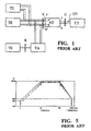
- Figure 1 Shown by way of example in Figure 1 is a block diagram for basic access to the ISDN network. This diagram is also shown in Figure 2, in greater detail.
- FIG. 1 Also shown in Figure 1 are first U, second S and third R reference points, whereat special interface circuits are connected, as detailed in Figure 2 for the references U and S only.
- the line termination LT provides for power supply in the remote mode to the network termination NT, and in an emergency condition known in the art as RM (Restricted Mode), for a terminal apparatus TE as well.
- RM Remote Mode
- the line termination LT allows signal data DS to be transmitted and received in suitable formats, such as the 2B1Q or 4B3T formats, through the interface circuits of the reference point U.
- the terminal adapter TA connected in the reference point R, allows apparatus designed for different data transmission modes, usually commercially available apparatus, to be also connected to the network termination NT.
- the network termination NT is connected to the line termination LT by a two-wire telephone loop, whereby the network termination NT can be powered from the line termination LT and can exchange with it data DS simultaneously in either directions.
- the network termination NT is provided with a DC/DC converter CONV1 capable of delivering a supply voltage VDD, typically of 5V, to the interface circuits at the reference points U and S, as well as an emergency voltage Vem.
- VDD supply voltage
- Vem emergency voltage
- the emergency voltage Vem of about 40V, can only be used in an RM emergency condition to power the terminal apparatus TE, with some suitable constraints.
- Such terminal apparatus TE are normally powered from an AC/DC converter CONV2 provided at the network termination NT and capable of powering up to eight terminal apparatuses TE, according to the standard applied.
- the emergency voltage Vem is disconnected by means of a first switch arrangement SW, shown in Figure 2, which is closed at the AC/DC converter CONV2.
- the network termination NT has two input terminals A, B and four output terminals A', A'' and B', B'', two for each transformer of the interface circuit at the reference point S, as previously shown schematically in Figure 1.
- the output terminals A', A'' and B', B'' provide for remote power supply and data transmission through a supply/data transmission block BT comprising a DC/DC converter CONV3, a transmit block TX', and a receive block RX', so as to communicate with the terminal apparatus TE.
- the transmit and receive blocks, TX', RX' are schematically represented in Figure 2 by simple transformers serving to receive the power supply and allow of the data, present in the transmit and receive blocks TX', RX', conversion.
- power to the terminal apparatus TE is supplied from the interface circuits at the reference point S by means of the transformers, shown schematically in Figure 2, which are also utilized for exchanging the signal data DS.
- These transformers allow a virtually zero DC voltage drop to be obtained, and have an AC impedance which is a function of load and the winding ratio of the transformer.
- the supply to the terminal apparatus TE under RM emergency conditions is controlled through the switches SW.
- the combination of the transformers in the interface circuits at the reference point S and the switches SW controlling the supply to the terminal apparatus TE form a transformer/data interface/switch circuit for effecting a polarity reversal CT according to the prior art.
- transformers for powering or effecting the exchange of signal data DS at the interface circuits, is specially convenient from the standpoint of energy dissipation. Minimizing energy dissipation is highly important under RM emergency conditions; in such circumstances, in fact, no mains supply would be available, and the available power would be limited to the small power that the DC/DC converter at the interface circuits of the reference point U can draw on the line.
- transformers must be designed to meet specific applicational requirements, thereby producing a manufacturing cost.
- circuits including active components are described in US Patents No. 3,649,769 to Pest, No. 4,004,104 to Picandet et al., No. 3,943,432 to Colardelle et al., and No. 4,088,843 to Rogers et al..
- the prior art active component circuits are less expensive than transformers. But they are unsatisfactory from the energy dissipation standpoint, and still require suitable switches for supply control.
- the underlying technical problem of this invention is to provide a transformer/data interface circuit emulating a transformer for an ISDN telephone line, which can transmit the data presented on the line, transmit and control the power supply to the terminal apparatus (reversal of current polarity or direction), and has suitable structural and functional features to afford reduced energy consumption and overcome the drawbacks that are still besetting the prior art devices.
- circuits comprising MOS transistors which operate in the saturation range, and are suitably configured as diodes through common resistors, substitutes the transformer/data interface/switch circuit comprising the combined transformers and power supply control switches as provided at the network termination in the prior art, so as to present a high A.C. impedance and virtually zero D.C. impedance, thus minimizing the overall dissipation of power by the network termination, and allowing the power supply to be controlled under any conditions of operation of the network termination, while effecting the reversal in the current direction.
- control and driving switch configuration for substitutive transformer/data transmitter circuits in a network termination, as previously indicated and defined in the characterizing part of Claim 23.
- the control configuration selects the voltage reference to be applied to the power supply/transmitter blocks.
- FIG. 1 generally and schematically shown at 1 is a network termination according to the invention, wherein the transmission of data is not illustrated.
- Figure 3 illustrates in particular a power supply distribution through the network termination 1, comprising first 2 and second 3 converters, specifically a DC/DC converter and an AC/DC converter.
- the architecture of the network termination 1 of Figure 3 may also be used for data transmission.
- the first DC/DC converter 2 is connected to a ground potential reference GND, and delivers a supply voltage VDD, e.g. of either 5V or 3.3V, and an emergency voltage Vem, typically of 40V, similar to the DC/DC converter CONV1 described above in connection with the prior art.
- the second AC/DC converter 3 is connected to the ground potential reference GND and issues a polarity reversal control signal Scrp and a remote supply voltage VR, typically of 48V, on a signal line BUS1.
- the first 2 and second 3 converters are also connected to a first RM emergency condition supply block 4 and a second normal condition supply block 5, respectively, comprising P-channel MOS or PMOS transistors.
- a current limiter 6 which is set, for example, to a value in the 9mA to 11mA range, harmonizing with regulations.
- the first 4 and second 5 supply blocks are connected to a third normal condition supply block 7 and a fourth RM emergency condition supply block 8, respectively, which comprise N-channel MOS or NMOS transistors.
- the third 7 and fourth 8 supply blocks are also connected to the ground potential reference GND.
- first 4 and fourth 8 supply blocks are connected directly to the signal line BUS1, while the second 5 and third 7 supply blocks are connected thereto through first 9 and second 10 logic inverters.
- the second 5 and fourth 8 supply blocks are connected to a first data interface RX, and the first 4 and third 7 supply blocks are connected to a second data interface TX.
- the block RL schematically shown in Figure 3 as being connected to the data interfaces RX and TX, represents an equivalent DC resistor of a power supply/data transmission receive block connected to these interfaces and needed by the terminal apparatus TE.
- the network termination 1 comprises first 11 and second 11' MOS transistors substitutive circuits having a transformer/data interface function, respectively comprising normal condition supply blocks 5, 7 and RM emergency condition supply blocks 4, 8.
- the emergency voltage Vem and remote supply voltage VR are respectively applied to the supply blocks 5, 7 and 4, 8 in a first condition of operation, referred to as the normal operation condition, and in a second condition of operation, referred to as the emergency condition, of the network termination 1.
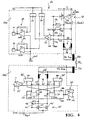
- a MOS transistors substitutive circuit having a transformer/data interface function, according to the invention, is shown best in Figure 4.
- the substitutive circuit 11 comprises first 11a and second 11b power supply/transmitter blocks, which essentially correspond to the first supply block 4 in the RM emergency condition, or to the second supply block 5 in the normal condition, and to the fourth supply block 8 in the RM emergency condition, or the third supply block 7 in the normal condition, respectively.
- This substitutive circuit 11 is implemented by a first pair 12 of P-channel MOS or PMOS transistors, and a second pair 12' of N-channel MOS or NMOS transistors.
- the transistors of each pair 12, 12' draw the same DC current in the connection leads to the first RX and second TX data interfaces.
- first 12 and second 12' MOS transistor pairs are easily constructed from basic components made available by conventional mixed technologies of the BCD type.
- FIG. 4 shows that either (respectively PMOS and NMOS) transistor pairs 12, 12' are diode connected through suitable connection resistors.
- the first transistor pair 12 of the first power supply/transmitter block 11a comprises first M1 and second M2 P-channel transistors which are connected to a voltage reference V corresponding either to the remote supply voltage VR or the emergency voltage Vem, according to the operation condition of the network termination whereto the substitutive transformer/data interface circuit 11 is incorporated.
- the first M1 and second M2 transistors are also connected to the first data interface RX, and have their gate terminals in common and connected to the respective drain terminals through first R1 and second R2 connection resistors.
- the drain terminals of the transistors M1 and M2 are connected to the first data interface RX through a suitable decoupling circuit 13 which comprises at least one cross-connection resistor 14 and suitable common mode inductors.
- the drain terminals of the transistors M1 and M2 are also connected to a voltage/current converter 15 through first C1 and second C2 decoupling capacitors, respectively, which capacitors are further connected to a reference voltage reference VREF through first R3 and second R4 bias resistors.
- the voltage/current converter 15 is connected between the supply voltage reference VDD and the ground potential reference GND, and further connected to the supply voltage reference VDD via first 16 and second 17 current mirrors.
- the first 16 and second 17 current mirrors are connected to first 18 and second 19 amplifier circuits which are connected between the supply voltage reference VDD and the ground potential reference GND and connected, in parallel with each other, to a control terminal OUT whereat a voltage value equal to one half the supply voltage VDD is present.
- an output voltage which is proportional to the voltage present on the line, limited to the conditions of the signal AC; this output voltage can be modulated by means of the current mirrors 16 and 17 and the resistors included in the amplifier circuits 18 and 19.
- the second transistor pair 12' of the second power supply/transmitter block 11b comprises first M1' and second M2' N-channel transistors being connected between the ground potential reference GND and the second data interface TX and having their gate terminals in common and connected to the respective drain terminals through first R1' and second R2' connection resistors.
- the first M1' and second M2' transistors have their source terminals in common and connected, through a suitable sensing resistor Rgnd (unessential to the aim of the invention), to the ground potential reference GND, and have their drain terminals connected to first D1 and second D2 decoupling elements, e.g. two diodes, and connected to the second data interface TX via a suitable decoupling circuit 13' which comprises at least one cross-connection resistor 14' and suitable common mode inductors.
- drain terminals of the transistors M1' and M2' are also connected, through the decoupling elements D1 and D2, to first 16' and second 17' current mirrors which are further connected to the supply voltage reference VDD and decoupled from the second data interface TX by means of first C1' and second C2' decoupling capacitors.
- the decoupling elements D1 and D2 operate in particular supply conditions of the substitutive circuit 11.
- the first C1' and second C2' decoupling capacitors are also connected to the ground potential reference GND through third 20 and fourth 21 current mirrors.
- the first 16' and second 17' current mirrors are connected to both the third 20 and fourth 21 current mirrors in crossed manner, thereby forming a "bridge" connection.
- the first 16' and second 17' current mirrors are also connected to a buffer circuit 22 through first R5 and second R6 decoupling resistors, respectively, and connected to a voltage/current converter 15' which has first C and second D input terminals.
- the buffer 22 is connected between the supply voltage reference VDD and the ground potential reference GND, and connected to the reference voltage reference VREF.
- the buffer 22 sets the output reference voltage VREF for the current mirrors 16', 17', 20 and 21.
- the decoupling resistors R5 and R6 will then establish an impedance between the current mirrors 17', 21 and 16', 20, respectively, suitable to provide, in a condition of AC current, a higher impedance value than the resistance value of the cross-connection 14' in the decoupling circuit 13'.
- the buffer 22 thus will, in cooperation with the decoupling resistors R5 and R6, set the working voltage of the current mirrors without altering the line impedance value across the cross-connection resistor 14'.
- the reference voltage VREF is one half the supply voltage VDD.
- a differential data signal specifically a voltage, presented across the cross-connection resistor 14 of the decoupling circuit 13 associated with the first data interface RX, will "see” a high impedance through the transistors M1 and M2, and especially through the parallel connection of the resistors R1, R2, R3 and R4.
- This differential data signal then travels through the decoupling capacitors C1 and C2 to the voltage/current converter 15, where it is converted to a current.
- the differential current data signal then goes through the current mirrors 16 and 17 to be ultimately converted back to a voltage by the amplifier circuits 18 and 19.
- the differential data signal associated with the first data interface RX will again be presented, suitably amplified, at the output terminals A and B of the amplifier circuits 18 and 19.
- the final amplification value of the differential data signal can be programmed by varying the ratio of the current mirrors 16, 17 and the resistance values used.
- a differential data signal such as a voltage
- a differential data signal at the input terminals C and D of the voltage/current converter 15' in the second power supply/transmitter block 11b is converted to a current and transmitted to the bridge configuration of the current mirrors 16', 17', 20 and 21.
- the differential data signal converted to a current has a first polarity, it is input, through the decoupling capacitor C1' connected to the first current mirror 16', to a first terminal of the cross-connection resistor 14' of the decoupling circuit 13' associated with the second data interface TX, to then loop back to ground through the decoupling capacitor C2' and the fourth current mirror 21.
- the second power supply/transmitter block 11b can be said to replicate, at the second data interface TX, the differential data signal presented to the input of the voltage/current converter 15'.
- This differential data signal is output with said first polarity.
- the differential current data signal has a second polarity, in particular a reversed polarity form the first, it is input, through the decoupling capacitor C2' connected to the second current mirror 17', to a second terminal of the cross-connection resistor 14' of the decoupling circuit 13' associated with the second data interface TX, to then loop back to ground through the decoupling capacitor C1' and the third current mirror 20.
- connection to the cross-connection resistor 14' is the reverse from the previously discussed differential data signal having a first polarity, and the second power supply/transmitter block 11b will replicate the differential data signal, presented to the input of the voltage/current converter 15' and having said second polarity, at the second data interface TX.
- the transistors M1 and M2 would offer, in fact, a low resistance to the passage of said supply current.
- the mid-point terminal of the interface transformers in the first data interface RX is suitably connected to the mid-point terminal of the interface transformers in the second data interface TX, thereby allowing the supply current to cross the decoupling circuit 13'.
- the equivalent resistance of this connection is schematically represented by the block RL in Figure 4.
- the supply current path then loops back to ground through the transistors M1' and M2'.
- MOS transistors substitutive circuit of the invention replaces, therefore, the transformers associated with the interface at the reference point S in the prior art.
- the polarity reversal control signal Scrp on the signal line BUS1 will activate the emergency condition supply blocks 4, 8 (connected to the emergency voltage Vem of about 40V), and simultaneously deactivate the normal condition supply blocks 5, 7 by means of the inverters 9 and 10.
- this control on the supply distribution for the normal and emergency conditions is effected through the transistors of the substitutive circuits 11 and 11'.
- these transistors are either connected to the remote supply voltage VR outgoing from the AC/DC converter 3 or the emergency voltage Vem, to activate and deactivate operation of the first and second supply blocks 5, 7 in the normal operation condition, or operation of the first and second supply blocks 4, 8 in the RM emergency condition.
- control and driving switch configuration comprised of a pair of MOS transistors substitutive circuits according to the invention, thus replaces functionally the switches SW of the prior art.
- a filter capacitor between the common gate terminal and the source terminal of the transistors in the first 12 and second 12' pairs of MOS transistors.
- Such a filter capacitor may be used, however, in case of any mismatching of the resistors, in order to increase the output impedances of the MOS transistor pairs 12 and 12'.
- an overall impedance value Z must be in agreement with the graph of Figure 5.
- This graph is taken from Specification ITU-T I430 and fixes an impedance value of more than 2.5 kOhm in the frequency range of 20kHz to 1106kHz.
- the impedance for the second power supply/transmitter block 11b can be similarly computed.
- the latter takes a value equal to the threshold voltage value VT plus an overdrive voltage dependent on the current ILOOP.
- a basic requirement of the substitutive circuit 11 with transformer function is that the dissipated power Pdiss be minimized. It is therefore necessary to keep the voltage difference Vds between the drain and source terminals of the MOS transistors employed as low as congruous with the above impedance requirements.
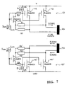
- a first action toward minimizing the power dissipated through the MOS pairs is to extract or inject an appropriate compensation current Icom (homogeneous with the variations in the connection resistors R1, R2 and R1', R2') so as to obtain a constant voltage drop across these connection resistors R1,R2 and R1', R2' forming the diode connection, which should then be subtracted from the voltage Vds, as shown schematically in Figure 6 in relation to the first 12 and second 12' diode-configured transistor pairs only.
- Icom homogeneous with the variations in the connection resistors R1, R2 and R1', R2'
- This action can be easily implemented by having a suitable compensation current generator Gcom connected across the connection resistors R1, R2 and R1', R2'.
- a MOS component of the same type as the transistors used in the PMOS pair 12 and NMOS pair 12' is advantageously provided, in series with the connection resistors R1, R2 and R1', R2' forming the diode connections of transistors M1, M2 and M1', M2'.
- first M3 and second M3' compensation transistors are included, as schematically shown in Figure 7.
- the first compensation transistor M3 has its gate terminal connected to its drain terminal, and connected to the compensation current generator Gcom, its drain terminal being further connected to the common gate terminal of the first M1 and second M2 transistors in the pair 12 through a first matching resistor RA, and connected to the voltage reference V through a first match current generator GA; the transistor source terminal being connected to the connection resistors R1 and R2.
- the second compensation transistor M3' has its gate terminal connected to its drain terminal, and connected to the compensation current generator Gcom, its drain terminal being further connected to the common gate terminal of the first M1' and second M2' transistors in the pair 12' through a second matching resistor RB, and connected to the ground reference GND through a second match current generator GB; the transistor source terminal being connected to the connection resistors R1' and R2'.
- the transistors M3 and M3' are in a diode configuration, and have a voltage drop which is virtually the same as VT.
- the additional resistors RA and RB and their associated current generators GA and GB allow the voltages across the connection resistors R1, R2 and R1', R2' to be modulated for optimum adjustment at the manufacturing stage of the substitutive circuit 11.
- the voltage Vds at the MOS transistor pairs 12 and 12' can be significantly reduced, resulting in a reduction of the power Pdiss dissipated through the substitutive circuit 11.
- a further contribution to reducing the voltage drop Vds across each of the MOS transistor pairs 12, 12' may also come from a suitable dimensioning of the individual transistors M1, M2 and M1', M2' in the pairs 12 and 12'.
- the voltage Vds can be decreased, while being careful, however, to keep the transistors M1, M2 and M1', M2' within their saturation range, for best compromise size/dissipated power.
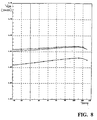
- Figures 8 and 9 show plots versus temperature of the parameter expressing the voltage difference Vds between the drain and source terminals of the PMOS transistors in the first pair 12 and the NMOS transistors in the second pair 12', respectively, as obtained from a suitable simulation carried out by the Applicant under different conditions tied to process variations.
- the substitutive circuit 11 of this invention allows the gains of both the first RX and the second TX data interface to be matched in a flexible manner compared to the transformers used in the prior art. In fact, this change in gain can be achieved by merely varying the resistances of the resistors used.
- the substitutive circuit 11 and the control and driving switch configuration 100 of this invention afford control over the loop current ILOOP and a limitation on the latter, by the added provision of dedicated circuits, such as the sensing resistor Rgnd, within the device.
- the foregoing expedients affecting both the first pair 12 of PMOS transistors and the second pair 12' of NMOS transistors can provide a low voltage drop, high transistor output impedance, and low current consumption by using components of the MOS type, thereby ensuring a low dissipated power which is constant with temperature and unaffected by process variations.
Landscapes
- Engineering & Computer Science (AREA)
- Computer Networks & Wireless Communication (AREA)
- Signal Processing (AREA)
- Logic Circuits (AREA)
- Dc Digital Transmission (AREA)
Claims (28)
- MOS-Transistor-Ersatzschaltung mit einer Übertrager-/Datenschnittstellen-Funktion, insbesondere für ISDN-Netzwerke, umfassend einen ersten (11a) und einen zweiten (11b) Spannungsversorgungs/Senderblock, von denen der erste Spannungsversorgungs-Senderblock (11a) zwischen eine Referenzspannung (V) und eine erste Datenschnittstelle (RX) geschaltet ist und der zweite Spannungsversorgungs/Senderblock (11b) zwischen Masse-Referenzpotential (GND) und eine zweite Datenschnittstelle (TX) geschaltet ist, der erste und der zweite Spannungsversorgungs-Senderblock (11a, 11b) weiterhin an eine Versorgungs-Referenzspannung (VDD) angeschlossen sind, dadurch gekennzeichnet, dass die MOS-Transistor-Ersatzschaltung aufweist: ein erstes (12) und ein zweites (12') MOS-Transistorpaar, die an die Referenzspannung (V) bzw. an das Massereferenzpotential (GND) angeschlossen sind, wobei die MOS-Transistoren als Diode konfiguriert sind und im Sättigungsbereich gehalten werden, so dass sie eine hohe Wechselstrom-Impedanz und eine nahezu Null betragende Gleichstromimpedanz besitzen, um dadurch die Verlustleistung über die Ersatzschaltung zu minimieren.
- Schaltung nach Anspruch 1, dadurch gekennzeichnet, dass die Referenzspannung (V) entweder einer Femversorgungsspannung (VR) oder einer Notspannung (Vem) in einem ersten Betriebszustand ("Normalzustand"), gekennzeichnet durch das Vorhandensein eines Polaritätsumkehr-Steuersignals (Scrp), bzw. in einem zweiten Zustand ("RM-Notzustand"), gekennzeichnet durch das Fehlen des Polaritätumkehr-Steuersignals (Scrp), entspricht.
- Schaltung nach Anspruch 2, dadurch gekennzeichnet, dass die Transistoren (M1, M2-M1', M2') in dem ersten und dem zweiten Paar (12, 12') über zugehörige Verbindungswiderstände (R1, R2-R1', R2') als Diode geschaltet sind und ausgebildet sind zum Leiten desselben Gleichstroms, der durch die Verbindungsleitungen zu der ersten und der zweiten Datenschnittstelle (RX, TX) fließt.
- Schaltung nach Anspruch 3, dadurch gekennzeichnet, dass der zweite Spannungsversorgungs/Senderblock (11b) den ersten (M1') und den zweiten Transistor (M2') des zweiten Paars (12') enthält, dass die Transistoren mit ihren Gateanschlüssen zusammengeschaltet sind und an die jeweiligen Drainanschlüsse über den ersten (R1') und den zweiten Verbindungswiderstand (R2') des zweiten Paars (12') angeschlossen sind, während an ihre Sourceanschlüsse an ein Massereferenzpotential (GND) angeschlossen sind und ihre Drainanschlüsse an die zweite Datenschnittstelle (TX) angeschlossen sind.
- Schaltung nach Anspruch 4, dadurch gekennzeichnet, dass der zweite Spannungsversorgungs/Senderblock (11b) weiterhin aufweist: einen ersten (16'), einen zweiten (17'), einen dritten (20) und einen vierten (21) Stromspiegel, die eine Brückenverbindung zwischen der Versorgungsreferenzspannung (VDD) und dem Massereferenzpotential (GND) bilden, wobei insbesondere der erste und der zweite Stromspiegel (16', 17') an die Versorgungsreferenzspannung (VDD) und an den dritten und den vierten Stromspiegel (20, 21) angeschlossen sind, welche ihrerseits mit dem Massereferenzpotential (GND) verbunden sind.
- Schaltung nach Anspruch 5, dadurch gekennzeichnet, dass der erste und der vierte Stromspiegel (16', 21) mit dem ersten Transistor des zweiten Paars (M1') über ein erstes Entkopplungselement (D1) verbunden sind und von der zweiten Datenschnittstelle (TX) von einem ersten Entkopplungskondensator (C1') entkoppelt sind, während der zweite und der dritte Stromspiegel (17', 20) mit dem zweiten Transistor des zweiten Paars (M2) über ein zweites Entkopplungselement (D2) verbunden sind und von der zweiten Datenschnittstelle (TX) durch einen zweiten Entkopplungskondensator (C2') entkoppelt sind, wobei die Entkopplungselemente (D1, D2) unter speziellen Bedingungen der Versorgungsspannung für die MOS-Transistor-Ersatzschaltung verwendet werden.
- Schaltung nach Anspruch 5, dadurch gekennzeichnet, dass der zweite Spannungsversorgungs-Senderblock (11b) außerdem aufweist: einen Puffer (22), der über einen ersten Entkopplungswiderstand (R5) an den ersten und den zweiten Stromspiegel (16', 20) angeschlossen ist, und der über einen zweiten Entkopplungswiderstand (R6) an den zweiten und den vierten Stromspiegel (17', 21) angeschlossen ist.
- Schaltung nach Anspruch 7, dadurch gekennzeichnet, dass der Puffer (22) zwischen der Versorgungsreferenzspannung (VDD) und dem Massereferenzpotential (GND) liegt und an eine Referenzspannungs-Referenz (VREF) angeschlossen ist, um dadurch imstande zu sein, eine Ausgangsreferenzspannung (VREF) für die Stromspiegel (16', 17', 20, 21) auszugeben, während die Entkopplungswiderstände (R5, R6) dazu ausgebildet sind, eine geeignete Impedanz für ein der zweiten Datenschnittstelle (TX) angebotenes Wechselstromsignal einzustellen.
- Schaltung nach Anspruch 5, dadurch gekennzeichnet, dass der zweite Spannungsversorgungs/Senderblock weiterhin einen Spannungs-Strom-Wandler (15') mit einem ersten und einem zweiten Anschluss (C, D) aufweist, angeschlossen an den ersten und den zweiten Stromspiegel (16', 17').
- Schaltung nach Anspruch 3, dadurch gekennzeichnet, dass der erste Versorgungsspannungs/Senderblock (11a) den ersten (M1) und den zweiten Transistor (M2) des ersten Paars (12) aufweist, wobei die Transistoren mit ihren Gateanschlüssen zusammengeschaltet und über den ersten (R1) und den zweiten Verbindungswiderstand (R2) des ersten Paars (12) an die jeweiligen Drainanschlüsse angeschlossen sind, während ihre Sourceanschlüsse an der Referenzspannung (V) und ihre Drainanschlüsse an der ersten Datenschnittstelle (RX) liegen.
- Schaltung nach Anspruch 10, dadurch gekennzeichnet, dass der erste Spannungsversorgungs/Senderblock (11a) außerdem aufweist: einen Spannungs-Strom-Wandler (15), der zwischen der Versorgungsreferenzspannung (VDD) und Massereferenzpotential (GND) liegt und über den ersten (C1) und den zweiten (C2) Entkopplungskondensator an die Drainanschlüsse der Transistoren (M1, M2) angeschlossen ist, welche ihrerseits über einen ersten (R3) und einen zweiten (R4) Vorspannwiderstand an eine Referenzspannungsreferenz (VREF) angeschlossen sind.
- Schaltung nach Anspruch 11, dadurch gekennzeichnet, dass der Spannungs-Strom-Wandler (15) außerdem über einen ersten (16) und einen zweiten (17) Stromspiegel des ersten Spannungsversorgungs/Senderblocks (11a) an die Versorgungsreferenzspannung (VDD) angeschlossen ist.
- Schaltung nach Anspruch 12, dadurch gekennzeichnet, dass der erste und der zweite Stromspiegel (16, 17) des ersten Spannungsversorgungs/Senderblocks (11a) an die erste (18) und die zweite (19) Verstärkerschaltung angeschlossen sind, die ihrerseits zwischen der Versorgungsreferenzspannung und dem Massereferenzpotential (GND) liegen und in Kaskade zueinander an einen Steueranschluss (OUT) des ersten Spannungsversorgungs/Senderblocks (11a) angeschlossen sind.
- Schaltung nach Anspruch 13, dadurch gekennzeichnet, dass die erste und die zweite Verstärkerschaltung (18, 19) jeweils einen Ausgangsanschluss (A, B) besitzen, an denen eine Wechsel-Ausgangsspannung proportional zur Leitungsspannung an der ersten Datenschnittstelle (RX) ansteht, welche in geeigneter Weise mit Hilfe des ersten und des zweiten Stromspiegels (16, 17) und den in den Verstärkerschaltungen (18, 19) enthaltenen Widerständen modulierbar ist.
- Schaltung nach Anspruch 3, dadurch gekennzeichnet, dass die Werte der ersten (R1, R1') und zweiten (R2, R2') Verbindungswiderstände für das erste und das zweite Transistorpaar (M1, M2 und M1', M2') gleich sind, um dadurch geeignet zu sein, an dem gemeinsamen Gateanschluss der jeweiligen Transistorpaare (12, 12') jedes Differenzsignal an der ersten und der zweiten Datenschnittstelle (RX, TX) auszulöschen, wobei die Transistorpaare (12, 12') bezüglich Differenzsignalen eine hohe Impedanz bilden.
- Schaltung nach Anspruch 3, dadurch gekennzeichnet, dass sie weiterhin aufweist: einen Kompensationsstromerzeuger (Gcom), der parallel zu den Verbindungswiderständen (R1, R2-R1', R2') geschaltet ist, um einen Kompensationsstrom (Icom) in Übereinstimmung mit der Änderung der Verbindungswiderstände (R1, R2-R1', R2') zu extrahieren bzw. zu injizieren und dementsprechend einen Spannungsabfall an den Verbindungswiderständen (R1, R2-R1', R2') hervorzurufen, der in wirksamer Weise zusätzlich die durch die Ersatzschaltung entstehende Verlustleistung vermindert.
- Schaltung nach Anspruch 16, dadurch gekennzeichnet, dass sie einen ersten Kompensationstransistor (M3) in Reihe zu den Verbindungswiderständen (R1, R2), die an die Transistoren in dem ersten Paar (M1, M2) angeschlossen sind, und zu der Referenzspannung (V) aufweist, dessen Gateanschluss mit seinem Drainanschluss und mit dem Kompensationsstromerzeuger (Gcom) verbunden ist, dessen Drainanschluss weiterhin mit dem gemeinsamen Gatenanschluss der Transistoren (M1, M2) des ersten Paars über einen Anpassungswiderstand (RA) verbunden ist, und zu dessen Sourceanschluss mit den Verbindungswiderständen (R1, R2) verbunden ist, außerdem einen zweiten Kompensationstransistor (M3') aufweist, der in Reihe zu den an die Transistoren des zweiten Paares (M1', M2') angeschlossenen Verbindungswiderstände (R1', R2') und zu dem Massereferenzpotential (GND) liegt, und der mit seinem Gateanschluss an seinem Drainanschluss und an den Kompensationsstromerzeuger (Gcom) angeschlossen ist, dessen Drainanschluss weiterhin mit dem gemeinsamen Gateanschluss der Transistoren (M1'; M2') des zweiten Paars (12') über einen zweiten Anpassungswiderstand (RB) verbunden ist, und dessen Sourceanschluss an die mit den Transistoren des zweiten Paars (M1', M2') verbundenen Verbindungswiderständen (R1', R2') angeschlossen ist, wobei die Kompensationstransistoren (M3, M3') auf diese Weise als Diode geschaltet sind und einen Spannungsabfall aufweisen, der nahezu einer MOS-Transistor-Schwellenspannung (VT) entspricht, um die Schwellenspannungen der eingesetzten Transistoren bezüglich Temperatur- und Fertigungsschwankungen zu kompensieren.
- Schaltung nach Anspruch 17, dadurch gekennzeichnet, dass der erste Kompensationstransistor (M3) mit seinem Sourceanschluss über eine Reihe aus einem ersten Anpassungswiderstand (RH) und einem ersten Anpassungsstromerzeuger (GA) an die Referenzspannung (V) angeschlossen ist, und dass der zweite Kompensationstransistor (M3') mit seinem Sourceanschluss außerdem über eine Reihenschaltung aus dem zweiten Anpassungswiderstand (RB) und einem zweiten Anpassungsstromerzeuger (GB) an das Massereferenzpotential (GND) angeschlossen ist, wobei die Stromerzeuger (GA, GB) ermöglichen, dass die Spannungen an den Verbindungswiderständen (R1, R2-R1', R2') des ersten und des zweiten Paars (12, 12') über die jeweiligen Anpassungswiderstände (RA, RB) moduliert werden können für eine optimale Justierung der Ersatzschaltung im Stadium der Fertigung, für eine weitere Verringerung der Verlustleistung und für eine inhärente Kompensation der Auswirkungen von Temperatur- und Prozessschwankungen der Schwellenspannung (VT) der verwendeten Transistoren.
- Schaltung nach Anspruch 1, dadurch gekennzeichnet, dass das erste und das zweite Paar (12, 12') MOS-Transistoren eines ersten bzw. eines zweiten Leitungstyps (PMOS, NMOS) aufweisen.
- Schaltung nach Anspruch 19, dadurch gekennzeichnet, dass das erste und das zweite Transistorpaar (12, 12') aus Grundkomponenten aufbaubar sind, die in herkömmlichen Mischtechnologien des BCD-Typs verfügbar sind.
- Schaltung nach einem der Ansprüche 17-19, dadurch gekennzeichnet, dass der erste und der zweite Kompensationstransistor (M3, M3') vom gleichen Typ sind wie die Transistoren (M1, M2-M1'-M2') in dem ersten und dem zweiten Paar (12, 12').
- Schaltung nach Anspruch 4, dadurch gekennzeichnet, dass die Sourceanschlüsse des ersten (M1) und des zweiten (M2) Transistors in dem zweiten Paar (12') über einen Lesewiderstand (Rgnd) auf Massereferenzpotential (GND) gelegt sind.
- Steuer-und Treiberschaltvorrichtung für Ersatz-Übertrager/Datensendeschaltungen in einem Netzwerkabschluss, insbesondere für ein ISDN-Netzwerk, wobei der Netzwerkabschluss einen ersten (2) und einen zweiten (3) Wandler enthält, die auf Massereferenzpotential (GND) gelegt sind, von denen der erste Wandler (2) dazu ausgebildet ist, eine Versorgungsspannung (VDD) und eine Notspannung (Vem) zu liefern, und der zweite Wandler (3) dazu ausgebildet ist, eine Fernversorgungsspannung (VR) zu liefern, dadurch gekennzeichnet, dass die Steuer- und Treiberschaltvorrichtung aufweist: mindestens eine erste (11) und eine zweite (11') MOS-Transistor-Ersatzschaltung nach einem der vorhergehenden Ansprüche, wobei die Schaltungen jeweils dazu ausgebildet sind, in einem ersten Betriebszustand ("Normalzustand") des Netzwerkabschlusses zu arbeiten, gekennzeichnet durch das Vorhandensein eines Polaritätsumkehr-Steuersignals (Scrp), und einem zweiten Betriebszustand ("RM-Notzustand") des Netzwerkabschlusses zu arbeiten, gekennzeichnet durch das Fehlen des Polaritätsumkehr-Steuersignals (Scrp).
- Vorrichtung nach Anspruch 23, dadurch gekennzeichnet, dass die erste und die zweite MOS-Transistor-Ersatzschaltung (11, 11') an eine Signalleitung (BUS1) angeschlossen sind, auf der ein Polaritätsumkehr-Steuersignal (Scrp) ansteht, welches von dem zweiten Wandler (3) des Netzwerkabschlusses erzeugt wird, und an eine erste und eine zweite Datenschnittstelle (RX, TX) angeschlossen ist.
- Vorrichtung nach Anspruch 24, dadurch gekennzeichnet, dass die erste MOS-Transistor-Ersatzschaltung (11) aufweist: einen ersten und einen zweiten Normalversorgungsblock (5, 7) von denen der erste Normalversorgungsblock (5) die Femversorgungsspannung (VR) von dem zweiten Wandler (3) empfängt und über einen ersten Logik-Negator (9) an die Signalleitung (BUS1) und an die erste Datenschnittstelle (RX) angeschlossen ist, und der zweite Normalversorgungsblock (7) über einen zweiten Logik-Negator (10) an die Signalleitung (BUS) und an die zweite Datenschnittstelle (TX) angeschlossen ist.
- Vorrichtung nach Anspruch 25, dadurch gekennzeichnet, dass die zweite MOS-Transistor-Ersatzschaltung (11') einen ersten und einen zweiten Notversorgungsblock (4, 8) aufweist, von denen der erste Notversorgungsblock (4) dazu ausgebildet ist, von dem ersten Wandler (2) über einen Strombegrenzer (6) die Notspannung (Vem) zu empfangen, außerdem an den zweiten Normalversorgungsblock (7) und an die zweite Datenschnittstelle (TX) angeschlossen ist, und der zweite Notversorgungsblock (8) an den ersten Normalversorgungsblock (5) und an die erste Datenschnittstelle (RX) angeschlossen ist.
- Vorrichtung nach Anspruch 26, dadurch gekennzeichnet, dass in dem ersten Zustand ("Normalzustand") des Betriebs des Netzwerkabschlusses die Femversorgungsspannung (VR) vorhanden ist, die durch den ersten Normalversorgungsblock (5) zu der ersten Datenschnittstelle (RX) und von der zweiten Datenschnittstelle (TX) über den zweiten Normalversorgungblock (7) auf Masse kreuzt.
- Vorrichtung nach Anspruch 27, dadurch gekennzeichnet, dass im zweiten Zustand ("RM-Notzustand") des Betriebs des Netzwerkabschlusses die Notspannung (Vem) vorhanden ist, und das auf der Signalleitung (BUS1) anstehende Polaritätsumkehr-Steuersignal (Scrp) die Notversorgungsblöcke (4, 8) freigibt und die Normalversorgungsblöcke (5, 7) über den ersten und den zweiten Negator (9, 10) sperrt.
Priority Applications (3)
| Application Number | Priority Date | Filing Date | Title |
|---|---|---|---|
| DE69729447T DE69729447D1 (de) | 1997-09-23 | 1997-09-23 | MOS-Transistorenschaltung mit Transformator/Datenschnittstellenfunktion |
| EP97830462A EP0903927B1 (de) | 1997-09-23 | 1997-09-23 | MOS-Transistorenschaltung mit Transformator/Datenschnittstellenfunktion |
| US09/159,526 US6560333B1 (en) | 1997-09-23 | 1998-09-23 | MOS transistors substitute circuit having a transformer/data interface function, particularly for ISDN networks and corresponding control and driving switch configuration |
Applications Claiming Priority (1)
| Application Number | Priority Date | Filing Date | Title |
|---|---|---|---|
| EP97830462A EP0903927B1 (de) | 1997-09-23 | 1997-09-23 | MOS-Transistorenschaltung mit Transformator/Datenschnittstellenfunktion |
Publications (2)
| Publication Number | Publication Date |
|---|---|
| EP0903927A1 EP0903927A1 (de) | 1999-03-24 |
| EP0903927B1 true EP0903927B1 (de) | 2004-06-09 |
Family
ID=8230777
Family Applications (1)
| Application Number | Title | Priority Date | Filing Date |
|---|---|---|---|
| EP97830462A Expired - Lifetime EP0903927B1 (de) | 1997-09-23 | 1997-09-23 | MOS-Transistorenschaltung mit Transformator/Datenschnittstellenfunktion |
Country Status (3)
| Country | Link |
|---|---|
| US (1) | US6560333B1 (de) |
| EP (1) | EP0903927B1 (de) |
| DE (1) | DE69729447D1 (de) |
Cited By (1)
| Publication number | Priority date | Publication date | Assignee | Title |
|---|---|---|---|---|
| RU2431178C1 (ru) * | 2010-07-29 | 2011-10-10 | Российская Федерация, от имени которой выступает Государственная корпорация по атомной энергии "Росатом" - Госкорпорация "Росатом" | Вторичный источник питания |
Families Citing this family (8)
| Publication number | Priority date | Publication date | Assignee | Title |
|---|---|---|---|---|
| US6480510B1 (en) | 1998-07-28 | 2002-11-12 | Serconet Ltd. | Local area network of serial intelligent cells |
| US6956826B1 (en) | 1999-07-07 | 2005-10-18 | Serconet Ltd. | Local area network for distributing data communication, sensing and control signals |
| US6690677B1 (en) | 1999-07-20 | 2004-02-10 | Serconet Ltd. | Network for telephony and data communication |
| US6549616B1 (en) | 2000-03-20 | 2003-04-15 | Serconet Ltd. | Telephone outlet for implementing a local area network over telephone lines and a local area network using such outlets |
| AT409206B (de) * | 2000-03-22 | 2002-06-25 | Ericsson Ahead Comm Systems Gm | Schaltungsanordnung zur stromversorgung einer netz-abschlusseinheit |
| IL154234A (en) | 2003-01-30 | 2010-12-30 | Mosaid Technologies Inc | Method and system for providing dc power on local telephone lines |
| IL159838A0 (en) | 2004-01-13 | 2004-06-20 | Yehuda Binder | Information device |
| WO2021160995A1 (en) * | 2020-02-10 | 2021-08-19 | Arm Limited | Systems, devices, and methods for dedicated low temperature design and operation |
Family Cites Families (8)
| Publication number | Priority date | Publication date | Assignee | Title |
|---|---|---|---|---|
| US3649769A (en) * | 1970-10-28 | 1972-03-14 | Gen Electric | Circuit for supplying direct current to a telephone line |
| US4173714A (en) * | 1977-06-03 | 1979-11-06 | Tie/Communications, Inc. | Communication circuit with combined power feed and data transmission over a phantom channel |
| GB2104330A (en) * | 1981-08-19 | 1983-03-02 | Texas Instruments Ltd | Improvements in or relating to amplifiers |
| CA1211241A (en) * | 1984-04-30 | 1986-09-09 | Joseph W. Hingston | Line feed circuit for a digital signal loop |
| FR2614737B1 (fr) * | 1987-04-29 | 1989-06-09 | Cit Alcatel | Alimentation en energie electrique continue secourue avec une signalisation de l'etat de secours par inversion de polarite |
| IT1253679B (it) * | 1991-08-30 | 1995-08-22 | Sgs Thomson Microelectronics | Circuito di rispristino all'accensione di un circuito integrato aventeun consumo statico nullo. |
| DE69326771T2 (de) * | 1993-12-07 | 2000-03-02 | Stmicroelectronics S.R.L., Agrate Brianza | Ausgangstufe mit Transistoren von unterschiedlichem Typ |
| DE69632580D1 (de) * | 1996-07-24 | 2004-07-01 | St Microelectronics Srl | Ausgabestufe für Speicheranlage und für Niederspannungsanwendungen |
-
1997
- 1997-09-23 EP EP97830462A patent/EP0903927B1/de not_active Expired - Lifetime
- 1997-09-23 DE DE69729447T patent/DE69729447D1/de not_active Expired - Lifetime
-
1998
- 1998-09-23 US US09/159,526 patent/US6560333B1/en not_active Expired - Lifetime
Cited By (1)
| Publication number | Priority date | Publication date | Assignee | Title |
|---|---|---|---|---|
| RU2431178C1 (ru) * | 2010-07-29 | 2011-10-10 | Российская Федерация, от имени которой выступает Государственная корпорация по атомной энергии "Росатом" - Госкорпорация "Росатом" | Вторичный источник питания |
Also Published As
| Publication number | Publication date |
|---|---|
| US6560333B1 (en) | 2003-05-06 |
| EP0903927A1 (de) | 1999-03-24 |
| DE69729447D1 (de) | 2004-07-15 |
Similar Documents
| Publication | Publication Date | Title |
|---|---|---|
| US4431868A (en) | Solid state telephone line interface circuit with ringing capability | |
| US5329585A (en) | Subscriber line interface circuit for controlling AC and DC output impedance | |
| US5856758A (en) | Low distortion driver employing positive feedback for reducing power loss in output impedance that effectively matches the impedance of driven line | |
| US4514595A (en) | Active impedance line feed circuit | |
| EP0903927B1 (de) | MOS-Transistorenschaltung mit Transformator/Datenschnittstellenfunktion | |
| US5692041A (en) | Telephone subscriber circuit with galvanic isolation | |
| AU644162B2 (en) | Telecommunications line circuit | |
| US5787120A (en) | Transmission method and transmitter for signals with a decoupled low level and at least one coupled high level for a telecommunication network including such a transmitter | |
| US4203009A (en) | Unbalanced/balanced converter circuits | |
| US4797904A (en) | Transmitter for ISDN S-bus interface circuit | |
| GB1570829A (en) | Subscriber line interface circuit | |
| US5940498A (en) | Electronic voice circuit configuration | |
| US4357495A (en) | Telephone line feed | |
| US4232293A (en) | Line interface unit for voice and wide band signal coupling | |
| US5274702A (en) | Wideband telephone line interface circuit | |
| US5661794A (en) | Telephone line interface circuit with voltage control | |
| US5343520A (en) | Impedance synthesis multile loop using filtering means | |
| HK39894A (en) | Active symmetrical balance hybrid circuit | |
| US4538032A (en) | Interface circuit with impedance adaptation means | |
| US4677669A (en) | Battery feed circuit for a pair of subscriber lines | |
| JPH08307523A (ja) | 加入者回線インタフェース回路、およびその内部に複数個のリンガを同時に駆動できるリング信号を生じる方法 | |
| US4361732A (en) | Trunk interface circuit with current compensation | |
| US20100124326A1 (en) | Subscriber line interface circuitry with common base audio isolation stage | |
| KR100408746B1 (ko) | 직류전압및교류전압디커플링용회로장치 | |
| EP0096473B1 (de) | Leitungsspeiseschaltung aktiver Impedanz |
Legal Events
| Date | Code | Title | Description |
|---|---|---|---|
| PUAI | Public reference made under article 153(3) epc to a published international application that has entered the european phase |
Free format text: ORIGINAL CODE: 0009012 |
|
| AK | Designated contracting states |
Kind code of ref document: A1 Designated state(s): DE FR GB IT |
|
| AX | Request for extension of the european patent |
Free format text: AL;LT;LV;RO;SI |
|
| 17P | Request for examination filed |
Effective date: 19990622 |
|
| AKX | Designation fees paid |
Free format text: DE FR GB IT |
|
| GRAP | Despatch of communication of intention to grant a patent |
Free format text: ORIGINAL CODE: EPIDOSNIGR1 |
|
| GRAS | Grant fee paid |
Free format text: ORIGINAL CODE: EPIDOSNIGR3 |
|
| GRAA | (expected) grant |
Free format text: ORIGINAL CODE: 0009210 |
|
| AK | Designated contracting states |
Kind code of ref document: B1 Designated state(s): DE FR GB IT |
|
| REG | Reference to a national code |
Ref country code: GB Ref legal event code: FG4D |
|
| REF | Corresponds to: |
Ref document number: 69729447 Country of ref document: DE Date of ref document: 20040715 Kind code of ref document: P |
|
| PG25 | Lapsed in a contracting state [announced via postgrant information from national office to epo] |
Ref country code: DE Free format text: LAPSE BECAUSE OF FAILURE TO SUBMIT A TRANSLATION OF THE DESCRIPTION OR TO PAY THE FEE WITHIN THE PRESCRIBED TIME-LIMIT Effective date: 20040910 |
|
| ET | Fr: translation filed | ||
| PLBE | No opposition filed within time limit |
Free format text: ORIGINAL CODE: 0009261 |
|
| STAA | Information on the status of an ep patent application or granted ep patent |
Free format text: STATUS: NO OPPOSITION FILED WITHIN TIME LIMIT |
|
| 26N | No opposition filed |
Effective date: 20050310 |
|
| PGFP | Annual fee paid to national office [announced via postgrant information from national office to epo] |
Ref country code: GB Payment date: 20060905 Year of fee payment: 10 |
|
| PGFP | Annual fee paid to national office [announced via postgrant information from national office to epo] |
Ref country code: IT Payment date: 20060930 Year of fee payment: 10 |
|
| GBPC | Gb: european patent ceased through non-payment of renewal fee |
Effective date: 20070923 |
|
| REG | Reference to a national code |
Ref country code: FR Ref legal event code: ST Effective date: 20080531 |
|
| PG25 | Lapsed in a contracting state [announced via postgrant information from national office to epo] |
Ref country code: FR Free format text: LAPSE BECAUSE OF NON-PAYMENT OF DUE FEES Effective date: 20071001 |
|
| PGFP | Annual fee paid to national office [announced via postgrant information from national office to epo] |
Ref country code: FR Payment date: 20060928 Year of fee payment: 10 |
|
| PG25 | Lapsed in a contracting state [announced via postgrant information from national office to epo] |
Ref country code: GB Free format text: LAPSE BECAUSE OF NON-PAYMENT OF DUE FEES Effective date: 20070923 |
|
| PG25 | Lapsed in a contracting state [announced via postgrant information from national office to epo] |
Ref country code: IT Free format text: LAPSE BECAUSE OF NON-PAYMENT OF DUE FEES Effective date: 20070923 |