EP0903784B1 - Improved techniques for forming electrically blowable fuses on an integrated circuit - Google Patents
Improved techniques for forming electrically blowable fuses on an integrated circuit Download PDFInfo
- Publication number
- EP0903784B1 EP0903784B1 EP98112434A EP98112434A EP0903784B1 EP 0903784 B1 EP0903784 B1 EP 0903784B1 EP 98112434 A EP98112434 A EP 98112434A EP 98112434 A EP98112434 A EP 98112434A EP 0903784 B1 EP0903784 B1 EP 0903784B1
- Authority
- EP
- European Patent Office
- Prior art keywords
- layer
- fuse portion
- fuse
- silicon nitride
- dielectric layer
- Prior art date
- Legal status (The legal status is an assumption and is not a legal conclusion. Google has not performed a legal analysis and makes no representation as to the accuracy of the status listed.)
- Expired - Lifetime
Links
Images


Classifications
-
- H—ELECTRICITY
- H10—SEMICONDUCTOR DEVICES; ELECTRIC SOLID-STATE DEVICES NOT OTHERWISE PROVIDED FOR
- H10W—GENERIC PACKAGES, INTERCONNECTIONS, CONNECTORS OR OTHER CONSTRUCTIONAL DETAILS OF DEVICES COVERED BY CLASS H10
- H10W20/00—Interconnections in chips, wafers or substrates
- H10W20/40—Interconnections external to wafers or substrates, e.g. back-end-of-line [BEOL] metallisations or vias connecting to gate electrodes
- H10W20/49—Adaptable interconnections, e.g. fuses or antifuses
- H10W20/493—Fuses, i.e. interconnections changeable from conductive to non-conductive
Definitions
- the present invention relates to the fabrication of semiconductor devices. More particularly, the present invention relates to improved techniques for fabricating electrically blowable fuses on a semiconductor substrate.
- a fuse typically comprises a fuse portion formed of a fuse material that may be turned into a non-conductive state through various mechanisms. When the fuse is in its conductive state, an electrical current may pass through the fuse portion. When the fuse is blown, i.e., becomes non-conductive, an open circuit is created through which very little, if any, current may pass.
- Exemplary uses of fuses include, for example, protecting sensitive portions of the integrated circuit during manufacturing to prevent a build up of charge from damaging the sensitive electronic devices thereon. After the integrated circuit is manufactured, the fuse may be blown to sever the current path, and the resulting IC may be employed as if the current path never existed. Fuses may also be employed to, for example, set the address bits of a redundant element in a dynamic random access memory (DRAM) array in order to specify to the decoding circuit the address of the defective main memory array element. With the address information furnished by the fuses, the redundant element may then be employed to replace the defective main memory array element.
- DRAM dynamic random access memory
- laser blowable fuses Although there are many fuse designs today, two types of fuses have received wide acceptance: laser blowable fuses and electrically blowable fuses. With laser blowable fuses, the fuses are typically formed at or near the surface of the integrated circuit. A laser beam striking the fuse material renders the fuse portion non-conductive, thereby inhibiting current from flowing through. Although laser blowable fuses are relatively simple to fabricate, there are disadvantages. For example, the laser blowable fuses tend to be surface oriented, which places a limitation on the design of the IC. Further, laser blowable fuses tend to occupy a large amount of space on the IC surface since the adjacent fuses or devices must not be placed too close to the fuse or risk being inadvertently damaged by the laser beam during the fuse setting operation.
- Electrically blowable fuses do not have to be placed at or near the surface of the integrated circuit. Accordingly, they give the designers greater latitude in fuse placement. In general, they tend to be smaller than laser blowable fuses, which render them highly suitable for use in modern high density integrated circuits.
- the fuse portion In a typically electrically blowable fuse, the fuse portion, typically formed of a material that changes its state from conductive to non-conductive when a current exceeding a predefined threshold is passed through, is typically disposed in a dielectric microcavity, i.e., a sealed, hollow chamber in a dielectric layer.
- a dielectric microcavity i.e., a sealed, hollow chamber in a dielectric layer.
- the microcavity itself is typically formed in a multistep process, which conventionally requires one or more photolithography steps in the prior art.
- FIGs. 1 and 2 illustrate the prior art process for forming an electrically blowable fuse.
- a fuse portion 102 is shown disposed on a substrate 104.
- Fuse portion 102 typically comprises a conductor made of a suitable fuse material such as doped polysilicon or metal.
- the fuse portion is typically capped with a silicon nitride layer.
- fuse portion 102 is dimensioned and configured such that when a current exceeding a predefined current value passes through fuse portion 102, it changes to a non-conductive state to essentially inhibit current from subsequently flowing through.
- Substrate 104 typically represents an oxide layer and may include any other structures of the integrated circuit. By way of example and not by way of limitation, substrate 104 may represent a gate oxide or even any oxide layer above a shallow trench isolation (STI) area.
- STI shallow trench isolation
- a photoresist layer 110 is deposited and patterned to form an opening 112. Patterned photoresist mask 110 is then employed to etch through silicon nitride layer 108 to expose a portion of oxide layer 106 above fuse portion 102. After an opening in silicon nitride layer 108 is formed, a subsequent isotropic etch is performed to create the microcavity. As is apparent, silicon nitride layer 108 acts as a hard mask during the isotropic etch of microcavity 202.
- microcavity 202 has been isotropically etched out of oxide layer 106 through the opening in silicon nitride layer 108.
- the microcavity etch preferably employs an etch process that is selective both to the liner material of fuse portion 102 and silicon nitride layer 108.
- a plug layer 206 e.g., another oxide layer, is then deposited.
- the deposition process that forms plug layer 206 is such that the opening in the silicon nitride layer is sealed with the plug material while microcavity 202 is left hollow.
- fuse portion 102 is essentially sealed within microcavity 202 after the deposition of plug layer 206. Accordingly, any particulate material that may be formed when fuse portion 102 is blown is kept contained within microcavity 202, thereby minimizing or essentially eliminating any possibility of particulate contamination of the IC surface.
- the conventional process of forming electrically blowable fuse 100 has some disadvantages.
- the prior art technique of forming electrically blowable fuses requires at least one photolithography step to pattern a hard mask out of silicon nitride layer 108.
- photolithography is an expensive process and is therefore generally undesirable from a cost standpoint.
- accurate alignment becomes problematic.
- fuse portion 102 decreases in width and the adjacent fuses and/or devices are packed closer together, the accurate alignment of opening 112 in photoresist layer 110 with fuse portion 102 becomes increasingly difficult.
- Patent abstract of Japan 01-295439 discloses forming a cavity at least at the upper part or the lower part of a narrow region which is provided as a part of a wiring layer of a fuse.
- US 4,675,984 discloses a method of exposing only the top surface of a narrow mesa wherein a protective layer may be very precisely formed on a very narrow mesa for subsequent doping of areas adjacent the mesa without doping the mesa itself.
- a variation of the invention includes forming an opening directly over the narrow mesa so that a contact may be made at only the top surface of the mesa or the upper portion of the mesa may be doped independent of surfaces adjacent the mesa.
- the invention relates to a method for fabricating an electrically blowable fuse on a semiconductor substrate.
- the method includes forming a fuse portion on the semiconductor substrate.
- the fuse portion is configured to turn substantially non-conductive when a current exceeding a predefined current level passes through the fuse portion.
- the method also includes depositing a substantially conformal first layer of dielectric material above the fuse portion and depositing a second layer of dielectric material above the first layer, said first layer and said second layer thereby forming a protrusion of dielectric material above the fuse portion.
- the second layer comprises a material that said first layer can be etched selectively thereto.
- the method further includes performing chemical-mechanical polish on the protrusion to form an opening through the second layer.
- etching in a substantially isotropic manner, a portion of the first layer through the opening to form a microcavity about the fuse portion.
- the etching is substantially selective to the second layer and the fuse portion.
- the invention relates to a method as described above wherein said second layer of dielectric material is conformally deposited above said first layer.
- ICs electrically blowable fuses used in an ICs.
- Such IC includes a random access memory (RAM), a dynamic random access memory (DRAM), a synchronous DRAM (SDRAM), and a read only memory (ROM).
- RAM random access memory
- DRAM dynamic random access memory
- SDRAM synchronous DRAM
- ROM read only memory
- ASICs application specific integrated circuits
- a plurality of ICs are formed on the wafer in parallel. After processing is finish, the wafer is diced to separate the ICs to individual chips. The chips are then packaged, resulting in a final product that is used in, for example, consumer products such as computer systems, cellular phones, personal digital assistants (PDAs), and other electronic products.
- PDAs personal digital assistants
- the electrically blowable fuses are formed without requiring the use of a photolithography step to create a hard mask for the subsequent microcavity etch.
- the opening in the hard mask is achieved by abrading or polishing through the hard mask layer using a relatively short chemical-mechanical polish (CMP) step.
- CMP chemical-mechanical polish
- the invention takes advantage of the intrinsic tendency of the CMP process for attacking isolated high spots on the substrate surface to solve the alignment problem i.e., the alignment of the hard mask opening with the underlying fuse portion. It is advantageously recognized that since the high spots or protrusions are formed above the fuse portion through the use of conformal dielectric layer deposition, the CMP process automatically aligns the abraded spot, i.e., the opening in the vicinity of the high spot, with the underlying fuse portion. Once the opening is created, a subsequent microcavity etch may be employed to create the microcavity for the fuse.
- Figs. 3, 4, 5, and 6 illustrate, in accordance with one aspect of the present invention, the improved technique for forming electrically blowable fuses.
- a fuse portion 102 is again shown disposed above substrate 104 in Fig. 3.
- fuse portion 102 preferably comprises a conductor formed of an appropriate fuse material such as polysilicon or metal. Polysilicon is preferred, in some applications, as the fuse material since it may offer a greater thermal budget.
- fuse portion 102 may be employed to protect the gate structures of transistors and may therefore be formed from the same layers that are used to form the gates of transistors.
- a layer of tungsten silicide or titanium silicide may cover the layer of fuse material.
- a silicon nitride liner may be provided to encapsulate and protect fuse portion 102 from being attacked in the subsequent microcavity etch.
- the fuse structure may be about 500 - 600 nanometers (5,000 - 6,000 angstroms) thick.
- first dielectric layer 302 is conformally deposited.
- first dielectric layer 302 may be about 800-900 nanometers (8,000 - 9,000 angstroms) thick.
- First dielectric layer 302 may be formed of any suitable dielectric material that may be conformally deposited over fuse portion 102 and substrate 104.
- first dielectric layer 302 represents a layer of boro-phosphosilicate (BPSG) glass.
- First dielectric layer 302 may also be a layer of phosphorous doped silicate glass (PSG) or phosphorous doped high density oxide (PHDP-oxide).
- PSG phosphorous doped silicate glass
- PHDP-oxide phosphorous doped high density oxide
- First dielectric layer 302 may in fact be any doped oxide layer or any type of suitable conformal dielectric material.
- the first dielectric layer represents a layer of glass deposited by a conventional high density plasma process.
- high density plasma deposition refers to the deposition of materials in a low pressure plasma CVD chamber that employs not only a source but also bias power to permit simultaneous deposition and sputtering.
- the high density plasma film conformally covers fuse portion 102 while substantially planarizing smaller, more tightly spaced features on the IC.
- a second dielectric layer 304 is deposited.
- the thickness of the second dielectric layer is sufficient to serve as an etch mask for the subsequent etch that forms a microcavity within first dielectric layer 302.
- the thickness of the second dielectric layer 304 may be about 100 nanometers (1,000 angstroms).
- the second dielectric layer 304 comprises a material that the first dielectric layer can be etched selectively thereto. That is, the etch effectively removes the first dielectric layer without removing the second dielectric layer.
- the second dielectric layer 304 comprises silicon nitride. Other suitable dielectric material which the first dielectric layer can be etched selectively thereto may also be employed.
- the second dielectric layer is conformally deposited over the first dielectric layer.
- the topography of the underlying layer is reflected in the deposited layer, resulting in a protrusion on the surface of the substrate.
- the protrusion is formed directly above fused portion 102, as shown in Fig. 3.
- a non-conformally deposited second dielectric layer is also useful. When a non-conformal layer is deposited, the topography of the underlying layer is not reflected therein.
- a chemical mechanical polish (CMP) step is employed to polish or abrade the protrusion above fuse portion 102 to break through second dielectric layer 304 and expose a portion of first dielectric layer 302 to the subsequent microcavity etch.
- the opening in second dielectric layer 304 is shown in Fig. 4 as opening 408.
- the invention employs, in one embodiment, the first dielectric layer 302 as a CMP stop layer. In other words, the CMP process stops as soon as or shortly after the underlying first dielectric layer 302 is exposed.
- the CMP step may be relatively short, which tends to improve throughput, e.g. about 10-60 seconds in some cases.
- the CMP step is employed, in a nonobvious manner, in the formation of the hard mask that is employed to subsequently etch the microcavity in the first dielectric layer 302.
- the CMP time may be increased since more material may need to be removed before - exposing the underlying first dielectric layer.
- a microcavity has been etched in first dielectric layer 302 through opening 408 in hard mask/second dielectric layer 304.
- the microcavity etch step is preferably designed such that it does not unduly attack second dielectric layer 304 and fuse portion 102.
- the microcavity etch preferably employs an etchant that does not unduly attack silicon nitride.
- an wet (e.g., isotropic) HF etch works well for a BPSG first dielectric layer 302.
- isotropic etching is not a requirement and etching may be performed in a somewhat anisotropic manner as long as such etching results in a microcavity that is capable of being subsequently sealed.
- a third dielectric layer 606 is deposited above second dielectric layer 304.
- Third dielectric layer 606 may, for example, represent a low pressure chemical vapor deposition oxide layer (LPCVD) or LPCVD TEOS.
- Third dielectric layer 606 represents a plug dielectric layer, whose deposition process is configured to seal opening 408 in second dielectric layer 304 without filling microcavity 502 with dielectric material, thereby sealing microcavity 502 from the rest of the integrated circuit.
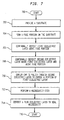
- Fig. 7 illustrates, in accordance with one embodiment of the present invention, the steps employed in the formation of a typical electrically blowable fuse.
- a substrate is provided.
- the substrate may represent a silicon substrate on which devices have already been formed.
- a fuse portion e.g., a conductor formed of a fuse material, is formed.
- the first and second dielectric layers are conformally deposited.
- a CMP step is employed to polish through the second dielectric layer at the protruded spot to expose a portion of the underlying first dielectric layer.
- a microcavity etch step is employed to etch a microcavity in the first dielectric layer through the opening in the hard mask/second dielectric layer while leaving the hard mask and the fuse portion substantially unetched.
- a third dielectric layer representing a plug layer is deposited to close up the opening in the hard mask/second dielectric layer, thereby sealing the microcavity from the outside.
- the photolithography step employed in the prior art to form a hard mask out of second dielectric layer 304 has been eliminated. Accordingly, the high cost and alignment problems associated with the photolithography step are also advantageously eliminated.
- the present invention employs chemical mechanical polish (CMP) as a mask forming technique.
- CMP chemical mechanical polish
- the use of CMP as a mask forming technique is nonobvious since CMP is typically regarded as a planarizing step, i.e., not as a step to form selective, aligned openings in a layer.
- CMP CMP
- CMP material removal depth tends to be difficult to control and scratches may form on the substrate if the CMP process is not carefully designed.
- the use of a CMP step is also nonobvious since CMP tends to generate particulate matter (in the form of a slurry), which requires subsequent cleaning steps and is therefore generally undesired by process engineers.
- most fabrication facilities do not have CMP tools. Accordingly, most process engineers would not naturally think of CMP as a process to create a hard mask.
- the invention takes advantage of the intrinsic nature of the CMP process to attack high spots or protrusions on the substrate surface to automatically align the opening of the hard mask with the underlying fuse portion. Because of this, microcavity 502 is correctly positioned about fuse portion 102 in a subsequent microcavity etch step.
- the CMP step may be performed using a soft pad, i.e., a pad that can locally "adapt" to the underlying topography to ensure that the CMP step removes only the protrusions or high spots above the fuse portions without inadvertently removing the dielectric material from other raised portions of the integrated circuit.
- a soft pad i.e., a pad that can locally "adapt" to the underlying topography to ensure that the CMP step removes only the protrusions or high spots above the fuse portions without inadvertently removing the dielectric material from other raised portions of the integrated circuit.
- supplemental design rules may be specified to prevent the inadvertent removal of the dielectric material from other raised portions of the integrated circuit.
- the electrically blowable fuses may be positioned away from other structures of the IC.
- dummy structures may be put around structures which need to be protected from CMP. These additional dummy structures form raised plateaus instead of isolated raised protrusions or high spots, which tend to be more readily attacked by the
Landscapes
- Design And Manufacture Of Integrated Circuits (AREA)
- Semiconductor Memories (AREA)
- Semiconductor Integrated Circuits (AREA)
Description
- The present invention relates to the fabrication of semiconductor devices. More particularly, the present invention relates to improved techniques for fabricating electrically blowable fuses on a semiconductor substrate.
- Fuses have long been employed in integrated circuits. A fuse typically comprises a fuse portion formed of a fuse material that may be turned into a non-conductive state through various mechanisms. When the fuse is in its conductive state, an electrical current may pass through the fuse portion. When the fuse is blown, i.e., becomes non-conductive, an open circuit is created through which very little, if any, current may pass.
- Exemplary uses of fuses include, for example, protecting sensitive portions of the integrated circuit during manufacturing to prevent a build up of charge from damaging the sensitive electronic devices thereon. After the integrated circuit is manufactured, the fuse may be blown to sever the current path, and the resulting IC may be employed as if the current path never existed. Fuses may also be employed to, for example, set the address bits of a redundant element in a dynamic random access memory (DRAM) array in order to specify to the decoding circuit the address of the defective main memory array element. With the address information furnished by the fuses, the redundant element may then be employed to replace the defective main memory array element.
- Although there are many fuse designs today, two types of fuses have received wide acceptance: laser blowable fuses and electrically blowable fuses. With laser blowable fuses, the fuses are typically formed at or near the surface of the integrated circuit. A laser beam striking the fuse material renders the fuse portion non-conductive, thereby inhibiting current from flowing through. Although laser blowable fuses are relatively simple to fabricate, there are disadvantages. For example, the laser blowable fuses tend to be surface oriented, which places a limitation on the design of the IC. Further, laser blowable fuses tend to occupy a large amount of space on the IC surface since the adjacent fuses or devices must not be placed too close to the fuse or risk being inadvertently damaged by the laser beam during the fuse setting operation.
- Electrically blowable fuses, on the other hand, do not have to be placed at or near the surface of the integrated circuit. Accordingly, they give the designers greater latitude in fuse placement. In general, they tend to be smaller than laser blowable fuses, which render them highly suitable for use in modern high density integrated circuits.
- In a typically electrically blowable fuse, the fuse portion, typically formed of a material that changes its state from conductive to non-conductive when a current exceeding a predefined threshold is passed through, is typically disposed in a dielectric microcavity, i.e., a sealed, hollow chamber in a dielectric layer. The microcavity itself is typically formed in a multistep process, which conventionally requires one or more photolithography steps in the prior art.
- To facilitate discussion, Figs. 1 and 2 illustrate the prior art process for forming an electrically blowable fuse. Referring initially to Fig. 1, a
fuse portion 102 is shown disposed on asubstrate 104.Fuse portion 102 typically comprises a conductor made of a suitable fuse material such as doped polysilicon or metal. For reasons which will become apparent shortly, the fuse portion is typically capped with a silicon nitride layer. - As mentioned,
fuse portion 102 is dimensioned and configured such that when a current exceeding a predefined current value passes throughfuse portion 102, it changes to a non-conductive state to essentially inhibit current from subsequently flowing through.Substrate 104 typically represents an oxide layer and may include any other structures of the integrated circuit. By way of example and not by way of limitation,substrate 104 may represent a gate oxide or even any oxide layer above a shallow trench isolation (STI) area. Abovefuse portion 102, anotheroxide layer 106 is conformally deposited. Asilicon nitride layer 108 is then deposited aboveoxide layer 106. - Above
silicon nitride layer 108, aphotoresist layer 110 is deposited and patterned to form anopening 112. Patternedphotoresist mask 110 is then employed to etch throughsilicon nitride layer 108 to expose a portion ofoxide layer 106 abovefuse portion 102. After an opening insilicon nitride layer 108 is formed, a subsequent isotropic etch is performed to create the microcavity. As is apparent,silicon nitride layer 108 acts as a hard mask during the isotropic etch ofmicrocavity 202. - In Fig. 2,
microcavity 202 has been isotropically etched out ofoxide layer 106 through the opening insilicon nitride layer 108. The microcavity etch preferably employs an etch process that is selective both to the liner material offuse portion 102 andsilicon nitride layer 108. - Subsequent to the formation of
microcavity 202, aplug layer 206, e.g., another oxide layer, is then deposited. The deposition process that formsplug layer 206 is such that the opening in the silicon nitride layer is sealed with the plug material whilemicrocavity 202 is left hollow. Thusfuse portion 102 is essentially sealed withinmicrocavity 202 after the deposition ofplug layer 206. Accordingly, any particulate material that may be formed whenfuse portion 102 is blown is kept contained withinmicrocavity 202, thereby minimizing or essentially eliminating any possibility of particulate contamination of the IC surface. - It has been found, however, that the conventional process of forming electrically
blowable fuse 100 has some disadvantages. In particular, the prior art technique of forming electrically blowable fuses requires at least one photolithography step to pattern a hard mask out ofsilicon nitride layer 108. As is known by those skilled in the art, photolithography is an expensive process and is therefore generally undesirable from a cost standpoint. Further, as the density of the integrated circuit increases and its feature sizes decrease, accurate alignment becomes problematic. By way of example, asfuse portion 102 decreases in width and the adjacent fuses and/or devices are packed closer together, the accurate alignment of opening 112 inphotoresist layer 110 withfuse portion 102 becomes increasingly difficult. These and other challenges presented by the photolithography step render the fabrication of electricallyblowable fuses 100 unduly expensive and, in many cases, even prohibitively expensive. - In view of the foregoing, there are desired improved techniques for fabricating electrically blowable fuses. In particular, there are desired improved techniques for forming electrically blowable fuses that do not require the use of a photolithography step to form a hard mask for the subsequent microcavity etch.
- Patent abstract of Japan 01-295439 discloses forming a cavity at least at the upper part or the lower part of a narrow region which is provided as a part of a wiring layer of a fuse.
- US 4,675,984 discloses a method of exposing only the top surface of a narrow mesa wherein a protective layer may be very precisely formed on a very narrow mesa for subsequent doping of areas adjacent the mesa without doping the mesa itself. A variation of the invention includes forming an opening directly over the narrow mesa so that a contact may be made at only the top surface of the mesa or the upper portion of the mesa may be doped independent of surfaces adjacent the mesa.
- The invention relates to a method for fabricating an electrically blowable fuse on a semiconductor substrate. The method includes forming a fuse portion on the semiconductor substrate. The fuse portion is configured to turn substantially non-conductive when a current exceeding a predefined current level passes through the fuse portion. The method also includes depositing a substantially conformal first layer of dielectric material above the fuse portion and depositing a second layer of dielectric material above the first layer, said first layer and said second layer thereby forming a protrusion of dielectric material above the fuse portion. The second layer comprises a material that said first layer can be etched selectively thereto.
- The method further includes performing chemical-mechanical polish on the protrusion to form an opening through the second layer. There is also included etching, in a substantially isotropic manner, a portion of the first layer through the opening to form a microcavity about the fuse portion. The etching is substantially selective to the second layer and the fuse portion. Additionally, there is included depositing a substantially conformal third layer of dielectric material above the second layer, thereby closing the opening in the second layer.
- In one embodiment, the invention relates to a method as described above wherein said second layer of dielectric material is conformally deposited above said first layer.
- These and other features of the present invention will be described in more detail below in the detailed description of the invention and in conjunction with the following figures.
- The present invention is illustrated by way of example, and not by way of limitation, in the figures of the accompanying drawings and in which like reference numerals refer to similar elements and in which:
- Figs. 1 and 2 illustrate, to facilitate discussion, the conventional prior art technique for forming an electrically blowable fuse on an IC.
- Figs. 3, 4, 5, and 6 illustrate, in accordance with one aspect of the present invention, the improved technique for forming an electrically blowable fuse on an IC.
- Fig. 7 illustrate, in accordance with one aspect of the present invention, the steps for forming the electrically blowable fuse of Fig. 6.
- The present invention will now be described in detail with reference to a few embodiments thereof as illustrated in the accompanying drawings. In the following description, numerous specific details are set forth in order to provide a thorough understanding of the present invention. It will be apparent, however, to one skilled in the art, that the present invention may be practiced without some or all of these specific details. In other instances well known process steps and/or structures have not been described in detail in order to not unnecessarily obscure the present invention.
- In one embodiment, there are provided techniques for forming electrically blowable fuses used in an ICs. Such IC includes a random access memory (RAM), a dynamic random access memory (DRAM), a synchronous DRAM (SDRAM), and a read only memory (ROM). Other types of ICs include application specific integrated circuits (ASICs) or any logic circuit. Typically, a plurality of ICs are formed on the wafer in parallel. After processing is finish, the wafer is diced to separate the ICs to individual chips. The chips are then packaged, resulting in a final product that is used in, for example, consumer products such as computer systems, cellular phones, personal digital assistants (PDAs), and other electronic products. The electrically blowable fuses are formed without requiring the use of a photolithography step to create a hard mask for the subsequent microcavity etch. In one embodiment, the opening in the hard mask is achieved by abrading or polishing through the hard mask layer using a relatively short chemical-mechanical polish (CMP) step.
- The invention takes advantage of the intrinsic tendency of the CMP process for attacking isolated high spots on the substrate surface to solve the alignment problem i.e., the alignment of the hard mask opening with the underlying fuse portion. It is advantageously recognized that since the high spots or protrusions are formed above the fuse portion through the use of conformal dielectric layer deposition, the CMP process automatically aligns the abraded spot, i.e., the opening in the vicinity of the high spot, with the underlying fuse portion. Once the opening is created, a subsequent microcavity etch may be employed to create the microcavity for the fuse.
- The features and advantages of the invention may be better understood with reference to the Figures that follow. Figs. 3, 4, 5, and 6 illustrate, in accordance with one aspect of the present invention, the improved technique for forming electrically blowable fuses. As in Figs. 1 and 2, a
fuse portion 102 is again shown disposed abovesubstrate 104 in Fig. 3. As mentioned earlier,fuse portion 102 preferably comprises a conductor formed of an appropriate fuse material such as polysilicon or metal. Polysilicon is preferred, in some applications, as the fuse material since it may offer a greater thermal budget. In one embodiment,fuse portion 102 may be employed to protect the gate structures of transistors and may therefore be formed from the same layers that are used to form the gates of transistors. In some of these applications a layer of tungsten silicide or titanium silicide may cover the layer of fuse material. A silicon nitride liner may be provided to encapsulate and protectfuse portion 102 from being attacked in the subsequent microcavity etch. In one exemplary application, the fuse structure may be about 500 - 600 nanometers (5,000 - 6,000 angstroms) thick. - Above
fuse portion 102 andsubstrate 104, a firstdielectric layer 302 is conformally deposited. In one exemplary application, firstdielectric layer 302 may be about 800-900 nanometers (8,000 - 9,000 angstroms) thick. Firstdielectric layer 302 may be formed of any suitable dielectric material that may be conformally deposited overfuse portion 102 andsubstrate 104. In one embodiment, firstdielectric layer 302 represents a layer of boro-phosphosilicate (BPSG) glass. Firstdielectric layer 302 may also be a layer of phosphorous doped silicate glass (PSG) or phosphorous doped high density oxide (PHDP-oxide). Firstdielectric layer 302 may in fact be any doped oxide layer or any type of suitable conformal dielectric material. In one particularly advantageous embodiment, the first dielectric layer represents a layer of glass deposited by a conventional high density plasma process. As the term is employed herein, high density plasma deposition refers to the deposition of materials in a low pressure plasma CVD chamber that employs not only a source but also bias power to permit simultaneous deposition and sputtering. The high density plasma film conformally coversfuse portion 102 while substantially planarizing smaller, more tightly spaced features on the IC. - Above
first dielectric layer 302, asecond dielectric layer 304 is deposited. The thickness of the second dielectric layer is sufficient to serve as an etch mask for the subsequent etch that forms a microcavity withinfirst dielectric layer 302. The thickness of thesecond dielectric layer 304 may be about 100 nanometers (1,000 angstroms). Thesecond dielectric layer 304 comprises a material that the first dielectric layer can be etched selectively thereto. That is, the etch effectively removes the first dielectric layer without removing the second dielectric layer. In one embodiment, thesecond dielectric layer 304 comprises silicon nitride. Other suitable dielectric material which the first dielectric layer can be etched selectively thereto may also be employed. - Illustratively, the second dielectric layer is conformally deposited over the first dielectric layer. As such, the topography of the underlying layer is reflected in the deposited layer, resulting in a protrusion on the surface of the substrate. Because of the underlying fuse portion, the protrusion is formed directly above fused
portion 102, as shown in Fig. 3. A non-conformally deposited second dielectric layer is also useful. When a non-conformal layer is deposited, the topography of the underlying layer is not reflected therein. - In Fig. 4, a chemical mechanical polish (CMP) step is employed to polish or abrade the protrusion above
fuse portion 102 to break through seconddielectric layer 304 and expose a portion of firstdielectric layer 302 to the subsequent microcavity etch. The opening in seconddielectric layer 304 is shown in Fig. 4 asopening 408. The invention employs, in one embodiment, thefirst dielectric layer 302 as a CMP stop layer. In other words, the CMP process stops as soon as or shortly after the underlying firstdielectric layer 302 is exposed. In general the CMP step may be relatively short, which tends to improve throughput, e.g. about 10-60 seconds in some cases. As can be appreciated by those skilled in the art, the CMP step is employed, in a nonobvious manner, in the formation of the hard mask that is employed to subsequently etch the microcavity in thefirst dielectric layer 302. In embodiments employing a non-conformal second dielectric layer, the CMP time may be increased since more material may need to be removed before - exposing the underlying first dielectric layer. - In Fig. 5, a microcavity has been etched in first
dielectric layer 302 throughopening 408 in hard mask/second dielectric layer 304. The microcavity etch step is preferably designed such that it does not unduly attack seconddielectric layer 304 andfuse portion 102. As seconddielectric layer 304 and the protective liner encapsulatingfuse portion 102 are made of a silicon nitride material in one embodiment, the microcavity etch preferably employs an etchant that does not unduly attack silicon nitride. In one embodiment, an wet (e.g., isotropic) HF etch works well for a BPSG firstdielectric layer 302. However, isotropic etching is not a requirement and etching may be performed in a somewhat anisotropic manner as long as such etching results in a microcavity that is capable of being subsequently sealed. - In Fig. 6, a third
dielectric layer 606 is deposited above seconddielectric layer 304.Third dielectric layer 606 may, for example, represent a low pressure chemical vapor deposition oxide layer (LPCVD) or LPCVD TEOS.Third dielectric layer 606 represents a plug dielectric layer, whose deposition process is configured to sealopening 408 in seconddielectric layer 304 without fillingmicrocavity 502 with dielectric material, thereby sealingmicrocavity 502 from the rest of the integrated circuit. Whenfuse portion 102 is blown, any particulate material that is generated is advantageously kept withinmicrocavity 502, thereby minimizing or substantially eliminating particulate contamination problems during the fuse setting process. - Fig. 7 illustrates, in accordance with one embodiment of the present invention, the steps employed in the formation of a typical electrically blowable fuse. In
step 702, a substrate is provided. As mentioned, the substrate may represent a silicon substrate on which devices have already been formed. Instep 704, a fuse portion, e.g., a conductor formed of a fuse material, is formed. Insteps step 710, a CMP step is employed to polish through the second dielectric layer at the protruded spot to expose a portion of the underlying first dielectric layer. In -step 712, a microcavity etch step is employed to etch a microcavity in the first dielectric layer through the opening in the hard mask/second dielectric layer while leaving the hard mask and the fuse portion substantially unetched. Instep 714, a third dielectric layer representing a plug layer is deposited to close up the opening in the hard mask/second dielectric layer, thereby sealing the microcavity from the outside. - As can be appreciated from the foregoing, the photolithography step employed in the prior art to form a hard mask out of second
dielectric layer 304 has been eliminated. Accordingly, the high cost and alignment problems associated with the photolithography step are also advantageously eliminated. In a nonobvious manner, the present invention employs chemical mechanical polish (CMP) as a mask forming technique. The use of CMP as a mask forming technique is nonobvious since CMP is typically regarded as a planarizing step, i.e., not as a step to form selective, aligned openings in a layer. Further, it would be nonobvious to employ CMP to form a hard mask since CMP is generally not favored by process engineers since the CMP material removal depth tends to be difficult to control and scratches may form on the substrate if the CMP process is not carefully designed. The use of a CMP step is also nonobvious since CMP tends to generate particulate matter (in the form of a slurry), which requires subsequent cleaning steps and is therefore generally undesired by process engineers. Further, most fabrication facilities do not have CMP tools. Accordingly, most process engineers would not naturally think of CMP as a process to create a hard mask. - Further, the invention takes advantage of the intrinsic nature of the CMP process to attack high spots or protrusions on the substrate surface to automatically align the opening of the hard mask with the underlying fuse portion. Because of this,
microcavity 502 is correctly positioned aboutfuse portion 102 in a subsequent microcavity etch step. - In accordance with another aspect of the present invention, the CMP step may be performed using a soft pad, i.e., a pad that can locally "adapt" to the underlying topography to ensure that the CMP step removes only the protrusions or high spots above the fuse portions without inadvertently removing the dielectric material from other raised portions of the integrated circuit. Alternatively or additionally, supplemental design rules may be specified to prevent the inadvertent removal of the dielectric material from other raised portions of the integrated circuit. To ensure protection of raised areas where CMP removal is not desired, the electrically blowable fuses may be positioned away from other structures of the IC. Alternatively or additionally, dummy structures may be put around structures which need to be protected from CMP. These additional dummy structures form raised plateaus instead of isolated raised protrusions or high spots, which tend to be more readily attacked by the CMP process.
- While this invention has been described in terms of several preferred embodiments, there are alterations, permutations, and equivalents which fall within the scope of this invention. By way of example, although the disclosures refers mainly to DRAMS, the fuses formed in accordance with the techniques disclosed herein may be employed in any fuse application on any type of IC, e.g., to protect sensitive components and/or provide binary values.
Claims (12)
- A method for fabricating an electrically blowable fuse on a semiconductor substrate (104), comprising:forming a fuse portion (102) on said semiconductor substrate (104), said fuse portion (102) being configured to turn substantially non-conductive when a current exceeding a predefined current level passes through said fuse portion (102);depositing a substantially conformal first layer (302) of dielectric material above said fuse portion (102);depositing a second layer (304) of dielectric material above said first layer (302), said second layer (304) comprising a material that said first layer (302) can be etched selectively thereto, said first layer (302) and said second layer (304) thereby forming a protrusion of dielectric material above said fuse portion (102);performing chemical-mechanical polish on said protrusion to form an opening (408) through said second layer (304);etching, in a substantially isotropic manner, a portion of said first layer through said opening (408) to form a microcavity about said fuse portion (102), said etching being substantially selective to said second layer (304) and said fuse portion (102); anddepositing a substantially conformal third layer (606) of dielectric material above said second layer (304), thereby closing said opening (408) in said second layer (304).
- The method of claim 1 wherein said fuse portion (102) includes a polysilicon conductor.
- The method of claim 1 wherein said fuse portion (102) includes a metallic conductor.
- The method of claim 1 wherein said first layer (302) represents a silicon oxide layer and said second layer (304) represents a silicon nitride layer.
- The method of claim 1 wherein said first layer (302) represents a doped oxide layer, said second layer (304) represents a silicon nitride layer.
- The method of claim 1 wherein said first layer (302) represents a phosphorous doped silicate glass (PSG) layer, said second layer (304) represents a silicon nitride layer.
- The method of claim 1 wherein said first layer (302) represents a boro-phosphosilicate glass (BPSG) layer, said second layer (304) represents a silicon nitride layer.
- The method of claim 7 wherein said first layer (302) is deposited by a high density plasma chemical vapor deposition process.
- The method of claim 8 wherein said performing chemical-mechanical polish employs a soft pad.
- The method of claim 1 wherein said fuse portion (102) includes a polysilicon conductor covered with a silicon nitride liner.
- The method of claim 1 wherein said semiconductor substrate (104) represents a substrate employed to manufacture dynamic random access memory (DRAM) circuits.
- The method of claim 1, wherein said second layer (304) of dielectric material is conformally deposited above said first layer (302).
Applications Claiming Priority (2)
| Application Number | Priority Date | Filing Date | Title |
|---|---|---|---|
| US933955 | 1997-09-19 | ||
| US08/933,955 US5899736A (en) | 1997-09-19 | 1997-09-19 | Techniques for forming electrically blowable fuses on an integrated circuit |
Publications (3)
| Publication Number | Publication Date |
|---|---|
| EP0903784A2 EP0903784A2 (en) | 1999-03-24 |
| EP0903784A3 EP0903784A3 (en) | 2005-03-23 |
| EP0903784B1 true EP0903784B1 (en) | 2007-04-18 |
Family
ID=25464717
Family Applications (1)
| Application Number | Title | Priority Date | Filing Date |
|---|---|---|---|
| EP98112434A Expired - Lifetime EP0903784B1 (en) | 1997-09-19 | 1998-07-04 | Improved techniques for forming electrically blowable fuses on an integrated circuit |
Country Status (7)
| Country | Link |
|---|---|
| US (1) | US5899736A (en) |
| EP (1) | EP0903784B1 (en) |
| JP (1) | JPH11150190A (en) |
| KR (1) | KR100538911B1 (en) |
| CN (1) | CN1129187C (en) |
| DE (1) | DE69837585T2 (en) |
| TW (1) | TW437046B (en) |
Cited By (1)
| Publication number | Priority date | Publication date | Assignee | Title |
|---|---|---|---|---|
| US7849477B2 (en) | 2007-01-30 | 2010-12-07 | Invidi Technologies Corporation | Asset targeting system for limited resource environments |
Families Citing this family (15)
| Publication number | Priority date | Publication date | Assignee | Title |
|---|---|---|---|---|
| US6060398A (en) * | 1998-03-09 | 2000-05-09 | Siemens Aktiengesellschaft | Guard cell for etching |
| US6268638B1 (en) * | 1999-02-26 | 2001-07-31 | International Business Machines Corporation | Metal wire fuse structure with cavity |
| US6274440B1 (en) * | 1999-03-31 | 2001-08-14 | International Business Machines Corporation | Manufacturing of cavity fuses on gate conductor level |
| DE19926107C1 (en) | 1999-06-08 | 2000-11-16 | Siemens Ag | Semiconductor structure, especially a memory including redundant memory cells or word lines, has a vertical fuse embedded in a cavity of a semiconductor body |
| US6166421A (en) * | 1999-08-18 | 2000-12-26 | National Semiconductor Corporation | Polysilicon fuse that provides an open current path when programmed without exposing the fuse to the environment |
| US6210995B1 (en) * | 1999-09-09 | 2001-04-03 | International Business Machines Corporation | Method for manufacturing fusible links in a semiconductor device |
| US6500771B1 (en) | 2000-01-31 | 2002-12-31 | Chartered Semiconductor Manufacturing Ltd. | Method of high-density plasma boron-containing silicate glass film deposition |
| US6368902B1 (en) | 2000-05-30 | 2002-04-09 | International Business Machines Corporation | Enhanced efuses by the local degradation of the fuse link |
| US6495901B2 (en) | 2001-01-30 | 2002-12-17 | Infineon Technologies Ag | Multi-level fuse structure |
| US7541240B2 (en) * | 2005-10-18 | 2009-06-02 | Sandisk Corporation | Integration process flow for flash devices with low gap fill aspect ratio |
| US7576407B2 (en) * | 2006-04-26 | 2009-08-18 | Samsung Electronics Co., Ltd. | Devices and methods for constructing electrically programmable integrated fuses for low power applications |
| US7825490B2 (en) * | 2007-07-18 | 2010-11-02 | International Business Machines Corporation | Electrical fuse having a cavity thereupon |
| CN103094250B (en) * | 2012-12-25 | 2015-12-23 | 杭州士兰集成电路有限公司 | One trims resistance and manufacture method thereof |
| US9455222B1 (en) * | 2015-12-18 | 2016-09-27 | Texas Instruments Incorporated | IC having failsafe fuse on field dielectric |
| CN114103095A (en) * | 2021-11-22 | 2022-03-01 | 航天特种材料及工艺技术研究所 | Lightweight aircraft based on lattice structure material and manufacturing method thereof |
Family Cites Families (9)
| Publication number | Priority date | Publication date | Assignee | Title |
|---|---|---|---|---|
| JPS60134437A (en) * | 1983-12-23 | 1985-07-17 | Nippon Telegr & Teleph Corp <Ntt> | Fusing device and manufacture thereof |
| US4675984A (en) * | 1985-09-19 | 1987-06-30 | Rca Corporation | Method of exposing only the top surface of a mesa |
| JPH01295439A (en) * | 1988-05-24 | 1989-11-29 | Nissan Motor Co Ltd | Semiconductor device |
| JP2665568B2 (en) * | 1990-11-21 | 1997-10-22 | シャープ株式会社 | Method for manufacturing semiconductor device |
| US5675174A (en) * | 1993-01-06 | 1997-10-07 | Rohm Co., Ltd. | Method for using fuse structure in semiconductor device |
| US5729042A (en) * | 1995-08-14 | 1998-03-17 | Vanguard International Semiconductor Corporation | Raised fuse structure for laser repair |
| KR970013224A (en) * | 1995-08-28 | 1997-03-29 | 김광호 | Semiconductor device having laser fuse and manufacturing method thereof |
| DE19638666C1 (en) * | 1996-01-08 | 1997-11-20 | Siemens Ag | Fuse with a protective layer in an integrated semiconductor circuit and associated manufacturing process |
| KR100218685B1 (en) * | 1996-09-02 | 1999-09-01 | 정선종 | Manufacturing method of field emission device |
-
1997
- 1997-09-19 US US08/933,955 patent/US5899736A/en not_active Expired - Fee Related
-
1998
- 1998-07-04 EP EP98112434A patent/EP0903784B1/en not_active Expired - Lifetime
- 1998-07-04 DE DE69837585T patent/DE69837585T2/en not_active Expired - Lifetime
- 1998-08-06 TW TW087112966A patent/TW437046B/en not_active IP Right Cessation
- 1998-08-25 CN CN98118680A patent/CN1129187C/en not_active Expired - Fee Related
- 1998-09-10 KR KR1019980037262A patent/KR100538911B1/en not_active Expired - Fee Related
- 1998-09-17 JP JP10263009A patent/JPH11150190A/en not_active Withdrawn
Non-Patent Citations (1)
| Title |
|---|
| None * |
Cited By (1)
| Publication number | Priority date | Publication date | Assignee | Title |
|---|---|---|---|---|
| US7849477B2 (en) | 2007-01-30 | 2010-12-07 | Invidi Technologies Corporation | Asset targeting system for limited resource environments |
Also Published As
| Publication number | Publication date |
|---|---|
| DE69837585T2 (en) | 2008-01-03 |
| EP0903784A3 (en) | 2005-03-23 |
| KR100538911B1 (en) | 2006-03-20 |
| CN1212457A (en) | 1999-03-31 |
| DE69837585D1 (en) | 2007-05-31 |
| CN1129187C (en) | 2003-11-26 |
| US5899736A (en) | 1999-05-04 |
| TW437046B (en) | 2001-05-28 |
| EP0903784A2 (en) | 1999-03-24 |
| JPH11150190A (en) | 1999-06-02 |
| KR19990029669A (en) | 1999-04-26 |
Similar Documents
| Publication | Publication Date | Title |
|---|---|---|
| EP0903784B1 (en) | Improved techniques for forming electrically blowable fuses on an integrated circuit | |
| JP4907838B2 (en) | Memory device having a recessed gate structure | |
| US6027998A (en) | Method for fully planarized conductive line for a stack gate | |
| US6124165A (en) | Method for making openings in a passivation layer over polycide fuses using a single mask while forming reliable tungsten via plugs on DRAMs | |
| US9263384B2 (en) | Programmable devices and methods of manufacture thereof | |
| EP0967638B1 (en) | Semiconductor fuse | |
| USRE40339E1 (en) | Silicon-on-insulator chip having an isolation barrier for reliability | |
| US6046503A (en) | Metalization system having an enhanced thermal conductivity | |
| US6808975B2 (en) | Method for forming a self-aligned contact hole in a semiconductor device | |
| KR19990063531A (en) | How to reduce pad corrosion | |
| JP3902507B2 (en) | Repair fuse opening method of semiconductor element | |
| KR100504262B1 (en) | Reduction of pad erosion | |
| US6797611B1 (en) | Method of fabricating contact holes on a semiconductor chip | |
| EP0942462B1 (en) | Method and structure for protecting a neighbouring area adjacent to an area to be etched and method for forming a fuse | |
| US6724054B1 (en) | Self-aligned contact formation using double SiN spacers | |
| HK1016748A (en) | Improved techniques for forming electrically blowable fuses on an integrated circuit | |
| US6432827B1 (en) | ILD planarization method | |
| EP0942461A2 (en) | Reduction of black silicon in semiconductor fabrication | |
| KR19990030133A (en) | Multi-level conductive structure and method of manufacturing the same | |
| US6617233B2 (en) | Process of fabricating an anti-fuse for avoiding a key hole exposed | |
| KR100388206B1 (en) | Method for manufacturing capacitor of semiconductor device | |
| US6093650A (en) | Method for fully planarized conductive line for a stack gate | |
| HK1019512A (en) | Method and structure for protecting a neighbouring area adjacent to an area to be etched and method for forming a fuse | |
| KR20010059986A (en) | Method for forming fuse box | |
| HK1022045A (en) | Semiconductor fuse |
Legal Events
| Date | Code | Title | Description |
|---|---|---|---|
| PUAI | Public reference made under article 153(3) epc to a published international application that has entered the european phase |
Free format text: ORIGINAL CODE: 0009012 |
|
| AK | Designated contracting states |
Kind code of ref document: A2 Designated state(s): AT BE CH CY DE DK ES FI FR GB GR IE IT LI LU MC NL PT SE |
|
| AX | Request for extension of the european patent |
Free format text: AL;LT;LV;MK;RO;SI |
|
| PUAL | Search report despatched |
Free format text: ORIGINAL CODE: 0009013 |
|
| AK | Designated contracting states |
Kind code of ref document: A3 Designated state(s): AT BE CH CY DE DK ES FI FR GB GR IE IT LI LU MC NL PT SE |
|
| AX | Request for extension of the european patent |
Extension state: AL LT LV MK RO SI |
|
| 17P | Request for examination filed |
Effective date: 20050420 |
|
| AKX | Designation fees paid |
Designated state(s): DE FR GB IE IT NL |
|
| REG | Reference to a national code |
Ref country code: HK Ref legal event code: WD Ref document number: 1016748 Country of ref document: HK |
|
| 17Q | First examination report despatched |
Effective date: 20060217 |
|
| GRAP | Despatch of communication of intention to grant a patent |
Free format text: ORIGINAL CODE: EPIDOSNIGR1 |
|
| GRAS | Grant fee paid |
Free format text: ORIGINAL CODE: EPIDOSNIGR3 |
|
| GRAA | (expected) grant |
Free format text: ORIGINAL CODE: 0009210 |
|
| AK | Designated contracting states |
Kind code of ref document: B1 Designated state(s): DE FR GB IE IT NL |
|
| REG | Reference to a national code |
Ref country code: IE Ref legal event code: FG4D |
|
| REF | Corresponds to: |
Ref document number: 69837585 Country of ref document: DE Date of ref document: 20070531 Kind code of ref document: P |
|
| RAP2 | Party data changed (patent owner data changed or rights of a patent transferred) |
Owner name: QIMONDA AG |
|
| NLT2 | Nl: modifications (of names), taken from the european patent patent bulletin |
Owner name: QIMONDA AG Effective date: 20070711 |
|
| NLV1 | Nl: lapsed or annulled due to failure to fulfill the requirements of art. 29p and 29m of the patents act | ||
| EN | Fr: translation not filed | ||
| PG25 | Lapsed in a contracting state [announced via postgrant information from national office to epo] |
Ref country code: NL Free format text: LAPSE BECAUSE OF FAILURE TO SUBMIT A TRANSLATION OF THE DESCRIPTION OR TO PAY THE FEE WITHIN THE PRESCRIBED TIME-LIMIT Effective date: 20070418 |
|
| PLBE | No opposition filed within time limit |
Free format text: ORIGINAL CODE: 0009261 |
|
| STAA | Information on the status of an ep patent application or granted ep patent |
Free format text: STATUS: NO OPPOSITION FILED WITHIN TIME LIMIT |
|
| 26N | No opposition filed |
Effective date: 20080121 |
|
| GBPC | Gb: european patent ceased through non-payment of renewal fee |
Effective date: 20070718 |
|
| PG25 | Lapsed in a contracting state [announced via postgrant information from national office to epo] |
Ref country code: IT Free format text: LAPSE BECAUSE OF FAILURE TO SUBMIT A TRANSLATION OF THE DESCRIPTION OR TO PAY THE FEE WITHIN THE PRESCRIBED TIME-LIMIT Effective date: 20070418 Ref country code: FR Free format text: LAPSE BECAUSE OF FAILURE TO SUBMIT A TRANSLATION OF THE DESCRIPTION OR TO PAY THE FEE WITHIN THE PRESCRIBED TIME-LIMIT Effective date: 20071214 |
|
| PG25 | Lapsed in a contracting state [announced via postgrant information from national office to epo] |
Ref country code: GB Free format text: LAPSE BECAUSE OF NON-PAYMENT OF DUE FEES Effective date: 20070718 |
|
| PG25 | Lapsed in a contracting state [announced via postgrant information from national office to epo] |
Ref country code: IE Free format text: LAPSE BECAUSE OF NON-PAYMENT OF DUE FEES Effective date: 20070704 |
|
| PG25 | Lapsed in a contracting state [announced via postgrant information from national office to epo] |
Ref country code: FR Free format text: LAPSE BECAUSE OF FAILURE TO SUBMIT A TRANSLATION OF THE DESCRIPTION OR TO PAY THE FEE WITHIN THE PRESCRIBED TIME-LIMIT Effective date: 20070418 |
|
| REG | Reference to a national code |
Ref country code: DE Ref legal event code: R081 Ref document number: 69837585 Country of ref document: DE Owner name: POLARIS INNOVATIONS LTD., IE Free format text: FORMER OWNER: QIMONDA AG, 81739 MUENCHEN, DE Ref country code: DE Ref legal event code: R081 Ref document number: 69837585 Country of ref document: DE Owner name: INFINEON TECHNOLOGIES AG, DE Free format text: FORMER OWNER: QIMONDA AG, 81739 MUENCHEN, DE |
|
| REG | Reference to a national code |
Ref country code: DE Ref legal event code: R081 Ref document number: 69837585 Country of ref document: DE Owner name: POLARIS INNOVATIONS LTD., IE Free format text: FORMER OWNER: INFINEON TECHNOLOGIES AG, 85579 NEUBIBERG, DE |
|
| PGFP | Annual fee paid to national office [announced via postgrant information from national office to epo] |
Ref country code: DE Payment date: 20160628 Year of fee payment: 19 |
|
| REG | Reference to a national code |
Ref country code: DE Ref legal event code: R119 Ref document number: 69837585 Country of ref document: DE |
|
| PG25 | Lapsed in a contracting state [announced via postgrant information from national office to epo] |
Ref country code: DE Free format text: LAPSE BECAUSE OF NON-PAYMENT OF DUE FEES Effective date: 20180201 |