EP0903669B1 - Procédé et dispositif de commande de mémoire appropriés pour un système de traitement d'information - Google Patents
Procédé et dispositif de commande de mémoire appropriés pour un système de traitement d'information Download PDFInfo
- Publication number
- EP0903669B1 EP0903669B1 EP98122596A EP98122596A EP0903669B1 EP 0903669 B1 EP0903669 B1 EP 0903669B1 EP 98122596 A EP98122596 A EP 98122596A EP 98122596 A EP98122596 A EP 98122596A EP 0903669 B1 EP0903669 B1 EP 0903669B1
- Authority
- EP
- European Patent Office
- Prior art keywords
- unit
- memory
- request
- checking
- control unit
- Prior art date
- Legal status (The legal status is an assumption and is not a legal conclusion. Google has not performed a legal analysis and makes no representation as to the accuracy of the status listed.)
- Expired - Lifetime
Links
Images


Classifications
-
- G—PHYSICS
- G06—COMPUTING OR CALCULATING; COUNTING
- G06F—ELECTRIC DIGITAL DATA PROCESSING
- G06F12/00—Accessing, addressing or allocating within memory systems or architectures
- G06F12/02—Addressing or allocation; Relocation
- G06F12/08—Addressing or allocation; Relocation in hierarchically structured memory systems, e.g. virtual memory systems
- G06F12/0802—Addressing of a memory level in which the access to the desired data or data block requires associative addressing means, e.g. caches
- G06F12/0806—Multiuser, multiprocessor or multiprocessing cache systems
- G06F12/0815—Cache consistency protocols
- G06F12/0817—Cache consistency protocols using directory methods
- G06F12/0822—Copy directories
-
- G—PHYSICS
- G06—COMPUTING OR CALCULATING; COUNTING
- G06F—ELECTRIC DIGITAL DATA PROCESSING
- G06F12/00—Accessing, addressing or allocating within memory systems or architectures
- G06F12/02—Addressing or allocation; Relocation
- G06F12/08—Addressing or allocation; Relocation in hierarchically structured memory systems, e.g. virtual memory systems
- G06F12/0802—Addressing of a memory level in which the access to the desired data or data block requires associative addressing means, e.g. caches
- G06F12/0806—Multiuser, multiprocessor or multiprocessing cache systems
- G06F12/0815—Cache consistency protocols
- G06F12/0817—Cache consistency protocols using directory methods
- G06F12/0828—Cache consistency protocols using directory methods with concurrent directory accessing, i.e. handling multiple concurrent coherency transactions
-
- G—PHYSICS
- G06—COMPUTING OR CALCULATING; COUNTING
- G06F—ELECTRIC DIGITAL DATA PROCESSING
- G06F2212/00—Indexing scheme relating to accessing, addressing or allocation within memory systems or architectures
- G06F2212/62—Details of cache specific to multiprocessor cache arrangements
- G06F2212/621—Coherency control relating to peripheral accessing, e.g. from DMA or I/O device
Definitions
- the present invention relates to a memory control method and a memory control device each suitably used for information processing systems such as multiprocessing systems where plural data processing units execute concurrently an operating process.
- the present invention relates to a memory control method and a memory control device each of which controls the state of data held in a buffer memory unit on a store-in basis, the buffer memory unit arranged in each of data processing units, to gain high speed access to a main storage unit.
- the information processing equipment consists of plural data processing units (central processing units (CPUs)) each of which executes a data operation process, a main storage unit that stores data, and a memory control unit that stores temporarily data information that the data processing unit has accessed the main storage unit, into a buffer memory unit, and then controls it.
- CPUs central processing units
- main storage unit that stores data
- memory control unit that stores temporarily data information that the data processing unit has accessed the main storage unit, into a buffer memory unit, and then controls it.
- the buffer memory unit is controlled on a store-in basis, since the latest data of an address to be processed is stored in the top-level buffer memory unit, a data transfer or an invalidating process is needed between plural buffer memory units. It must be limited to gain an interrupt access to a block including an address to be processed during processing. Hence it is required to shorten an access waiting time to a request and to improve an access throughput.
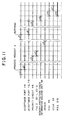
- Fig. 12 is a block diagram showing an information processing device that processes concurrently in response to requests to addresses which do not contend with each other to gain access at high speed.
- the main storage unit 101 stores data sets.
- Numeral 102 is a data processing unit (or CPU) which can execute concurrently and in parallel an operation process and numeral 103 is a data processing unit (or CPU) which can execute concurrently and in parallel an operation process.
- the data processing unit 102 includes a buffer memory unit (BS) 106 and the data processing unit 103 includes a buffer memory unit (BS) 107.
- BS buffer memory unit
- the buffer memory unit 106 includes a data region 108 that holds a piece of data stored in the main storage unit 101 and a tag region 109 that holds tag information including the address of data stored in the data region 108.
- the buffer memory unit 107 includes a data region 110 that holds a piece of data stored in the main storage unit 101 and a tag region 111 that holds tag information including the address of data stored in the data region 110.
- the input/output control unit (IOP) 104 outputs a request to be sent to the data processing units 102 and 103 to the memory control unit 105.
- the memory control unit (MCU) 105 controls data transfer between the main storage unit 101 and the buffer memory units 106 and 107 on a store-in basis.
- the memory control unit 105 includes acceptance ports 112 to 114, a priority circuit 115, a tag copying unit (a second tag unit, TAG 2) 116, an address comparing unit 117, an order issuing unit 118, a response waiting control port 119, and an order response processing unit 120.
- the acceptance port 112 stores a process request from the data processing unit 102; the acceptance port 113 stores a process request from the acceptance port 103; and the acceptance port 114 stores a process request from the input/output control unit 104.
- the priority circuit 115 outputs selectively either one of process requests from the acceptance ports 112 to 114.
- the tag copying unit 116 stores the copies of the tag regions 109 and 111 in the buffer memory unit and then retrieves whether an address corresponding to a process request selected with the priority circuit 115 is stored in the buffer memory unit 106 or 107.
- the address comparing unit 117 compares the address corresponding to a process request selected with the priority circuit 115 with the addresses corresponding to all process requests in a waiting state stored in the acceptance ports 112 to 114.
- the order issuing unit 118 captures the retrieval result (refer to numeral 126 in Fig. 12) from the tag copying unit 116 and the comparison result (refer to numeral 127 in Fig. 12) from the address comparing unit 117, and then issues an order (MCU order) corresponding to a request if either the buffer memory units 102 or 103 stores an address to be processed, or an address corresponding to a process request input from the priority circuit 115 while a block including a target address is not in a response waiting state of an order once issued.
- the order is a general term of a data transfer request or a process request which invalidates entries existing in the buffer memory units 106 and 107, issued from the memory control unit 105 to the buffer memory units 106 and 107.
- the response waiting control port (BCP) 119 sets bits as order-issuing sources respectively corresponding to the data processing units 102 and 103.
- the order response processing circuit 120 inputs a response to an order and then resets a bit corresponding to a request source set by the response control port 119.
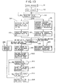
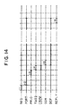
- a process request (or request) issued from the data processing unit 102 (refer to the step A1 shown in Fig. 13 and the duration t1 shown in Fig. 14) is stored in the request acceptance port 112 within the memory control unit 105 (refer to the step A2 in Fig. 13 and the duration t2 shown in Fig. 14).
- the tag copying unit 116 retrieves the address corresponding to the process request (refer to the step A4 shown in Fig. 13 and the duration t4 shown in Fig. 14) to decide whether the address of interest is held in the buffer memory unit 109 or 111 (refer to the step A5 in Fig. 13).
- the address comparing unit 117 compares the address with the process request addresses of all requests (refer to the step A6 in Fig. 13) and decides whether an address of interest is in a waiting state (refer to the step A7 in Fig. 13).
- the order issuing unit 118 receives the retrieval result 126 from the tag copying unit 116 and the comparison result 127 from the address comparing unit 117, and then issues an order in response to the process request when an address of interest exists in either the buffer memory unit 106 or 107 and data block including the address of interest is not in a response waiting state to the order of a data block previously issued (refer to the steps A8 and A9 in Fig. 13 and the duration t5 in Fig. 14).
- a bit (refer to numeral 121 in Fig. 12) which corresponds to the data processing unit of the order issuing source within the response waiting control port 45 is set at the same time when an order corresponding to a process request is issued (refer to the step A10 in Fig. 13).
- the order responding circuit 120 resets the bit 121 in the order issuing unit 118 (refer to the numeral 124 in Fig. 12 and the step A12).
- the response-wait control port 119 After all the bits in the bit 121 have been reset (YES route in the step A13), the response-wait control port 119 outputs a port reset signal (refer to numeral 125 in Fig. 12), thus releasing the acceptance port 112 (refer to the step A14 in Fig. 13).
- the order issuing unit 118 decides that an address of interest exists in the buffer memory unit 106 or 107 and in the waiting state of an order previously issued, based on the retrieval result 126 from the tag copying unit 116 and the comparison result 127 from the address comparing unit 117, it is decided that the order issuing unit 118 cannot issue an order.
- the process request selected by the priority circuit 115 is canceled (refer to the steps A8 to A15 in Fig. 13). Since the acceptance port 112 holds the process request, the priority circuit 115 can select it again (refer to the step A3 in Fig. 13).
- the order issuing unit 118 requests the main storage unit 101 to read out the data block of the address of interest (refer to the step A16 in Fig. 13).
- the response waiting control port 119 outputs a port reset signal 125 to release the acceptance port 112 (refer to the step A14 in Fig. 13).
- a memory protection checking that checks whether an access to a requested address is possible is generally performed to prevent plural programs and data from being destroyed due to an input and output operation.
- the latest data does not exist in a main storage unit, but exists only in the buffer memory unit in the data processing unit.
- a store request in a data unit smaller than the minimum move-out unit in the buffer memory unit is issued from the input/output control unit to the main storage unit, a data block with an address to be subjected to a store request must be moved from the data processing unit to the main storage unit before data is stored from the input/output control unit to the main storage unit.
- the input/output control unit stores data to the main storage unit after both the result of the memory protection checking and the retrieval result of the tag copying unit (the second tag region) have been reported.
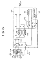
- Fig. 15 is a block diagram showing an information processing device with a memory protection checking function.
- the information processing device includes the main storage unit 101, the data processing units 102 and 103, and the input/output control unit 104, each of which functions in a manner similar to the corresponding element in the information processing device shown in Fig. 12.
- the memory control unit 205 includes the acceptance ports 112 to 114, the priority circuit 115, and the tag copying unit 116, each of which functions in a manner similar to the corresponding element in the memory control unit 105.
- the memory control unit 205 includes a memory protection key storing unit (KSU) 212 which stores data (key) to perform a memory protection check according to a process request from the input/output unit 104.
- KSU memory protection key storing unit
- the process request described above is a store request with a memory protection check to be issued to the main storage unit 101 from the input/output control unit 104 to the memory control unit 205.
- the store request is issued to the data unit smaller than the minimum move-out unit of the buffer memory units 106 or 107 and issued to an address with the latest data to the main storage unit 101.
- the memory protection checking circuit (KCHK) 213 performs a memory protection checking, based on the data for the memory protection check read out of the memory protection key storing unit 212 according to the address corresponding to the process request from the priority circuit 115.
- the priority circuit 115 resumes its selecting operation and at the same time outputs a releasing control signal to the acceptance port 114.
- numeral 216 represents a queue which stores a store request issued from the memory control unit 205 to the main storage unit 101
- 217 represents a priority circuit which selects the priority of the store request.
- the priority circuit 115 selects the store request (refer to the step B3 in Fig. 16 and the duration t23 in Fig. 17), it reads out data used for a memory protection checking (refer to duration t26 in Fig. 17). Then the memory protection checking circuit 213 performs the memory protection checking (refer to the step B4 in Fig. 16 and the duration t27 in Fig. 17).
- the memory protection key storing unit 212 reads out a key corresponding to the address to be subjected to the store request.
- the memory protection checking circuit 213 compares the key with the key-checking key associated with the store request. The result of the memory protection checking is informed to the acceptance port 114. If the access is not allowed (refer to the NO route of the step B4 in Fig. 16), the store request is canceled (in the step B14 in Fig. 16). As a result, the acceptance port 114 is released.
- the acceptance port 114 queues and holds the store request from the input/output control unit 104.
- the priority circuit 115 selects the store request held by the acceptance port 114 (refer to the step B6 in Fig. 16 and the duration t28 shown in Fig. 17)
- the acceptance port 114 is released (in the step B7 in Fig. 16).
- it is decided whether the latest data of the corresponding address exists in the buffer memory unit 106 or 107 in the step B8 in Fig. 16 and the. duration t29 in Fig. 17).
- the store data from the input/output control unit 104 is stored into the main storage unit 101 (in the step B13 shown in Fig. 16).
- the memory control unit 205 issues a move-out order to the data processing unit 102 or 103 having the latest data (refer to the duration t30 shown in Fig. 17).
- the priority circuit 115 takes part in a priority selection (in the step B11 shown in Fig. 16).
- the acceptance port 112 or 113 storing the response is released.
- the main storage unit 101 is accessed with an address corresponding to a store request via the queue 216 and the priority circuit 217. Then the main storage unit 101 stores the move-out data from the data processing unit 102 or 103 (refer to the step B12 in Fig. 16 and the duration t35 in Fig. 17) as well as the store data from the input/output control unit 104 (in the step B13 in Fig. 16).
- an address comparison detects whether the address of a process request selected by the priority circuit 115 is in the contention condition, or in the waiting condition on a request previously issued.
- the memory protection checking process and the retrieving process in the tag copying unit 116 are independently performed along the different flows, as shown in Fig. 17.
- the memory protection checking is performed along the first flow in which the priority circuit 115 selects the store request from the acceptance port 114.
- the tag copying unit 116 performs the retrieving process along the flow which starts when the priority circuit 115 selects the store request from the acceptance port 114.
- the tag copying unit 116 cannot be retrieved till the result of the memory protection checking is known, whereby the memory protection key storing unit 212 takes much time to perform the key reading in the memory protection checking operation.
- the retrieval result from the tag copying unit 116 is a hit, the move-out is issued very slowly. This means that the use efficiency is very poor because the memory protection checking rarely inhibits an access operation.
- the acceptance port 114 once stores and holds a store request from the input/output control unit 104 till at least the result of the memory protection checking is known. Moreover, if the memory protection checking shows an allowable access, the store request is maintained till the tag copying unit 116 starts the retrieval process flow. That is, there is a disadvantage in that the acceptance port 114 cannot be released till the memory protection checking at least is ended. Hence, the following request cannot be received for a long time, whereby the use efficiency and the high speed process are degraded.
- An embodiment of the present invention may provide a memory control method which can reduce the amount of hardware and improve the port use efficiency, thus reducing system constructing costs and improving processing speed.
- a further embodiment may provide a memory control device which can reduce the amount of hardware and improve the port use efficiency, again reducing the system constructing costs and improving processing speed.
- the memory control method or the memory control device can set a process request showing flag in the tag copying unit, whereby whether a block including a process request address exists in the buffer memory unit and whether the block is being processed currently are concurrently obtained by retrieving .only the tag copying unit. This feature allows the address comparing circuit to be omitted, thus reducing the system constructing cost.
- the input/output control unit executes a store request to the memory unit, together with a memory protective checking, the referencing process to the store request of the tag copying unit is performed in synchronism with the memory protective checking of the memory protective deciding means.
- the memory protective checking cannot inhibit an accessing or a hit or erroneous hit is found in the tag copying unit, a high speed storing operation into the storage unit can be established.
- this feature enables a large processing speed, a high port-use efficiency, and a large system throughput.
- numeral 1 represents a data storage unit and 2 represents at least one of data processing units.
- the buffer memory unit 7 includes a data region 3 that holds a piece of data stored in the memory unit 1 and a tag region 4 that holds tag information including the address of data stored in the data region 3.
- the memory control unit 13 controls a data transfer between the memory unit 1 and the buffer memory unit 7 on a store-in basis.
- the memory control unit 13 includes a tag copying unit 5, a port 6, and a process command issuing means 8.
- the tag copying unit 5 holds a part or all of copies in the tag region 4 arranged in the buffer memory unit 7.
- the port 6 holds a process request from the data processing unit 2 or an external process request.
- the process command issuing means 8 refers the tag copying unit 5 and then issues a predetermined process command to the buffer memory unit 7 sent to the data processing unit 2 according to a process request held in the port 6.
- a bit 9 is arranged in the tag copying unit 5 to set a flag showing a process under request to the buffer memory unit 7.
- the process command issuing means 8 includes flag setting means 10 that issues a predetermined process command to be sent to the buffer memory unit 7 to the data processing unit 2 and sets at the same time a flag showing a process under request to the bit 9 in the tag copying unit 5 corresponding to a predetermined process command.
- the tag copying unit 5 has flag setting bits arranged respectively to plural ways.
- the process command issuing means 8 includes port releasing means which releases the port 5 which holds a process request causing an issuance of a predetermined process command at the same time when a predetermined process command sent to the buffer memory unit 7 is issued to the data processing unit 2; and flag resetting means which resets a flag of the tag copying unit 5 corresponding to the process completion report when the process completion report is received from the data processing unit 2 in response to a predetermined process command.
- the process command issuing means 8 can issue a predetermined process command to be sent to the buffer memory unit 7 to the data processing unit 2, on condition that all flags of the portion to be processed under a predetermined process command in the tag copying unit 5 are in a reset state.
- the next process of a process request starts on condition that the flag reset means resets all the flags set in the tag copying unit 5 at an issuance of a predetermined process command.
- the process command issuing means 8 includes a counter that sets the number of responses to be issued, as non-response number, from the data processing unit 2 according to the predetermined process command at the same time when a predetermined process command is issued to the buffer memory unit 7, and subtracting means that subtracts the non-response number from the counter every time when the data processing unit 2 receives a process completion report as a response to a predetermined process command.
- the next process of the process request can be started at the time when the counter counts non-response number of zero.
- the memory control unit 13 issues a predetermined request to the buffer memory unit 7 within the data processing unit 2 while it refers the tag copying unit 5 according to the process request held in the port 6, thus controlling the data holding state of the buffer memory unit 7 on a store-in basis.
- a predetermined process command to be sent to the buffer memory unit 7 is issued to the data processing unit 2 while a flag which shows being in a process request to a portion in the tag copying unit 5, the portion to be processed under the predetermined process command, is set to the bit 9 in the tag copying unit 5.
- the buffer memory unit 7, which has plural ways managed on a set-associative basis, sets a flag to the tag copying unit 5 in every way so that whether a process is being required in each way can be managed.
- a predetermined process request is issued to the buffer memory unit 7 via the data processing unit 2 while the port releasing unit can release the port 6 which holds a process request causing an issuance of the predetermined command.
- the flag resetting means When the flag resetting means receives a process completion report from the data processing unit 2 in response to a predetermined process command, it resets the flag of the tag copying unit 5 corresponding to the process completion report.
- the process command issuing means 8 issues a predetermined process command to the buffer memory unit 7, on condition that all the flags of the portions corresponding to the predetermined process command in the tag copying unit 5 are in a reset state.
- the next process of the process request starts, on condition that the flag resetting means has reset all the flags set in the tag copying unit 5 at an issuing time of the predetermined process request, in response to a process completion report.
- a counter sets the number of responses, as non-response number, to be sent from the data processing unit 2 in response to a predetermined process command at the same time when the process command issuing means issues a predetermined process command to the buffer memory unit 7.
- the subtracting means subtracts the non-response number counted by the counter every time the process command issuing means receives a process request in response to a predetermined process request.
- the process command issuing means controls to start the next process of the process request. Hence the next process can be immediately started according to the condition of the response from the data processing unit 2.
- a predetermined process request to be sent to the buffer memory unit 7 is issued to the data processing unit 2 while the port which holds the process request causing the issuance of the predetermined process command can be released.
- the address holding operation is not needed till the data processing unit 2 completes the response operation.
- the improved port-use efficiency can increase the throughput without increasing the number of ports.
- the next process can be started according to the response condition to a process request, whereby the throughput can be realized advantageously.
- Fig. 2 is a block diagram showing an aspect of the present invention.
- the information processing system includes a storage unit 11 for storing data, at least one of data processing units 2 that operates according to the data from the storage unit 11, an input/output control unit 15 that issues a store request to the storage unit 11, together with a memory protection checking command, and a memory control unit 14.
- Each data processing unit 12 includes a buffer memory unit 18 which consists of a data region 16 which holds a piece of data stored in the storage unit 11, and a tag region 17 which holds tag information including the address of data held in the data region 16.
- the memory control unit 14 includes a tag copying unit 19 and a port 20, and memory protection deciding means 21.
- the tag copying unit 19 holds a part or all of the copy of the tag region 17 arranged in the buffer memory unit 18.
- the port 20 holds a process request issued from the data processing unit 12 or the input/output control unit 15.
- the memory protection deciding means 21 performs a memory protection checking operation when it receives a store request associated with a memory protection checking command from the input/output control unit 15, to the memory unit 11.
- the memory control unit 14 issues a predetermined process request sent to the buffer memory unit 18 to the data processing unit 12, based on the comparison result from the tag copying unit 18 in response to the process request held in the port 20.
- the memory control unit 14 controls the data transfer between the storage unit 11 and the buffer memory control unit 18 on a store-in basis, and allows a store request to be transferred from the input/output control unit 15 to the storage unit 11, according to the result of the memory protection checking from the memory protection deciding means 20.
- the tag copying unit 19 when the input/output control unit 15 outputs a store request associated with a memory protection checking to be sent to the storage unit 11 to the memory control unit 14, the tag copying unit 19 performs a referencing process, in synchronism with the memory protection checking operation of the memory protection deciding unit 21.
- the memory control unit 14 issues a predetermined process command to the buffer memory unit 18 arranged in the data processing unit 12, based on the reference result from the tag copying unit 19 in response to the process request held in the port 20.
- the memory control unit 14 also controls the data holding state of the buffer memory unit 18 on a store-in basis and decides whether a store request is issued from the input/output deciding means 21 to the storage unit 11, based on the result of the memory protection checking operation from the memory protection deciding means 21.
- the input/output control unit 15 issues a store request to be sent to the storage unit 11 to the memory control unit 14, the store request being associated with a memory protection checking command
- the referencing process of the tag copying unit 19 is performed in synchronism with the memory protection checking operation of the memory protection deciding means 21.
- the memory control method when the input/output control unit 15 issues a store request to the storage unit 11, together with a memory protection checking request, the referencing process of the tag copying unit 19 on the store request is performed in synchronism with the memory protection checking operation of the memory protection deciding means 21.
- the storage unit 11 can perform a high speed storing operation, whereby the use efficiency of the port can be improved.
- the above-mentioned procedure contributes largely to an improved system throughput.
- Fig. 3 is a block diagram showing what is claimed in said parent application according to Fig. 1.
- the information processing system includes a main storage unit (MSU) 101, two data processing units (central. processing units (CPUs)) 106 and 107, and an input/output control unit (IOP) 104.
- MSU main storage unit
- CPUs central. processing units
- IOP input/output control unit
- the main storage unit 101 stores data.
- the data processing units 106 and 107 can execute concurrently a parallel data operating process.
- the data processing unit 106 includes a data region that holds a piece of data stored in the main storage unit 101 and a tag region 109 that holds tag information holding tag information with the address of data held in the data region 108.
- the data processing unit 107 includes a data region that holds a piece of data stored in the main storage unit 101 and a tag region 111 that holds tag information holding tag information with the address of data held in the data region 110.
- the buffer memory unit 106 in the data processing unit 102 is managed, for example, on a 4-way set-associative basis.
- the buffer memory unit 107 in the data processing unit 103 is managed, for example, on a 4-way set-associative basis.
- the input/output control unit 104 outputs a process request (process command) to be issued to the external processing units 102 and 103 to the memory control unit 31 (to be described later).
- Numeral 31 represents a memory control unit (MCU) that controls the data transfer between the main storage unit 101 and the buffer memory unit 106 or 107 on a store-in basis. Like the memory control unit 105 shown in Fig. 13, the memory control unit 31 includes acceptance ports 112 to 114 and a priority circuit 115.
- MCU memory control unit
- the acceptance port 112 stores an external process command input from the data processing unit 102.
- the acceptance port 113 stores an external process command input from the data processing unit 103.
- the acceptance port 114 stores an external process command input from the input/output control unit 104.
- the priority circuit 115 outputs selectively any one of the processing commands from the acceptance ports 112 to 114.
- Numeral 32 represents a second tag region.
- the second tag regions (tag copying units) 32 hold a copy of a part or all of the tag region 109 in the buffer memory unit 106 and a copy of a part or all of the tag region 111 in the buffer memory unit 107, respectively.
- flag setting bits are respectively arranged to four ways in the second tag region 32.
- Numeral 33 represents order issuing means (or process command issuing means).
- the order issuing means 33 references the second tag region 32 in response to the tag retrieval result reporting signal 32-1, according to a process command held in each of the acceptance ports 112 to 114, and then issues a predetermined process command (order) 33-1 to be sent respectively to the buffer memory units 106 and 107, to the data processing units 102 and 103.
- a bit 41 showing being under a process request to the buffer memory units 106 and 107 is set to each of the entries in the second tag region 32 (to "1" at a flag setting time).
- the order issuing unit 33 also includes a flag setting function unit (flag setting means) 33A which issues a process request to the buffer memory unit 106 or 107 to the corresponding data processing unit 102 or 103 while it outputs a flag setting control signal 33-2 to the second tag region 32, whereby a flag "1" showing under a process request is set to the bit 41 of the portion (entry) of interest in the second tag region 32.
- a flag setting function unit flag setting means
- the order issuing unit 33 includes a port releasing unit (port releasing means) 33B that outputs the port reset signal 33-3, together with the flag setting control signal 33-2, thus releasing one of the ports 112 to 114 holding a process command.
- a port releasing unit port releasing means
- each of the second tag regions 32 includes a comparison address portion 42 to be compared and a control bit 43 such as valid and exclusive, in addition to the flag 41.
- Numeral 37 represents a responding circuit (flag resetting means).
- the responding circuit 37 receives the response 102-1 from the data processing unit 102 and the response 103-1 from the data processing unit 103 according to the process command already processed in the order issuing unit 33, it outputs a flag reset signal 37-1 to the second flag unit 32.
- the flag of the way of interest is reset while the process completion report 37-2 is output to the counter subtracting circuit 38 (to be described later).
- the order issuing unit 33 issues the buffer memory unit 106 or 107 to the corresponding data processing unit 102 or 103, on condition that all the flags of the portions corresponding to a predetermined process command in the second tag region 32 have been reset.
- the memory control unit 31 starts the next process of a process request, on condition that the response processing circuit 37 has reset all flags set to the second tag region 32 when the previous process command is issued.
- Numeral 35 represents a response waiting control port (BCP).
- the response waiting control port 35 includes a counter 36 that sets the number of responses, as non-response number, to be issued from the data processing unit 102 or 103, or a process command issuing source, corresponding to a process command.
- Numeral 38 represents a counter subtracting circuit (subtracting means).
- the counter subtracting circuit 38 outputs a signal 38-1 to the response waiting control port 35 every time the process completion report 37-2 as a response signal from the data processing unit 102 or 103 is received from the response processing circuit 37, thus subtracting the number of responses not counted by the counter 36.
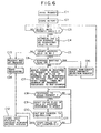
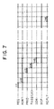
- the memory control unit 31 stores the process command 102-2 in the acceptance port 112 (refer to the step C2 in Fig. 6 and the duration t12 in Fig. 7).
- the priority circuit 115 selects a process request 102-2 (refer to YES route in the step C3 in. Fig. 6 and. the duration t13 in Fig. 7), it retrieves the second tag region 32 using the address corresponding to the process command (refer to the step C4 in Fig. 6 and the duration t14 in Fig. 7) to report the order issuing unit 33 of the retrieval result as a tag retrieval result reporting signal 32-1.
- the tag retrieval result reporting signal 32-1 includes a signal showing whether a process command address including block exists in the buffer memory units 106 and 107 and a signal showing whether a block storing way is in a process request waiting state (a signal corresponding to a flag set in the bit 41).
- the order issuing unit 33 selects the corresponding buffer memory unit 106 or 107 to issue the order 33-1 (refer to the duration t15 in Fig. 7).
- the flag setting unit 33A within the order issuing unit 33 outputs the flag setting control signal 33-2 to set a flag "1" showing being under a process request to the bit 41 of a portion of interest in the second tag region 32.
- the port releasing unit 33B within the order issuing unit 33 issues the port reset signal 33-3 to release the port 112 holding the process request, thus setting the number of issued orders to the counter 36 within the response waiting control port 35 to set the order number information to the waiting control port 35 (step C7 in Fig. 6).
- the acceptance port 112 released can accept a new request.
- the response processing circuit 37 decides that the response has come from the data processing unit 102 or 103 to output the flag reset signal 37-1 to the second tag region 32, thus resetting a flag of a way of interest (in the step C9 in Fig. 6) while it outputs the process completion report 37-2 as a counter subtraction command to the counter subtracting circuit 38.
- the counter subtracting circuit 38 subtracts the count value of the counter 36 (refer to the numeral 38-1 in Fig. 3 and the step C10 in Fig. 6).
- the counter 36 counting "0" (refer to YES route in the step C11 in Fig. 6 and the duration t16 in Fig. 7) means the responses to all orders issued on a process command. Then the flow goes to the step C12 to continue the process in accordance with the content held in the response waiting control port 35.
- the flag setting unit 33A can set a flag showing a process request to the bit 41 in the second tag region 32. Whether a process request address including block exists in the buffer memory units 106 or 107 and whether the block now is being processed can be recognized concurrently by retrieving the second tag unit 32, whereby an exclusive address comparing circuit is not needed. Hence there is an advantage in that the system constructing cost can be reduced.
- a predetermined process request to the buffer memory unit 106 or 107 is issued to the data processing unit 102 or 103 while the port releasing unit 33B can release the port 114 which holds a process request causing the predetermined process command. It is unnecessary to hold the address till the data processing unit 102 and 103 issue responses. Hence the use efficiency of the acceptance ports 112 to 114 can be improved. The improved throughput can be realized without increasing the number of ports. Hence there is an advantage in that the amount of hardware as well as the system constructing cost can be largely reduced.
- the next process of the process request can be started according to the response state to a process request. Hence the sharply increased throughput can be realized.
- Two data processing units and the buffer memory unit with four ways are used.
- the data processing units and the number of ways of the buffer memory unit should not be limited to a limited number, respectively.
- the data processing units and the buffer memory unit can be applied in a desired number, respectively.
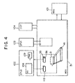
- Fig. 8 is a block diagram showing the said embodiment, which is according to the present invention.
- the information processing system includes two data processing units (CPUs) 102 and 103, an input/output control unit (IOP) 104, a memory control unit (MCU) 51, and a main storage unit (MSU) 101.
- a memory protection checking (where a store request is made to the data unit smaller than the minimum move-out unit of the buffer memory unit 106 or 107 (hereinafter the process request is referred to as a request A)) can be performed to a store request with a memory protection check which is issued from the input/output control unit 104 to the main storage unit 101 via the memory control unit 51.
- the main storage unit 101 and two data processing units 102 and 103, and the input/output control unit 104 have functions in a manner similar to those in the embodiment of the parent application.
- the data processing unit 102 includes a buffer memory unit 106 which consists of the data region 108 and the tag region 109.
- the data processing unit 103 includes a buffer memory unit 107 which consists of the data region 110 and the tag region 111.
- the second tag region (tag copying unit) 52 holds a part or all of a copy of the tag region 109 in the buffer memory unit 106 and a part or all of a copy of the tag region 111 in the buffer memory unit 107.
- the second tag region 52-1 holds a copy of the tag region 109 and the second tag region 52-2 holds a copy of the tag region 111.
- Numeral 53 represents a memory protection key storing unit (KSU).
- the memory protection key storing unit 53 stores data which is used to execute a memory protection checking in response to a process request from the input/output unit 104.
- the memory control unit 51 has the detail configuration shown in Fig. 9.
- the memory control unit 51 includes the second tag region 52 described above, the memory protection key storing unit 53 described above, acceptance ports 112 to 114 being functionally similar to that in the memory control unit 205 in Fig. 15, a priority circuit 115, a queue 216, and a priority circuit 217.
- a predetermined process command such as a move-out order to be sent to the buffer memory unit 106 is issued to the data processing unit 102, together with the associated order number, according to process requests respectively held the acceptance ports 112 to 114 and based on the reference result from the second tag region 52.
- a predetermined process command such as a move-out order to be sent to the buffer memory unit 107 is issued to the data processing unit 103, together with the associated order number, according to process requests respectively held in the acceptance ports 112 to 114 and based on the reference result from the second tag region 52.
- the retrieving process (referencing process) of the second tag region 52 can be performed in synchronism with the memory protection checking of the memory protection checking circuit 54, thus releasing the acceptance port 114.
- the address and the key-checking key in the data block to be subjected to the request A move together with an order issued from the memory control unit 51 or a response issued from the data processing unit 102 or 103 corresponding to the order.
- the memory control unit 51 also includes the memory protection checking circuit (KCHK) 54, or memory protection deciding means, and the memory protection check information holding unit 56.
- KCHK memory protection checking circuit
- the memory protection checking circuit 54 compares the key corresponding to the address of the request A obtained by accessing the memory protection key storing unit 53 with the key-checking key associated with the request A, thus checking whether the requested address is accessible.
- the memory protection checking information holding unit 56 holds information showing whether an order issuance causing request is accompanied by a memory protection checking (or showing the presence or absence of the request A), in order of the order number of an order attached by the memory control unit 51.
- the memory protection checking information holding unit 56 references the order number attached to the response. If it is proved that the response has been made to the request A associated with the memory protection checking, the memory protection checking circuit 54 reads and accesses a key corresponding to the. address associated with the response out of the memory protection key storing unit 53, and then compares the readout key with the key-checking key associated with the response, thus performing a memory protection checking operation.
- the information showing whether an order issuance causing request is associated with a memory protection checking is held in order of the order numbers by the memory protection checking information holding unit 56.
- the information may be associated with the order or the response to the order. In this case, the order number setting operation and the memory protection checking information holding unit 56 can be omitted.
- the acceptance port 114 holds the store request.
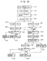
- the input/output control unit 104 issues the request A (refer to the step D1 in Fig. 10 and the duration u1 in Fig. 11) to store the acceptance port 114 in the memory control unit 51 (refer to the step D2 in Fig. 10 and the duration u2 in Fig. 11).
- the priority circuit 115 participates the priority selection (refer to the step D3 in Fig. 10 and the duration u3 in Fig. 11) and then selects the process request (request A) issued from the input/output control unit 104 to the memory control unit 51, together with a memory protection checking operation, the acceptance port 114 is released (step D4 in Fig. 10).
- the retrieving process of the second tag region 52 is performed in synchronism with an access to the memory protection key storing unit 53 (the step D6 in Fig. 10).
- the second tag region 52 is retrieved immediately.
- the access to the memory protection key storing unit 53 takes a relatively long processing time, compared with the retrieval process of the second tag region 52.
- the access to the memory protection key storing unit 53 becomes valid (the step D8 in Fig. 10) so that the memory protection checking circuit 54 performs a memory protection checking (the step D9 in Fig. 10).
- the memory protection checking circuit 54 compares the key-checking key associated with the request A with the key from the memory protection key storing unit 53 and then proves the accessible state (YES route in the step D9 in Fig. 10), the main storage unit 101 stores the store data from the input/output control unit 104 (in the step D10 shown in Fig. 10).
- the memory protection checking circuit 54 performs a memory protection checking and then proves an inaccessible state (NO route in the step D9 in Fig. 10)
- the reset A is canceled (the step D11 in Fig. 10).
- the memory protection checking circuit 54 performs a key checking operation, according to the access result from the memory protection keying unit 53 (the step D9 in Fig. 10), and then invalidates the access by neglecting the checking result.
- the memory control unit 51 issues a move-out order to the data processing unit 102 or 103 which has the latest data in the address corresponding to the request A (refer to the step D12 in Fig. 10 and the duration u6 in Fig. 11).
- An order number is attached to the move-out order transferred to the data processing unit 102 or 103.
- the memory protection check information holding unit 56 holds the instruction by which a memory protection checking is performed to the order number.
- the data processing unit 102 or 103 When the data processing unit 102 or 103 receives the move-out order, it invalidates the tag region 109 or 111 of the corresponding data and then issues the response to the memory control unit 51 to move out the corresponding data (the step D13 in Fig. 10 and the duration u7 in Fig. 11).
- the memory protection checking information holding unit 56 is referenced (refer to the duration u16 in Fig. 11), it is decided whether it is instructed to subject the order number associated with the response to a memory protection checking.
- an access to the memory protection key storing unit 53 is made (refer to the step D16 in Fig. 10 and the duration u10 in Fig. 11) while a move-out data from the data processing unit 102 or 103 is stored into the main storage unit 101 via the queue 216 and the priority circuit 217 (refer to the step D15 in Fig. 10 and the duration u12 in Fig. 11).
- the memory protection checking circuit 54 compares the key-checking key associated with a response with a key from the memory protection key storing unit 53 (refer to the duration u11 in Fig. 11) to permit accessing (YES route in the step D17 in Fig. 10), the move-out data from the data processing unit 102 or 103 is stored in the main storage unit 101 in the step D15. Then the store data from the input/output control unit 104 is stored in the main storage unit 101 (the step D18 in Fig. 10).
- the move-out data from the data processing unit 102 or 103 is stored in the main storage unit 101 in the step D15 but the request A is canceled (the step D19 in Fig. 10).
- the memory protection checking information holding unit 56 corresponding to the order number may hold the result on the memory protection checked in the step D9, without invalidating the checking result of the memory protection checking unit 54.
- the key checking can be omitted in the step D17 in the second flow.
- the key checking result can be obtained merely by referencing the order number associated with a response which is held in the memory protection checking information holding unit 56.
- the input/output control unit 104 requests the memory control unit 51 of a storing process to the main storage unit 101, together with a memory protective checking operation, retrieving the second tag region 52 in response to the store request is performed in synchronism with the memory protection checking process of the memory protection deciding means in the first process flow.
- the memory protection checking is not permitted because of an erroneous hit of the second tag region 52
- the request can be immediately canceled.
- the store request can be made from the input/output control unit 104 to the main storage unit 101 in the same process flow.
- the main storage unit 101 can store the move-out data from the data processing unit 102 or 103 and then stores data from the input/output control unit 104. In the case of no access permission, the main storage unit 101 stores the move-out data from the data processing unit 102 or 103, but the store request according to the request A is canceled.
- the acceptance port 114 which can be released in the first flow can improve the use efficiency, thus contributing largely to the improved system throughput.
- the present embodiment uses two data processing units.
- the number in use of data processing units should not be limited to a specific value, but is applicable to a desired value.
Landscapes
- Engineering & Computer Science (AREA)
- Theoretical Computer Science (AREA)
- Physics & Mathematics (AREA)
- General Engineering & Computer Science (AREA)
- General Physics & Mathematics (AREA)
- Memory System Of A Hierarchy Structure (AREA)
- Techniques For Improving Reliability Of Storages (AREA)
- Multi Processors (AREA)
- Storage Device Security (AREA)
Claims (4)
- Procédé de commande de mémoire destiné à un système de traitement de l'information qui comporte une unité de mémoire (11), une
ou plusieurs unités de traitement de données (12) fonctionnant chacune sur la base de données stockées dans ladite unité de mémoire (11), une unité de commande d'entrée/sortie (15) servant à effectuer une demande de stockage à destination de ladite unité de mémoire (11), en même temps qu'un contrôle de la protection de mémoire, et une unité de commande de mémoire (14) servant à commander le transfert de données entre ladite unité de mémoire (11) et ladite unité de traitement de données (12) ou bien ladite unité de commande d'entrée/sortie (15), chaque dite unité de traitement de données (12) comportant : une unité de mémoire tampon (18) qui possède une région de données (16) servant à maintenir un élément de données stocké dans ladite unité de mémoire (11) ; et une région d'étiquette (17) servant à maintenir des informations d'étiquette comportant l'adresse des données stockées dans ladite région de données (16),
ladite unité de commande de mémoire (14) comportant : une unité de copie d'étiquette (19) servant à maintenir un ou plusieurs éléments d'informations de copie stockés dans ladite région d'étiquette (17) de ladite unité de mémoire tampon (18) ; un port d'accès (20) servant à maintenir une demande de traitement envoyée depuis ladite unité de traitement de données (12) ou ladite unité de commande d'entrée/sortie (15); et un moyen (21 ; 51) de prise de décision de protection de mémoire servant à effectuer un contrôle de protection de mémoire ;
où :caractérisé en ce que ledit moyen (21; 51) de prise de décision de protection de mémoire comporte :lorsque ladite unité de commande de mémoire (14) sélectionne une demande de stockage maintenue par ledit port d'accès (20), ladite unité de commande de mémoire (14) délivre simultanément une demande de traitement de référence de ladite unité de copie d'étiquette (19) à ladite unité de copie d'étiquette (19), et une demande de contrôle de protection de mémoire audit moyen de prise de décision de protection de mémoire (21 ; 51), de façon que ladite unité de commande de mémoire (14) soit autorisée à effectuer ledit traitement de référence de ladite unité de copie d'étiquette (19), en synchronisme avec ledit contrôle de protection de mémoire dudit moyen de prise de décision de protection de mémoire (21 ; 51); etladite unité de commande de mémoire (14) délivre une instruction de traitement prédéterminée à destination de ladite unité de mémoire tampon (18) de ladite unité de traitement de données (12) en fonction de la demande de traitement maintenue par ledit port d'accès (20) et en référence avec un résultat de référence venant de ladite unité de copie d'étiquette (19), commande l'état de maintien de données de ladite unité de mémoire tampon (18) sur la base de ce qui est stocké, et décide si l'unité de commande d'entrée/sortie (15) doit ou non envoyer une demande de stockage envoyée à ladite unité de mémoire (11), sur la base du résultat du contrôle de protection de mémoire venant dudit moyen de prise de décision de protection de mémoire (21; 51);un circuit (54) de contrôle de protection de mémoire servant à contrôler si une adresse demandée est ou non accessible par comparaison d'un code correspondant à une adresse d'une première demande obtenue par accès à une unité (53) de stockage de code de protection de mémoire avec un code de contrôle de code associé à la première demande ;une unité de maintien d'informations de contrôle de protection de mémoire (56) servant à maintenir des informations montrant si une demande ayant amené la délivrance d'un ordre est accompagnée d'un contrôle de protection de mémoire, suivant l'ordre d'un nombre d'ordre d'un ordre fixé par ledit moyen de prise de décision de protection de mémoire (21 ; 51) de lui-même, etle procédé comprenant l'opération qui consiste à contrôler avec ledit moyen de prise de décision de protection de mémoire (21 ; 51), sur la base d'un nombre d'ordre attaché à une réponse, lesdites informations maintenues dans ladite unité (56) de maintien d'informations de contrôle de protection de mémoire et ledit circuit de contrôle de protection de mémoire (54). - Unité de commande de mémoire destinée à un système de traitement de l'information qui comporte une unité de mémoire (11), une ou plusieurs unités de traitement de données (12) fonctionnant chacune sur la base de données stockées dans ladite unité de mémoire (11), une unité de commande d'entrée/sortie (15) servant à effectuer une demande de stockage à destination de ladite unité de mémoire, en même temps qu'un contrôle de protection de mémoire, et une unité de commande de mémoire (14) servant à commander le transfert de données entre ladite unité de mémoire (11) et ladite unité de traitement de données (12) ou ladite unité de commande d'entrée/sortie (15) ; chaque dite unité de traitement de données (12) comportant : une unité de mémoire tampon (18) qui possède une région de données (16) servant à maintenir un élément de données stocké dans ladite unité de mémoire (11); et une région d'étiquette (17) servant à maintenir des informations d'étiquette comportant l'adresse des données stockées dans ladite région de données (16);
ladite unité de commande de mémoire (14) comportant :où:une unité (19) de copie d'étiquette servant à maintenir un ou plusieurs éléments d'informations de copie stockés dans ladite région d'étiquette (17) de ladite unité de mémoire tampon (18);un port d'accès (20) servant à maintenir une demande de traitement envoyée depuis ladite unité de traitement de données (12) ou ladite unité de commande d'entrée/sortie (15) ; etun moyen (21 ; 51) de prise de décision de protection de mémoire, servant à effectuer un contrôle de protection de mémoire ;caractérisé en ce que ledit moyen de prise de décision de protection de mémoire (21 ; 51) comprend :ladite unité de commande de mémoire (14) comprend en outre un circuit de priorité (115) permettant de délivrer simultanément une demande pour un traitement de référence de ladite unité de copie d'étiquette (19) à ladite unité de copie d'étiquette (19) et une demande pour ledit contrôle de protection de mémoire audit moyen de prise de décision de protection de mémoire (21 ; 51) de façon que ladite unité de commande de mémoire (14) soit autorisée à effectuer un traitement de référence de ladite unité de copie d'étiquette (19), en synchronisme avec ledit contrôle de protection de mémoire dudit moyen (21 ; 51) de prise de décision de protection de mémoire ; etladite unité de commande de mémoire (14) délivre une instruction de traitement prédéterminée à l'unité de mémoire tampon (18) de ladite unité de traitement de données (12) en fonction de la demande de traitement maintenue par ledit port d'accès (20) et en référence à un résultat de référence venant de ladite unité de copie d'étiquette (19), commande l'état de maintien de données de ladite unité de mémoire tampon (18) sur la base de ce qui est stocké, et décide si ladite unité de commande d'entrée/sortie (15) doit ou non envoyer la demande de stockage à ladite unité de mémoire (11), sur la base du résultat du contrôle de protection de mémoire venant dudit moyen de prise de décision de protection de mémoire (21 ; 51);un circuit (54) de contrôle de protection de mémoire servant à contrôler si une adresse demandée est ou non accessible par comparaison d'un code correspondant à une adresse d'une première demande obtenue par accès à une unité (53) de stockage de code de protection de mémoire avec un code de contrôle de code associé avec la première demande ; etune unité (56) de maintien d'informations de contrôle de protection de mémoire servant à maintenir des informations montrant si une demande ayant amené la délivrance d'un ordre est accompagnée d'un contrôle de protection de mémoire, dans l'ordre d'un nombre d'ordre d'un ordre fixé par ledit moyen de prise de décision de protection de mémoire (21 ; 51) de lui-même. - Procédé de commande de mémoire destiné à un système de traitement de l'information selon la revendication 1, caractérisé en ce que ledit procédé comprend en outre l'opération qui consiste à libérer ledit port d'accès (20) maintenant ladite demande de stockage qui provoque la délivrance simultanée d'une demande d'un traitement de référence de ladite unité de copie d'étiquette (19) à ladite unité de copie d'étiquette (19), et une demande de contrôle de protection de mémoire audit moyen de prise de décision de protection de mémoire (21 ; 51).
- Unité de commande de mémoire destinée à un système de traitement de l'information selon la revendication 2, caractérisée en ce que ledit circuit de priorité (115) comporte un moyen de libération servant à libérer ledit port d'accès (20) maintenant ladite demande de stockage qui provoque la délivrance simultanée d'une demande d'un traitement de référence de ladite unité de copie d'étiquette (19) à ladite unité de copie d'étiquette (19), et une demande de contrôle de protection de mémoire audit moyen de prise de décision de protection de mémoire (21 ; 51); afin d'effectuer ledit traitement de référence de ladite unité de copie d'étiquette (19) en synchronisme avec ledit contrôle de protection de mémoire dudit moyen de prise de décision de protection de mémoire (21 ; 51).
Applications Claiming Priority (4)
| Application Number | Priority Date | Filing Date | Title |
|---|---|---|---|
| JP11990494A JP3360933B2 (ja) | 1994-06-01 | 1994-06-01 | 情報処理システムにおける記憶制御方法および記憶制御装置 |
| JP11990494 | 1994-06-01 | ||
| JP119904/94 | 1994-06-06 | ||
| EP95302328A EP0690383B1 (fr) | 1994-06-01 | 1995-04-07 | Procédé et dispositif de commande de mémoire appropriés pour un sytème de traitement d'information comportant une unité d'antémémoire |
Related Parent Applications (1)
| Application Number | Title | Priority Date | Filing Date |
|---|---|---|---|
| EP95302328A Division EP0690383B1 (fr) | 1994-06-01 | 1995-04-07 | Procédé et dispositif de commande de mémoire appropriés pour un sytème de traitement d'information comportant une unité d'antémémoire |
Publications (3)
| Publication Number | Publication Date |
|---|---|
| EP0903669A2 EP0903669A2 (fr) | 1999-03-24 |
| EP0903669A3 EP0903669A3 (fr) | 1999-07-28 |
| EP0903669B1 true EP0903669B1 (fr) | 2003-10-22 |
Family
ID=14773096
Family Applications (2)
| Application Number | Title | Priority Date | Filing Date |
|---|---|---|---|
| EP98122596A Expired - Lifetime EP0903669B1 (fr) | 1994-06-01 | 1995-04-07 | Procédé et dispositif de commande de mémoire appropriés pour un système de traitement d'information |
| EP95302328A Expired - Lifetime EP0690383B1 (fr) | 1994-06-01 | 1995-04-07 | Procédé et dispositif de commande de mémoire appropriés pour un sytème de traitement d'information comportant une unité d'antémémoire |
Family Applications After (1)
| Application Number | Title | Priority Date | Filing Date |
|---|---|---|---|
| EP95302328A Expired - Lifetime EP0690383B1 (fr) | 1994-06-01 | 1995-04-07 | Procédé et dispositif de commande de mémoire appropriés pour un sytème de traitement d'information comportant une unité d'antémémoire |
Country Status (4)
| Country | Link |
|---|---|
| US (1) | US5829039A (fr) |
| EP (2) | EP0903669B1 (fr) |
| JP (1) | JP3360933B2 (fr) |
| DE (2) | DE69518473T2 (fr) |
Families Citing this family (12)
| Publication number | Priority date | Publication date | Assignee | Title |
|---|---|---|---|---|
| US6263408B1 (en) * | 1999-03-31 | 2001-07-17 | International Business Machines Corporation | Method and apparatus for implementing automatic cache variable update |
| US20050021947A1 (en) * | 2003-06-05 | 2005-01-27 | International Business Machines Corporation | Method, system and program product for limiting insertion of content between computer programs |
| US9727468B2 (en) * | 2004-09-09 | 2017-08-08 | Intel Corporation | Resolving multi-core shared cache access conflicts |
| US7814166B2 (en) | 2006-01-27 | 2010-10-12 | Sony Computer Entertainment Inc. | Methods and apparatus for virtualizing an address space |
| US8510596B1 (en) | 2006-02-09 | 2013-08-13 | Virsec Systems, Inc. | System and methods for run time detection and correction of memory corruption |
| JP4297969B2 (ja) | 2006-02-24 | 2009-07-15 | 富士通株式会社 | 記録制御装置および記録制御方法 |
| JP4373485B2 (ja) * | 2006-02-28 | 2009-11-25 | 富士通株式会社 | 情報処理装置及び該制御方法 |
| US8904189B1 (en) | 2010-07-15 | 2014-12-02 | The Research Foundation For The State University Of New York | System and method for validating program execution at run-time using control flow signatures |
| JP2016534479A (ja) | 2013-09-12 | 2016-11-04 | ヴァーセック・システムズ・インコーポレーテッドVirsec Systems,Inc. | マルウェアのランタイム中の自動検出 |
| AU2015279920B2 (en) | 2014-06-24 | 2018-03-29 | Virsec Systems, Inc. | Automated root cause analysis of single or N-TIERED applications |
| CN106687981B (zh) | 2014-06-24 | 2020-09-01 | 弗塞克系统公司 | 用于自动化检测输入和输出验证和资源管理漏洞的系统和方法 |
| JP6949951B2 (ja) | 2016-06-16 | 2021-10-13 | ヴァーセック システムズ,インコーポレイテッド | コンピュータアプリケーション内のメモリ破損を修復するためのシステム及び方法 |
Family Cites Families (10)
| Publication number | Priority date | Publication date | Assignee | Title |
|---|---|---|---|---|
| US4503497A (en) * | 1982-05-27 | 1985-03-05 | International Business Machines Corporation | System for independent cache-to-cache transfer |
| ATE80480T1 (de) * | 1985-02-05 | 1992-09-15 | Digital Equipment Corp | Vorrichtung und verfahren zur zugriffsteuerung in einer mehrcachespeicherdatenverarbeitungsanordnung. |
| US4949239A (en) * | 1987-05-01 | 1990-08-14 | Digital Equipment Corporation | System for implementing multiple lock indicators on synchronous pended bus in multiprocessor computer system |
| CA1325289C (fr) * | 1989-02-03 | 1993-12-14 | Digital Equipment Corporation | Methode pour realiser la coherence des donnees entre plusieurs antememoires et la memoire principale d'un ordinateur multiprocesseur |
| US5297269A (en) | 1990-04-26 | 1994-03-22 | Digital Equipment Company | Cache coherency protocol for multi processor computer system |
| US5265232A (en) * | 1991-04-03 | 1993-11-23 | International Business Machines Corporation | Coherence control by data invalidation in selected processor caches without broadcasting to processor caches not having the data |
| US5428761A (en) * | 1992-03-12 | 1995-06-27 | Digital Equipment Corporation | System for achieving atomic non-sequential multi-word operations in shared memory |
| DE69323790T2 (de) * | 1992-04-29 | 1999-10-07 | Sun Microsystems, Inc. | Verfahren und Vorrichtung für mehreren ausstehende Operationen in einem cachespeicherkohärenten Multiprozessorsystem |
| US5398325A (en) * | 1992-05-07 | 1995-03-14 | Sun Microsystems, Inc. | Methods and apparatus for improving cache consistency using a single copy of a cache tag memory in multiple processor computer systems |
| US5434993A (en) * | 1992-11-09 | 1995-07-18 | Sun Microsystems, Inc. | Methods and apparatus for creating a pending write-back controller for a cache controller on a packet switched memory bus employing dual directories |
-
1994
- 1994-06-01 JP JP11990494A patent/JP3360933B2/ja not_active Expired - Lifetime
-
1995
- 1995-04-07 EP EP98122596A patent/EP0903669B1/fr not_active Expired - Lifetime
- 1995-04-07 DE DE69518473T patent/DE69518473T2/de not_active Expired - Lifetime
- 1995-04-07 DE DE69532006T patent/DE69532006T2/de not_active Expired - Lifetime
- 1995-04-07 EP EP95302328A patent/EP0690383B1/fr not_active Expired - Lifetime
-
1997
- 1997-06-05 US US08/869,740 patent/US5829039A/en not_active Expired - Lifetime
Also Published As
| Publication number | Publication date |
|---|---|
| EP0690383A3 (fr) | 1996-06-05 |
| US5829039A (en) | 1998-10-27 |
| DE69532006T2 (de) | 2004-05-19 |
| EP0690383A2 (fr) | 1996-01-03 |
| DE69518473T2 (de) | 2001-01-04 |
| EP0903669A2 (fr) | 1999-03-24 |
| EP0903669A3 (fr) | 1999-07-28 |
| DE69532006D1 (de) | 2003-11-27 |
| JP3360933B2 (ja) | 2003-01-07 |
| EP0690383B1 (fr) | 2000-08-23 |
| JPH07325760A (ja) | 1995-12-12 |
| DE69518473D1 (de) | 2000-09-28 |
Similar Documents
| Publication | Publication Date | Title |
|---|---|---|
| US5490261A (en) | Interlock for controlling processor ownership of pipelined data for a store in cache | |
| US7047322B1 (en) | System and method for performing conflict resolution and flow control in a multiprocessor system | |
| JP3259969B2 (ja) | キャッシュメモリ制御装置 | |
| KR100567099B1 (ko) | L2 디렉토리를 이용한 멀티프로세서 시스템의 가-저장촉진 방법 및 장치 | |
| EP0349122B1 (fr) | Procédé et dispositif de filtrage de demandes d'invalidation | |
| US6249846B1 (en) | Distributed data dependency stall mechanism | |
| EP0608622A1 (fr) | Système multiprocesseur avec antémémoires à niveaux multiples | |
| US6625698B2 (en) | Method and apparatus for controlling memory storage locks based on cache line ownership | |
| JPS6135584B2 (fr) | ||
| EP0903669B1 (fr) | Procédé et dispositif de commande de mémoire appropriés pour un système de traitement d'information | |
| US6119150A (en) | Message passing distributed shared memory system that eliminates unnecessary software controlled cache flushes or purges | |
| JP2002297379A (ja) | ハードウェアプリフェッチシステム | |
| US6105108A (en) | Method and apparatus for releasing victim data buffers of computer systems by comparing a probe counter with a service counter | |
| US11379152B2 (en) | Epoch-based determination of completion of barrier termination command | |
| US5426754A (en) | Cross-interrogate method and means for combined scaler and vector processing system | |
| US7447845B2 (en) | Data processing system, processor and method of data processing in which local memory access requests are serviced by state machines with differing functionality | |
| US6202126B1 (en) | Victimization of clean data blocks | |
| US5623626A (en) | Logical cache memory for multi-processor system | |
| JPH0567976B2 (fr) | ||
| US7447844B2 (en) | Data processing system, processor and method of data processing in which local memory access requests are serviced on a fixed schedule | |
| US6101581A (en) | Separate victim buffer read and release control | |
| US6892257B2 (en) | Exclusive access control to a processing resource | |
| US20010032297A1 (en) | Cache memory apparatus and data processing system | |
| US12038839B2 (en) | Processor and method for designating a demotion target to be demoted from an in-core cache structure to an out-of-core cache structure | |
| US7080205B2 (en) | Arrangement and method for reducing the processing time of a data processing device |
Legal Events
| Date | Code | Title | Description |
|---|---|---|---|
| PUAI | Public reference made under article 153(3) epc to a published international application that has entered the european phase |
Free format text: ORIGINAL CODE: 0009012 |
|
| AC | Divisional application: reference to earlier application |
Ref document number: 690383 Country of ref document: EP |
|
| AK | Designated contracting states |
Kind code of ref document: A2 Designated state(s): DE GB |
|
| PUAL | Search report despatched |
Free format text: ORIGINAL CODE: 0009013 |
|
| AK | Designated contracting states |
Kind code of ref document: A3 Designated state(s): DE GB |
|
| 17P | Request for examination filed |
Effective date: 19990705 |
|
| 17Q | First examination report despatched |
Effective date: 20010514 |
|
| RIC1 | Information provided on ipc code assigned before grant |
Free format text: 7G 06F 12/08 A, 7G 06F 11/00 B |
|
| RTI1 | Title (correction) |
Free format text: MEMORY CONTROL METHOD AND APPARATUS SUITABLE FOR INFORMATION PROCESSING SYSTEM |
|
| GRAH | Despatch of communication of intention to grant a patent |
Free format text: ORIGINAL CODE: EPIDOS IGRA |
|
| DAX | Request for extension of the european patent (deleted) | ||
| RIC1 | Information provided on ipc code assigned before grant |
Ipc: 7G 06F 11/00 B Ipc: 7G 06F 12/08 A |
|
| RTI1 | Title (correction) |
Free format text: MEMORY CONTROL METHOD AND APPARATUS SUITABLE FOR INFORMATION PROCESSING SYSTEM |
|
| GRAS | Grant fee paid |
Free format text: ORIGINAL CODE: EPIDOSNIGR3 |
|
| GRAA | (expected) grant |
Free format text: ORIGINAL CODE: 0009210 |
|
| AC | Divisional application: reference to earlier application |
Ref document number: 0690383 Country of ref document: EP Kind code of ref document: P |
|
| AK | Designated contracting states |
Kind code of ref document: B1 Designated state(s): DE GB |
|
| REG | Reference to a national code |
Ref country code: GB Ref legal event code: FG4D |
|
| REF | Corresponds to: |
Ref document number: 69532006 Country of ref document: DE Date of ref document: 20031127 Kind code of ref document: P |
|
| PLBE | No opposition filed within time limit |
Free format text: ORIGINAL CODE: 0009261 |
|
| STAA | Information on the status of an ep patent application or granted ep patent |
Free format text: STATUS: NO OPPOSITION FILED WITHIN TIME LIMIT |
|
| 26N | No opposition filed |
Effective date: 20040723 |
|
| PGFP | Annual fee paid to national office [announced via postgrant information from national office to epo] |
Ref country code: DE Payment date: 20130403 Year of fee payment: 19 Ref country code: GB Payment date: 20130403 Year of fee payment: 19 |
|
| REG | Reference to a national code |
Ref country code: DE Ref legal event code: R119 Ref document number: 69532006 Country of ref document: DE |
|
| GBPC | Gb: european patent ceased through non-payment of renewal fee |
Effective date: 20140407 |
|
| REG | Reference to a national code |
Ref country code: DE Ref legal event code: R119 Ref document number: 69532006 Country of ref document: DE Effective date: 20141101 |
|
| PG25 | Lapsed in a contracting state [announced via postgrant information from national office to epo] |
Ref country code: GB Free format text: LAPSE BECAUSE OF NON-PAYMENT OF DUE FEES Effective date: 20140407 Ref country code: DE Free format text: LAPSE BECAUSE OF NON-PAYMENT OF DUE FEES Effective date: 20141101 |