EP0903429B1 - Process for producing heavily doped silicon - Google Patents
Process for producing heavily doped silicon Download PDFInfo
- Publication number
- EP0903429B1 EP0903429B1 EP98115709A EP98115709A EP0903429B1 EP 0903429 B1 EP0903429 B1 EP 0903429B1 EP 98115709 A EP98115709 A EP 98115709A EP 98115709 A EP98115709 A EP 98115709A EP 0903429 B1 EP0903429 B1 EP 0903429B1
- Authority
- EP
- European Patent Office
- Prior art keywords
- doped
- double
- crystal
- doping
- ionic radius
- Prior art date
- Legal status (The legal status is an assumption and is not a legal conclusion. Google has not performed a legal analysis and makes no representation as to the accuracy of the status listed.)
- Expired - Lifetime
Links
Images

Classifications
-
- C—CHEMISTRY; METALLURGY
- C30—CRYSTAL GROWTH
- C30B—SINGLE-CRYSTAL GROWTH; UNIDIRECTIONAL SOLIDIFICATION OF EUTECTIC MATERIAL OR UNIDIRECTIONAL DEMIXING OF EUTECTOID MATERIAL; REFINING BY ZONE-MELTING OF MATERIAL; PRODUCTION OF A HOMOGENEOUS POLYCRYSTALLINE MATERIAL WITH DEFINED STRUCTURE; SINGLE CRYSTALS OR HOMOGENEOUS POLYCRYSTALLINE MATERIAL WITH DEFINED STRUCTURE; AFTER-TREATMENT OF SINGLE CRYSTALS OR A HOMOGENEOUS POLYCRYSTALLINE MATERIAL WITH DEFINED STRUCTURE; APPARATUS THEREFOR
- C30B29/00—Single crystals or homogeneous polycrystalline material with defined structure characterised by the material or by their shape
- C30B29/02—Elements
- C30B29/06—Silicon
-
- C—CHEMISTRY; METALLURGY
- C30—CRYSTAL GROWTH
- C30B—SINGLE-CRYSTAL GROWTH; UNIDIRECTIONAL SOLIDIFICATION OF EUTECTIC MATERIAL OR UNIDIRECTIONAL DEMIXING OF EUTECTOID MATERIAL; REFINING BY ZONE-MELTING OF MATERIAL; PRODUCTION OF A HOMOGENEOUS POLYCRYSTALLINE MATERIAL WITH DEFINED STRUCTURE; SINGLE CRYSTALS OR HOMOGENEOUS POLYCRYSTALLINE MATERIAL WITH DEFINED STRUCTURE; AFTER-TREATMENT OF SINGLE CRYSTALS OR A HOMOGENEOUS POLYCRYSTALLINE MATERIAL WITH DEFINED STRUCTURE; APPARATUS THEREFOR
- C30B15/00—Single-crystal growth by pulling from a melt, e.g. Czochralski method
- C30B15/02—Single-crystal growth by pulling from a melt, e.g. Czochralski method adding crystallising materials or reactants forming it in situ to the melt
- C30B15/04—Single-crystal growth by pulling from a melt, e.g. Czochralski method adding crystallising materials or reactants forming it in situ to the melt adding doping materials, e.g. for n-p-junction
-
- C—CHEMISTRY; METALLURGY
- C30—CRYSTAL GROWTH
- C30B—SINGLE-CRYSTAL GROWTH; UNIDIRECTIONAL SOLIDIFICATION OF EUTECTIC MATERIAL OR UNIDIRECTIONAL DEMIXING OF EUTECTOID MATERIAL; REFINING BY ZONE-MELTING OF MATERIAL; PRODUCTION OF A HOMOGENEOUS POLYCRYSTALLINE MATERIAL WITH DEFINED STRUCTURE; SINGLE CRYSTALS OR HOMOGENEOUS POLYCRYSTALLINE MATERIAL WITH DEFINED STRUCTURE; AFTER-TREATMENT OF SINGLE CRYSTALS OR A HOMOGENEOUS POLYCRYSTALLINE MATERIAL WITH DEFINED STRUCTURE; APPARATUS THEREFOR
- C30B23/00—Single-crystal growth by condensing evaporated or sublimed materials
- C30B23/02—Epitaxial-layer growth
-
- C—CHEMISTRY; METALLURGY
- C30—CRYSTAL GROWTH
- C30B—SINGLE-CRYSTAL GROWTH; UNIDIRECTIONAL SOLIDIFICATION OF EUTECTIC MATERIAL OR UNIDIRECTIONAL DEMIXING OF EUTECTOID MATERIAL; REFINING BY ZONE-MELTING OF MATERIAL; PRODUCTION OF A HOMOGENEOUS POLYCRYSTALLINE MATERIAL WITH DEFINED STRUCTURE; SINGLE CRYSTALS OR HOMOGENEOUS POLYCRYSTALLINE MATERIAL WITH DEFINED STRUCTURE; AFTER-TREATMENT OF SINGLE CRYSTALS OR A HOMOGENEOUS POLYCRYSTALLINE MATERIAL WITH DEFINED STRUCTURE; APPARATUS THEREFOR
- C30B25/00—Single-crystal growth by chemical reaction of reactive gases, e.g. chemical vapour-deposition growth
- C30B25/02—Epitaxial-layer growth
-
- C—CHEMISTRY; METALLURGY
- C30—CRYSTAL GROWTH
- C30B—SINGLE-CRYSTAL GROWTH; UNIDIRECTIONAL SOLIDIFICATION OF EUTECTIC MATERIAL OR UNIDIRECTIONAL DEMIXING OF EUTECTOID MATERIAL; REFINING BY ZONE-MELTING OF MATERIAL; PRODUCTION OF A HOMOGENEOUS POLYCRYSTALLINE MATERIAL WITH DEFINED STRUCTURE; SINGLE CRYSTALS OR HOMOGENEOUS POLYCRYSTALLINE MATERIAL WITH DEFINED STRUCTURE; AFTER-TREATMENT OF SINGLE CRYSTALS OR A HOMOGENEOUS POLYCRYSTALLINE MATERIAL WITH DEFINED STRUCTURE; APPARATUS THEREFOR
- C30B31/00—Diffusion or doping processes for single crystals or homogeneous polycrystalline material with defined structure; Apparatus therefor
-
- H—ELECTRICITY
- H10—SEMICONDUCTOR DEVICES; ELECTRIC SOLID-STATE DEVICES NOT OTHERWISE PROVIDED FOR
- H10D—INORGANIC ELECTRIC SEMICONDUCTOR DEVICES
- H10D62/00—Semiconductor bodies, or regions thereof, of devices having potential barriers
- H10D62/80—Semiconductor bodies, or regions thereof, of devices having potential barriers characterised by the materials
- H10D62/83—Semiconductor bodies, or regions thereof, of devices having potential barriers characterised by the materials being Group IV materials, e.g. B-doped Si or undoped Ge
- H10D62/834—Semiconductor bodies, or regions thereof, of devices having potential barriers characterised by the materials being Group IV materials, e.g. B-doped Si or undoped Ge further characterised by the dopants
Definitions
- the present invention relates to a method of producing a metallic Si single crystal having low resistivity useful as a substrate for semiconductor devices such as LSI or super LSI.
- Si has been used as a substrate material for semiconductor devices such as LSI or super LSI.
- An n-type semiconductor having electrons serving as a carrier is obtained by doping Si with an n-type dopant, while a p-type semiconductor having holes serving as a carrier is obtained by doping Si with a p-type dopant.
- Each semiconductor is fabricated to a semiconductor device bestowed with various properties designed for a specified use.
- a thin metal film such as Au or Al useful for wiring is vapor-deposited on a Si substrate.
- Si itself can not be used as for wiring due to great resistivity even in case of n-type or p-type Si.
- Minute wiring can not be formed from the thin metal film.
- metal atoms diffused from the thin film to a semiconductor region cause a deep level, resulting in reduction of carriers by recombination.
- the metal film puts restriction on integration of semiconductor devices with high density.
- a demand for provision of semiconductor devices with good performance but small in size becomes stronger and stronger in these days. Such the demand can not be attained by conventional methods due to the restriction.
- Applied Physics Letters, Vol. 52, No. 16, pages 1335-1337, 1988 describes that lattice defects in boron highly doped silicon molecular beam epitaxy films (B: 2 ⁇ 10 20 cm -3 ) are reduced by a simultaneous doping of germanium and boron.
- strain compensation considerably reduces dislocation generation in the diffused layers. This strain compensation is brought about because impurities such as tin and boron, or tin and phosphorus, have been diffused simultaneously into the silicon, with tin counteracting the stresses produced by the solute lattice contraction of the boron or the phosphorus.
- US-A-5 553 566 describes a method for fabricating semiconductor substrates with resistivity below 0.02 ohm-cm. This low resistivity is achieved by doping a silicon melt with a phosphorous concentration above 1 ⁇ 10 18 .
- the silicon melt is also doped with the germanium concentration that is 1.5 to 2.5 times that of the phosphorous concentration.
- US-A-4 631 234 describes a substitutionally strengthened silicon semiconductor material. A high concentration of germanium atoms is added to a silicon melt to thereby substitutionally displace various silicon atoms throughout the crystalline structure. The germanium atoms, being larger than the silicon atoms, block crystalline dislocations and thus localize such dislocations so that a fault line does not spread throughout the crystalline structure. In heavily boron doped P + silicon substrates, the larger germanium atoms offset the crystalline shrinkage caused by the boron atoms, thereby equilibrating the silicon crystal size.
- the present invention is aimed at provision of heavily-doped silicon which is useful itself for wiring semiconductors.
- the object of the present invention is to provide a metallic Si single crystal having resistivity sufficiently lowered to a level useful as wiring.
- the growth of the heavily-doped Si single crystal may be performed by any of a pulling method, an epitaxy method or a selective diffusion method.
- molecular X and Y beams together with atomic Si beam are simultaneously ejected by MBE (a molecular beam epitaxy method), MOCVD (a metal organic chemical vapor deposition method) or the like for epitaxial growth.
- MBE molecular beam epitaxy method
- MOCVD metal organic chemical vapor deposition method
- vapor-deposited elements X and Y are both diffused to a substrate by annealing, so as to form a region double-doped with the elements X and Y.
- P is representatively used as the element X
- B is representatively used as the element Y.
- such combination of the elements X and Y does not put any limitation on the scope of the present invention.
- the other combination of the elements X and Y also enables heavy-doping.
- concentration of the dopant is approximately 10 19 /cm 3 at most. Even if much more amount of P or B is added to Si, number of carriers can not be increased due to increase of lattice defects That is, since an substitutional atomic position of Si is not replaced by P or B, a trap center is realized due to appearance of atomic vacancy of Si and an atom is inserted to an interstitial position. As a result, resistivity of the doped Si is not lowered any more.
- concentration of the dopants can be increased to a level exceeding 10 20 /cm 3 .
- concentration of the dopants can be increased to a level exceeding 10 20 /cm 3 .
- the inventor suppose the effect of the double-doping on increase of concentration as follows:
- Si is double-doped with P (whose ionic radius is larger than Si) and B (whose ionic radius is smaller than Si)
- a strain energy of Si is relaxed so that Si can be heavily-doped up to high concentration without accumulation of strain. Consequently, the Si single crystal is heavily-doped up to high concentration without any lattice default.
- the element X serving as a donor and the element Y serving as an acceptor are charged at positive (+) and negative (-) potentials; respectively, so as to enable coexistence of n-type and p-type dopants.
- a Coulomb force between the n-type and p-type dopants reduces an electrostatic energy, resulting in stabilization of crystallographic structure.
- Double-doping with P and B at an atomic ratio of (1+ ⁇ ):1 under such condition effectively promotes growth of a n-type Si crystal having low resistivity and including electrons as a carrier. While, double-doping with P and B at an atomic ratio of 1:(1+ ⁇ ) promotes growth of a p-type Si crystal including holes as a carrier.
- the Si crystal can be heavily-doped up to high concentration exceeding 10 20 /cm 3 , although compared concentration is approximately 10 19 /cm 3 or so at most by conventional sole P or B doping.
- the Si crystal heavily-doped in this way exhibits metallic property but not dielectric property. That is, the heavily-doped Si has a sufficiently low resistivity in an order of 10 -2 -10 -5 ⁇ -cm, so that the heavily-doped Si itself is useful as a wiring material for electrically connecting various semiconductor devices without necessity of a thin metal film such as Au or Al.
- a Si material was inserted in a crucible 2 located in a vacuum chamber 1 .
- the Si material was heated up to 1550°C by a high-frequency induction heater 3 and melted to prepare a Si melt 4 .
- the Si melt 4 was mixed with P and B.
- Addition amount of P was adjusted at 6 ⁇ 10 20 /cm 3 , 1 ⁇ 10 22 /cm 3 , 2 ⁇ 10 22 /cm 3 and 6 ⁇ 10 22 /cm 3 , while an amount of B was controlled to a half of an equivalency to the corresponding amount of P.
- a seed crystal 5 was brought in contact with the Si melt 4 .
- the seed crystal 5 was rotated and gradually lifted up at a speed of 1 cm/hour to grow a Si single crystal 6 from the Si melt 4 .
- a molecular beam epitaxy device was used in Example 2 for double-doping a Si layer, which was grown up according to a vapor-phase epitaxy method, with P and B.
- a Si substrate 12 was set in a vacuum chamber 11 held in an evacuated atmosphere at a degree of vacuum of 1.3 ⁇ 10 -8 Pa as shown in Fig. 4.
- An atomic Si beam activated by a high-frequency induction heater 13 was supplied to the vacuum chamber at a partial pressure of 1.3 ⁇ 10 -4 Pa, so as to epitaxially grow a Si crystal 14 on the Si substrate 12.
- a B beam 17 and a P beam 18 each activated by heaters 15 and 16, respectively, were supplied to the vacuum chamber 11 .
- P serving as a donor 22 together with B serving as an acceptor 23 was vapor deposited on a Si singe crystal substrate 21, as shown in Fig. 4. Thereafter, the substrate 21 was annealed at 1200°C in a furnace to diffuse P and B into the Si crystal. Due to diffusion of P and B, a region 24 double-doped with P and B was formed in the Si single crystal substrate 21, as shown in Fig. 5.
- a Si crystal is double-doped with at least one element X whose ionic radius is larger than Si together with at least one element Y selected from B, Al, Ga and In whose ionic radius is smaller than Si at an atomic ratio of 1:(1+ ⁇ ) or (1+ ⁇ ):1 with the provision of ⁇ being a value of 1-5.
- the double doping remarkably increases the number of carriers up to 10 20 -10 22 /cm 3 , although a number of carriers in a doped Si according to a conventional method is approximately 10 19 /cm 3 or so at most.
- the Si heavily-doped in this way has sufficiently low resistivity as compared with conventional n-type or p-type Si. Due to the low resistivity, the double-doped Si itself is useful as a wiring material without deposition of a thin metal film such as Au or Al, and semiconductor devices can be integrated with extremely high density.
Landscapes
- Chemical & Material Sciences (AREA)
- Engineering & Computer Science (AREA)
- Crystallography & Structural Chemistry (AREA)
- Materials Engineering (AREA)
- Metallurgy (AREA)
- Organic Chemistry (AREA)
- Chemical Kinetics & Catalysis (AREA)
- General Chemical & Material Sciences (AREA)
- Crystals, And After-Treatments Of Crystals (AREA)
- Physical Deposition Of Substances That Are Components Of Semiconductor Devices (AREA)
- Electrodes Of Semiconductors (AREA)
- Internal Circuitry In Semiconductor Integrated Circuit Devices (AREA)
- Liquid Deposition Of Substances Of Which Semiconductor Devices Are Composed (AREA)
- Silicon Compounds (AREA)
Description
- The present invention relates to a method of producing a metallic Si single crystal having low resistivity useful as a substrate for semiconductor devices such as LSI or super LSI.
- Si has been used as a substrate material for semiconductor devices such as LSI or super LSI. An n-type semiconductor having electrons serving as a carrier is obtained by doping Si with an n-type dopant, while a p-type semiconductor having holes serving as a carrier is obtained by doping Si with a p-type dopant. Each semiconductor is fabricated to a semiconductor device bestowed with various properties designed for a specified use.
- When a circuit is built up between fabricated semiconductor devices, a thin metal film such as Au or Al useful for wiring is vapor-deposited on a Si substrate. However, Si itself can not be used as for wiring due to great resistivity even in case of n-type or p-type Si.
- Minute wiring can not be formed from the thin metal film. Besides, metal atoms diffused from the thin film to a semiconductor region cause a deep level, resulting in reduction of carriers by recombination. In short, the metal film puts restriction on integration of semiconductor devices with high density. On the other hand, a demand for provision of semiconductor devices with good performance but small in size becomes stronger and stronger in these days. Such the demand can not be attained by conventional methods due to the restriction. Applied Physics Letters, Vol. 52, No. 16, pages 1335-1337, 1988 describes that lattice defects in boron highly doped silicon molecular beam epitaxy films (B: 2 × 1020 cm-3) are reduced by a simultaneous doping of germanium and boron. Electrochem. Soc., Vol. 116, No. 1, pages 73-77, 1969 describes a method to avoid dislocation generation in boron or phosphorous-diffused layer. The method, called strain compensation, considerably reduces dislocation generation in the diffused layers. This strain compensation is brought about because impurities such as tin and boron, or tin and phosphorus, have been diffused simultaneously into the silicon, with tin counteracting the stresses produced by the solute lattice contraction of the boron or the phosphorus. US-A-5 553 566 describes a method for fabricating semiconductor substrates with resistivity below 0.02 ohm-cm. This low resistivity is achieved by doping a silicon melt with a phosphorous concentration above 1×10¹⁸. The silicon melt is also doped with the germanium concentration that is 1.5 to 2.5 times that of the phosphorous concentration. US-A-4 631 234 describes a substitutionally strengthened silicon semiconductor material. A high concentration of germanium atoms is added to a silicon melt to thereby substitutionally displace various silicon atoms throughout the crystalline structure. The germanium atoms, being larger than the silicon atoms, block crystalline dislocations and thus localize such dislocations so that a fault line does not spread throughout the crystalline structure. In heavily boron doped P + silicon substrates, the larger germanium atoms offset the crystalline shrinkage caused by the boron atoms, thereby equilibrating the silicon crystal size.
- The present invention is aimed at provision of heavily-doped silicon which is useful itself for wiring semiconductors. The object of the present invention is to provide a metallic Si single crystal having resistivity sufficiently lowered to a level useful as wiring.
- According to the present invention, n-type or p-type Si is produced by adding at least one element X selected from P, As, Sb whose ionic radius is larger than Si together with at least one element Y selected from B, Al, Ga and In whose ionic radius is smaller than Si to a Si single crystal growing atmosphere at an atomic ratio of X:Y=1:(1+α) or X:Y=(1+α):1, so as to heavily-dope Si with high concentration of 1020-1022/cm3. Accordingly, double-doping of Si with n-type and p-type dopants is employed.
- The growth of the heavily-doped Si single crystal may be performed by any of a pulling method, an epitaxy method or a selective diffusion method.
- The pulling method uses a Si melt to which the elements X and Y are both added at the atomic ratio of X:Y=1:(1+α) or X:Y=(1+α):1.
- In the epitaxy method, molecular X and Y beams together with atomic Si beam are simultaneously ejected by MBE (a molecular beam epitaxy method), MOCVD (a metal organic chemical vapor deposition method) or the like for epitaxial growth.
- In the selective diffusion method, vapor-deposited elements X and Y are both diffused to a substrate by annealing, so as to form a region double-doped with the elements X and Y.
- In the following explanation, P is representatively used as the element X, and B is representatively used as the element Y. However, such combination of the elements X and Y does not put any limitation on the scope of the present invention. The other combination of the elements X and Y also enables heavy-doping.
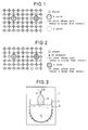
- Fig. 1 is a schematic view illustrating a Si single crystal solely doped with P
- Fig. 2 is a schematic view illustrating a Si single crystal double-doped with P and B
- Fig. 3 is a schematic view for explaining a pulling method of producing a double-doped Si crystal from a Si melt
- Fig. 4 is a schematic view for explaining a vapor deposition method of producing a Si crystal double-doped with P and B
- Fig. 5 is a schematic view for explaining a selective diffusion method of producing a Si crystal double-doped with P and B
- Fig.6 is a schematic view illustrating a section of a Si single crystal substrate which has a region double-doped with P and B by diffusion
-
- When Si is solely doped with P or B according to a conventional method, concentration of the dopant is approximately 1019/cm3 at most. Even if much more amount of P or B is added to Si, number of carriers can not be increased due to increase of lattice defects That is, since an substitutional atomic position of Si is not replaced by P or B, a trap center is realized due to appearance of atomic vacancy of Si and an atom is inserted to an interstitial position. As a result, resistivity of the doped Si is not lowered any more.
- When Si is double-doped with P and B, concentration of the dopants can be increased to a level exceeding 1020/cm3. The inventor suppose the effect of the double-doping on increase of concentration as follows:
- When Si is double-doped with P (whose ionic radius is larger than Si) and B (whose ionic radius is smaller than Si), a strain energy of Si is relaxed so that Si can be heavily-doped up to high concentration without accumulation of strain. Consequently, the Si single crystal is heavily-doped up to high concentration without any lattice default.
- In addition, the element X serving as a donor and the element Y serving as an acceptor are charged at positive (+) and negative (-) potentials; respectively, so as to enable coexistence of n-type and p-type dopants. A Coulomb force between the n-type and p-type dopants reduces an electrostatic energy, resulting in stabilization of crystallographic structure.
- Double-doping with P and B at an atomic ratio of (1+α):1 under such condition effectively promotes growth of a n-type Si crystal having low resistivity and including electrons as a carrier. While, double-doping with P and B at an atomic ratio of 1:(1+α) promotes growth of a p-type Si crystal including holes as a carrier. Herein, the Si crystal can be heavily-doped up to high concentration exceeding 1020/cm3, although compared concentration is approximately 1019/cm3 or so at most by conventional sole P or B doping.
- The Si crystal heavily-doped in this way exhibits metallic property but not dielectric property. That is, the heavily-doped Si has a sufficiently low resistivity in an order of 10-2-10-5Ω-cm, so that the heavily-doped Si itself is useful as a wiring material for electrically connecting various semiconductor devices without necessity of a thin metal film such as Au or Al.
- A Si material was inserted in a
crucible 2 located in avacuum chamber 1. The Si material was heated up to 1550°C by a high-frequency induction heater 3 and melted to prepare a Si melt 4. The Si melt 4 was mixed with P and B. Addition amount of P was adjusted at 6 × 10²⁰/cm3, 1 × 10²²/cm3, 2 × 10²²/cm3 and 6 × 10²²/cm3, while an amount of B was controlled to a half of an equivalency to the corresponding amount of P. - After the Si melt 4 became uniform, a
seed crystal 5 was brought in contact with the Si melt 4. Theseed crystal 5 was rotated and gradually lifted up at a speed of 1 cm/hour to grow a Sisingle crystal 6 from the Si melt 4. - Each Si single crystal obtained in this way was tested to detect a number of carriers. The results are shown in Table 1. It is noted from Table 1 that the Si crystal double-doped with P and B has a number of carriers 100-times or much higher than that of a solely P-doped Si crystal without addition of B. Such heavy doping is the typical effect of the double-doping with P and B and enables production of n-type metallic Si having low resistivity.
EFFECTS OF DOUBLE-DOPING IN A PULLING METHOD AMOUNT OF P ADDED TO SIILICON MELT (/cm3) NUMBER OF CARRIERS IN DOPED SILICON CRYSTAL (/cm3) DOUBLE-DOPING WITH P AND B (P:B=2:1) SOLE P-DOPING 6×10²⁰ 2.1×10²⁰ 3.1×10¹⁸ 1×10²² 2.8×10²¹ 2.6×10¹⁹ 2×10²² 3.5×10²¹ 3.4×10¹⁹ 6×10²² 1.1×10²² 4.2×10¹⁹ - A molecular beam epitaxy device was used in Example 2 for double-doping a Si layer, which was grown up according to a vapor-phase epitaxy method, with P and B.
A Si substrate 12 was set in avacuum chamber 11 held in an evacuated atmosphere at a degree of vacuum of 1.3×10⁻⁸ Pa as shown in Fig. 4. An atomic Si beam activated by a high-frequency induction heater 13 was supplied to the vacuum chamber at a partial pressure of 1.3×10⁻⁴ Pa, so as to epitaxially grow aSi crystal 14 on theSi substrate 12. At the same time, aB beam 17 and aP beam 18 each activated byheaters vacuum chamber 11. - Each
Si crystal 14 obtained in this way was tested to detect a concentration of carriers. The results are shown in Table 2. It is noted from Table 2 that the Si crystal double-doped with P and B had a concentration of carriers 100-500 times higher compared with that of solely P-doped Si without B-doping. These results also show the effect of the double-doping on increase of concentration and production of n-type metallic Si having low resistivity.EFFECTS OF DOUBLE-DOPING IN A VAPOR-PHASE DEPOSITION AMOUNT OF P ADDED TO SILICON (/cm3) CONCENTRATION OR CARRIERS IN DOPED SILICON (/cm3) DOUBLE-DOPING WITH P AND B (P:B=3:1) SOLE P- DOPING 1 × 10²¹ 5.0 × 10²⁰ 4.2 × 10¹⁸ 1.5 × 10²² 3.0 × 10²¹ 5.6 × 10¹⁹ 1.5×10²³ 3.1 × 10²² 6.2 × 10¹⁹ - P serving as a
donor 22 together with B serving as anacceptor 23 was vapor deposited on a Sisinge crystal substrate 21, as shown in Fig. 4. Thereafter, thesubstrate 21 was annealed at 1200°C in a furnace to diffuse P and B into the Si crystal. Due to diffusion of P and B, aregion 24 double-doped with P and B was formed in the Sisingle crystal substrate 21, as shown in Fig. 5. - Doping rates of P and B were varied by changing an annealing time. Each doped Si was tested to research the effect of the double-doping on a number of carriers. The results are shown in Table 3, compared with solely P-doped Si without vapor deposition of B. It is noted from Table 3 that the Si crystal double-doped with P and B had a number of carriers 100-350 times higher in comparison with thesolely P-doped Si. These results are also the evidence that the double-doping with P and B remarkably increases number of carriers and enables production of n-type metallic Si having sufficiently low resistivity.
EFFECTS OF DOUBLE DOPING WITH P AND B IN SELECTIVE DIFFUSION ON NUMBER OF CARRIERS ANNEALING TIME (hrs.) NUMBER OF CARRIERS IN DOPED SILICON CRYSTAL (/cm3) DOUBLE-DOPING WITH P AND B (P:B=2:1) SOLE P-DOPING 0.5 6.1 × 10¹⁹ 4.3 × 10¹⁸ 5 2.1 × 10²² 5.8 × 10¹⁹ - According to the present invention as aforementioned, a Si crystal is double-doped with at least one element X whose ionic radius is larger than Si together with at least one element Y selected from B, Al, Ga and In whose ionic radius is smaller than Si at an atomic ratio of 1:(1+α) or (1+α):1 with the provision of α being a value of 1-5. The double doping remarkably increases the number of carriers up to 1020-1022/cm3, although a number of carriers in a doped Si according to a conventional method is approximately 1019/cm3 or so at most. The Si heavily-doped in this way has sufficiently low resistivity as compared with conventional n-type or p-type Si. Due to the low resistivity, the double-doped Si itself is useful as a wiring material without deposition of a thin metal film such as Au or Al, and semiconductor devices can be integrated with extremely high density.
Claims (4)
- A method of producing a heavily-doped Si having low resistivity, which comprises the steps of:adding at least one element X selected from P, As, Sb whose ionic radius is larger than Si together with at least one element Y selected from B, Al, Ga and In whose ionic radius is smaller than Si at an atomic ratio of X:Y=1:(1+α) or X:Y=(1+α):1 with the provision of α being a value of 1 - 5 to a Si growing atmosphere so as to heavily-dope Si with the elements X and Y at a high concentration of 1020 - 1022/cm3.
- The method defined by Claim 1, using a Si melt to which the elements X and Y are added at an atomic ratio of X:Y=1:(1+α) or X:Y=(1+α):1, and a heavily-doped Si crystal is pulled up from said Si melt.
- The method defined by Claim 1, wherein the element X whose ionic radius is larger than Si and the element Y whose ionic radius is smaller than Si are simultaneously supplied as molecular beams together with at least one Si beam to a Si growing atmosphere during epitaxial growth of metallic Si from a vapor phase so as to double- dope an epitaxially growing Si crystal with the elements X and Y.
- The method defined by Claim 1, wherein the element X whose ionic radius is larger than Si and the element Y whose ionic radius is smaller than Si are vapor deposited on a Si single crystal substrate and then diffused by annealing so as to form a region where Si is double-doped with the elements X and Y.
Applications Claiming Priority (3)
| Application Number | Priority Date | Filing Date | Title |
|---|---|---|---|
| JP223304/97 | 1997-08-20 | ||
| JP22330497 | 1997-08-20 | ||
| JP22330497A JP3525141B2 (en) | 1997-08-20 | 1997-08-20 | Method for producing n-type or p-type metal silicon having low resistivity |
Publications (3)
| Publication Number | Publication Date |
|---|---|
| EP0903429A2 EP0903429A2 (en) | 1999-03-24 |
| EP0903429A3 EP0903429A3 (en) | 2000-08-09 |
| EP0903429B1 true EP0903429B1 (en) | 2004-01-07 |
Family
ID=16796058
Family Applications (1)
| Application Number | Title | Priority Date | Filing Date |
|---|---|---|---|
| EP98115709A Expired - Lifetime EP0903429B1 (en) | 1997-08-20 | 1998-08-20 | Process for producing heavily doped silicon |
Country Status (4)
| Country | Link |
|---|---|
| US (1) | US6013129A (en) |
| EP (1) | EP0903429B1 (en) |
| JP (1) | JP3525141B2 (en) |
| DE (1) | DE69820940T2 (en) |
Families Citing this family (7)
| Publication number | Priority date | Publication date | Assignee | Title |
|---|---|---|---|---|
| US7132091B2 (en) | 2001-09-28 | 2006-11-07 | Memc Electronic Materials, Inc. | Single crystal silicon ingot having a high arsenic concentration |
| US6888170B2 (en) * | 2002-03-15 | 2005-05-03 | Cornell Research Foundation, Inc. | Highly doped III-nitride semiconductors |
| US6953740B2 (en) * | 2002-03-15 | 2005-10-11 | Cornell Research Foundation, Inc. | Highly doped III-nitride semiconductors |
| JP4207577B2 (en) * | 2003-01-17 | 2009-01-14 | 信越半導体株式会社 | Method for producing P-doped silicon single crystal |
| DE102004004555A1 (en) * | 2004-01-29 | 2005-08-18 | Siltronic Ag | Process for the production of highly doped semiconductor wafers and dislocation-free, highly doped semiconductor wafers |
| US7922817B2 (en) | 2008-04-24 | 2011-04-12 | Memc Electronic Materials, Inc. | Method and device for feeding arsenic dopant into a silicon crystal growing apparatus |
| JP7151096B2 (en) * | 2018-02-21 | 2022-10-12 | 株式会社デンソー | Piezoelectric film, manufacturing method thereof, piezoelectric film laminate, manufacturing method thereof |
Family Cites Families (7)
| Publication number | Priority date | Publication date | Assignee | Title |
|---|---|---|---|---|
| US3485684A (en) * | 1967-03-30 | 1969-12-23 | Trw Semiconductors Inc | Dislocation enhancement control of silicon by introduction of large diameter atomic metals |
| GB1426511A (en) * | 1973-02-02 | 1976-03-03 | Handotai Kenkyu Shinkokai | Method for producing a semiconductor device having a very small deviation in lattice constant |
| US4631234A (en) * | 1985-09-13 | 1986-12-23 | Texas Instruments Incorporated | Germanium hardened silicon substrate |
| JPH0717477B2 (en) * | 1989-03-15 | 1995-03-01 | シャープ株式会社 | Epitaxial growth method of compound semiconductor |
| EP0460937B1 (en) * | 1990-06-05 | 1994-10-19 | Matsushita Electric Industrial Co., Ltd. | Method for fabricating a semiconductor laser device |
| US5169798A (en) * | 1990-06-28 | 1992-12-08 | At&T Bell Laboratories | Forming a semiconductor layer using molecular beam epitaxy |
| US5553566A (en) * | 1995-06-22 | 1996-09-10 | Motorola Inc. | Method of eliminating dislocations and lowering lattice strain for highly doped N+ substrates |
-
1997
- 1997-08-20 JP JP22330497A patent/JP3525141B2/en not_active Expired - Fee Related
-
1998
- 1998-08-19 US US09/136,554 patent/US6013129A/en not_active Expired - Fee Related
- 1998-08-20 EP EP98115709A patent/EP0903429B1/en not_active Expired - Lifetime
- 1998-08-20 DE DE69820940T patent/DE69820940T2/en not_active Expired - Lifetime
Also Published As
| Publication number | Publication date |
|---|---|
| DE69820940D1 (en) | 2004-02-12 |
| JPH1167768A (en) | 1999-03-09 |
| JP3525141B2 (en) | 2004-05-10 |
| US6013129A (en) | 2000-01-11 |
| EP0903429A3 (en) | 2000-08-09 |
| DE69820940T2 (en) | 2004-11-04 |
| EP0903429A2 (en) | 1999-03-24 |
Similar Documents
| Publication | Publication Date | Title |
|---|---|---|
| Becker et al. | Acceptor dopants in silicon molecular‐beam epitaxy | |
| US4962051A (en) | Method of forming a defect-free semiconductor layer on insulator | |
| JP4117914B2 (en) | Process for controlling dopant diffusion in a semiconductor layer and semiconductor layer formed thereby | |
| US6896731B1 (en) | P-type single crystal zinc-oxide having low resistivity and method for preparation thereof | |
| JPH04230037A (en) | Vapor application method of n-type silicon layer, npn transistor | |
| US4699688A (en) | Method of epitaxially growing gallium arsenide on silicon | |
| JPH0714764A (en) | Thin film polycrystalline silicon and manufacturing method thereof | |
| US5553566A (en) | Method of eliminating dislocations and lowering lattice strain for highly doped N+ substrates | |
| US4859626A (en) | Method of forming thin epitaxial layers using multistep growth for autodoping control | |
| EP0334682B1 (en) | Method for forming P-type germanium layer on a gallium arsenide body | |
| EP0903429B1 (en) | Process for producing heavily doped silicon | |
| US8329532B2 (en) | Process for the simultaneous deposition of crystalline and amorphous layers with doping | |
| US5549749A (en) | Substrate with a compound semiconductor surface layer and method for preparing the same | |
| JP2911694B2 (en) | Semiconductor substrate and method of manufacturing the same | |
| JPH02260628A (en) | Manufacture of semiconductor device | |
| JPWO2002099890A1 (en) | Semiconductor layer and method for forming the same, and semiconductor device and method for manufacturing the same | |
| EP0779652A2 (en) | Method for making a heterojunction bipolar transistor | |
| EP0196245B1 (en) | Compound semiconductor layer having high carrier concentration and method of forming same | |
| JP2848404B2 (en) | Method for forming group III-V compound semiconductor layer | |
| US5250147A (en) | Method of producing a layer system and a layer system as produced thereby | |
| US6838359B2 (en) | Suppression of n-type autodoping in low-temperature Si and SiGe epitaxy | |
| JP2555885B2 (en) | Germanium / gallium arsenide junction manufacturing method | |
| JPH0714840B2 (en) | Epitaxial film growth method | |
| KR960004904B1 (en) | Growing method for ga-as on the porous silicon substrate | |
| JP3149457B2 (en) | Silicon germanium film, method for manufacturing silicon germanium film, and semiconductor device manufactured using silicon germanium film |
Legal Events
| Date | Code | Title | Description |
|---|---|---|---|
| PUAI | Public reference made under article 153(3) epc to a published international application that has entered the european phase |
Free format text: ORIGINAL CODE: 0009012 |
|
| AK | Designated contracting states |
Kind code of ref document: A2 Designated state(s): DE FR GB |
|
| AX | Request for extension of the european patent |
Free format text: AL;LT;LV;MK;RO;SI |
|
| PUAL | Search report despatched |
Free format text: ORIGINAL CODE: 0009013 |
|
| RIC1 | Information provided on ipc code assigned before grant |
Free format text: 7C 30B 29/06 A, 7C 30B 23/02 B, 7C 30B 15/00 B, 7C 30B 25/02 B, 7H 01L 29/167 B |
|
| AK | Designated contracting states |
Kind code of ref document: A3 Designated state(s): AT BE CH CY DE DK ES FI FR GB GR IE IT LI LU MC NL PT SE |
|
| AX | Request for extension of the european patent |
Free format text: AL;LT;LV;MK;RO;SI |
|
| 17P | Request for examination filed |
Effective date: 20000914 |
|
| AKX | Designation fees paid |
Free format text: DE FR GB |
|
| 17Q | First examination report despatched |
Effective date: 20020429 |
|
| GRAP | Despatch of communication of intention to grant a patent |
Free format text: ORIGINAL CODE: EPIDOSNIGR1 |
|
| GRAS | Grant fee paid |
Free format text: ORIGINAL CODE: EPIDOSNIGR3 |
|
| GRAA | (expected) grant |
Free format text: ORIGINAL CODE: 0009210 |
|
| AK | Designated contracting states |
Kind code of ref document: B1 Designated state(s): DE FR GB |
|
| REG | Reference to a national code |
Ref country code: GB Ref legal event code: FG4D |
|
| REF | Corresponds to: |
Ref document number: 69820940 Country of ref document: DE Date of ref document: 20040212 Kind code of ref document: P |
|
| ET | Fr: translation filed | ||
| PLBE | No opposition filed within time limit |
Free format text: ORIGINAL CODE: 0009261 |
|
| STAA | Information on the status of an ep patent application or granted ep patent |
Free format text: STATUS: NO OPPOSITION FILED WITHIN TIME LIMIT |
|
| 26N | No opposition filed |
Effective date: 20041008 |
|
| PGFP | Annual fee paid to national office [announced via postgrant information from national office to epo] |
Ref country code: FR Payment date: 20100901 Year of fee payment: 13 Ref country code: DE Payment date: 20100823 Year of fee payment: 13 |
|
| PGFP | Annual fee paid to national office [announced via postgrant information from national office to epo] |
Ref country code: GB Payment date: 20100819 Year of fee payment: 13 |
|
| GBPC | Gb: european patent ceased through non-payment of renewal fee |
Effective date: 20110820 |
|
| REG | Reference to a national code |
Ref country code: FR Ref legal event code: ST Effective date: 20120430 |
|
| REG | Reference to a national code |
Ref country code: DE Ref legal event code: R119 Ref document number: 69820940 Country of ref document: DE Effective date: 20120301 |
|
| PG25 | Lapsed in a contracting state [announced via postgrant information from national office to epo] |
Ref country code: GB Free format text: LAPSE BECAUSE OF NON-PAYMENT OF DUE FEES Effective date: 20110820 Ref country code: FR Free format text: LAPSE BECAUSE OF NON-PAYMENT OF DUE FEES Effective date: 20110831 |
|
| PG25 | Lapsed in a contracting state [announced via postgrant information from national office to epo] |
Ref country code: DE Free format text: LAPSE BECAUSE OF NON-PAYMENT OF DUE FEES Effective date: 20120301 |