EP0902979B1 - Thyristor a protection du/dt integree - Google Patents
Thyristor a protection du/dt integree Download PDFInfo
- Publication number
- EP0902979B1 EP0902979B1 EP97923788A EP97923788A EP0902979B1 EP 0902979 B1 EP0902979 B1 EP 0902979B1 EP 97923788 A EP97923788 A EP 97923788A EP 97923788 A EP97923788 A EP 97923788A EP 0902979 B1 EP0902979 B1 EP 0902979B1
- Authority
- EP
- European Patent Office
- Prior art keywords
- base
- thyristor
- emitter
- cathode side
- auxiliary
- Prior art date
- Legal status (The legal status is an assumption and is not a legal conclusion. Google has not performed a legal analysis and makes no representation as to the accuracy of the status listed.)
- Expired - Lifetime
Links
- 239000004065 semiconductor Substances 0.000 claims description 10
- 238000007747 plating Methods 0.000 claims 3
- 239000000126 substance Substances 0.000 claims 1
- 238000001465 metallisation Methods 0.000 description 6
- 238000000034 method Methods 0.000 description 5
- 239000002019 doping agent Substances 0.000 description 3
- XUIMIQQOPSSXEZ-UHFFFAOYSA-N Silicon Chemical compound [Si] XUIMIQQOPSSXEZ-UHFFFAOYSA-N 0.000 description 2
- 230000015556 catabolic process Effects 0.000 description 2
- 230000001419 dependent effect Effects 0.000 description 2
- 238000006073 displacement reaction Methods 0.000 description 2
- 238000004519 manufacturing process Methods 0.000 description 2
- 230000003287 optical effect Effects 0.000 description 2
- 230000035945 sensitivity Effects 0.000 description 2
- 229910052710 silicon Inorganic materials 0.000 description 2
- 239000010703 silicon Substances 0.000 description 2
- 230000002411 adverse Effects 0.000 description 1
- 238000010276 construction Methods 0.000 description 1
- 230000006378 damage Effects 0.000 description 1
- 238000011161 development Methods 0.000 description 1
- 230000018109 developmental process Effects 0.000 description 1
- 238000010304 firing Methods 0.000 description 1
- PNDPGZBMCMUPRI-UHFFFAOYSA-N iodine Chemical group II PNDPGZBMCMUPRI-UHFFFAOYSA-N 0.000 description 1
- 230000002045 lasting effect Effects 0.000 description 1
- 239000002184 metal Substances 0.000 description 1
- 230000005855 radiation Effects 0.000 description 1
- 230000002441 reversible effect Effects 0.000 description 1
- 230000003068 static effect Effects 0.000 description 1
- 230000002123 temporal effect Effects 0.000 description 1
- 230000001960 triggered effect Effects 0.000 description 1
Images

Classifications
-
- H—ELECTRICITY
- H10—SEMICONDUCTOR DEVICES; ELECTRIC SOLID-STATE DEVICES NOT OTHERWISE PROVIDED FOR
- H10D—INORGANIC ELECTRIC SEMICONDUCTOR DEVICES
- H10D18/00—Thyristors
- H10D18/211—Thyristors having built-in localised breakdown or breakover regions, e.g. self-protected against destructive spontaneous firing
-
- H—ELECTRICITY
- H10—SEMICONDUCTOR DEVICES; ELECTRIC SOLID-STATE DEVICES NOT OTHERWISE PROVIDED FOR
- H10D—INORGANIC ELECTRIC SEMICONDUCTOR DEVICES
- H10D18/00—Thyristors
- H10D18/221—Thyristors having amplifying gate structures, e.g. cascade configurations
-
- H—ELECTRICITY
- H10—SEMICONDUCTOR DEVICES; ELECTRIC SOLID-STATE DEVICES NOT OTHERWISE PROVIDED FOR
- H10D—INORGANIC ELECTRIC SEMICONDUCTOR DEVICES
- H10D62/00—Semiconductor bodies, or regions thereof, of devices having potential barriers
- H10D62/10—Shapes, relative sizes or dispositions of the regions of the semiconductor bodies; Shapes of the semiconductor bodies
- H10D62/17—Semiconductor regions connected to electrodes not carrying current to be rectified, amplified or switched, e.g. channel regions
- H10D62/192—Base regions of thyristors
- H10D62/206—Cathode base regions of thyristors
Definitions
- the dU / dt strength of a thyristor can be significantly improved, since a large part of the capacitive displacement current I d in the semiconductor body no longer flows via the cathode-side pn junction, but from the base directly to the cathode.
- the critical value of the voltage gradient corresponding to built-thyristors is typically several 1000 V / ⁇ s.
- a thyristor is known, in whose cathode-side base a resistance zone and a p-doped zone adjoining it are arranged between an n-doped auxiliary emitter and the anode-side base.
- the EP 0 062 100 A2 shows a thyristor with a firing stage structure comprising two auxiliary emitters.
- the auxiliary emitter closest to the ignition electrode extends deeply into the cathode-side base, so that its resistance increases below this auxiliary emitter.
- a thyristor which has portions with increased doping which adjoin laterally portions of lower doping.
- the portions with lower doping have in a projection perpendicular to the cathode plane on rectangular projection surfaces.
- a thyristor having a main thyristor section a pilot thyristor and an ignition stage structure is described.
- the doping of the cathode-side base with respect to the doping of the cathode-side base in the region of the main thyristor is reduced.
- the WO 86/00469 A shows a main thyristor whose cathode-side base has a resistance zone which extends over the entire thickness of the cathode-side base to the surface of the semiconductor body.
- the subject of the invention is a particularly light-ignitable and BOD-protected thyristor with integrated dU / dt protection.
- the thyristor should be constructed so that it ignites uncontrolled in the region of the cathode surface or the edge termination in the case of too large a dU / dt load in the tilting direction, a thyristor having the features specified in claim 1 has this property.
- the dependent claims relate to advantageous embodiments and refinements of the thyristor.
- the ignition behavior of a thyristor is decisively influenced by the sheet resistance of the cathode-side base.
- the invention uses this property in order to displace the ignition process caused by an excessive dU / dt load purposefully into the central region of the thyristor. Since the volume affected by the ignition is always within the range bounded by the first auxiliary thyristor, the plasma, as in a controlled ignition, can propagate over a large area and uniformly in the radial direction without the current density reaching critical values.
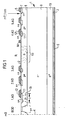
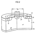
- FIG. 1 shown in cross-section, equipped with a BOD (b reac o comparable d iode) structure light triggered thyristor has a rotationally symmetrical structure with respect to the perpendicular to the two major surfaces 2/3 of the semiconductor body 1 axis 4. While the upper major surface 2 of the disc-shaped semiconductor body 1 carries the edge extending, provided with so-called emitter short-circuit cathode metallization 5, its back major surface 3 is completely coated with a serving as an anode metallization 6.
- the existing of silicon semiconductor body 1 has a plurality of differently doped, each separated by space charge zones regions 7 -10.
- the AG ( A mplifying G ate) designated, arranged radially inside the cathode metallization 5 auxiliary thyristors serve as driver stages for the main thyristor. They each have an embedded in the cathode-side base 8, n + -doped auxiliary emitter 11/11 'and a both the auxiliary emitter 11/11' and the base 8 contacting metallization 12/12 'on. Which is doped on the n + region 11/11 'extending metallization 12/12' has suppressed the function of a short-circuiting emitter, / dt unwanted ignition of the auxiliary thyristor of each of large voltage gradients dU effective.
- a zone 13 of the cathode-side base 8 surrounding the inner three auxiliary thyristors (1st-3rd AG) in an annular manner the dopant concentration is reduced compared to the laterally adjacent regions.
- This annular zone 13 acts as a resistor R, which limits the ignition current flowing radially outwards in the base 8 to a predetermined maximum value and thus reduces the load on the structure during the switch-on process (see, for example, [2] or [3]).
- the electrons injected by the adjoining auxiliary emitter 11 'into the cathode-side base 8 can recombine, so that the resistor R undergoes no modulation when the thyristor is turned on.
- the sheet resistance R ⁇ of the approximately 200-600 ⁇ m wide annular zone 15 is typically R ⁇ ⁇ 2000-4000 ⁇ ⁇ . It is thus 10-20 times larger than the sheet resistance of the adjacent base region (R ⁇ (p + ) ⁇ 200 - 400 ⁇ ⁇ ).
- the invention is of course not limited to the embodiment described above.
Landscapes
- Thyristors (AREA)
Claims (6)
- Thyristor comprenanta) successivement, dans un corps semi-conducteur (1), un émetteur côté cathode (7) d'un premier type de conductivité, une base côté cathode (8) d'un deuxième type de conductivité, une base côté anode (9) dudit premier type de conductivité ainsi qu'un émetteur côté anode (10) dudit deuxième type de conductivité,b) un revêtement métallique cathodique (5) appliqué sur ledit émetteur côté cathode (7) ainsi qu'un revêtement métallique anodique (6) appliqué sur ledit émetteur côté anode (10),c) plusieurs thyristors auxiliaires annulaires (1. - 5. AG) disposés de façon concentrique qui comprennent chacun un émetteur auxiliaire (11, 11') qui est enrobé dans ladite base côté cathode (8) et qui est formé par une zone annulaire du premier type de conductivité et est disposé de manière que ledit émetteur côté cathode (7) est situé à l'extérieur de la zone entourée par ledit émetteur auxiliaire (11, 11'),d) un revêtement métallique (12) des émetteurs (11), qui contacte ladite base côté cathode (8),e) une zone annulaire (15) qui est disposée au-dessous de l'émetteur auxiliaire situé le plus à l'intérieur (11), entre ledit émetteur situé le plus à l'intérieur (11) et ladite base côté anode (9), mais non pas au-dessous de l'un des autres émetteurs auxiliaires, et qui est formée par une zone annulaire dans la base côté cathode (8), dans laquelle la concentration du dopage est réduite par rapport aux zones de la base côté cathode (8) qui se joignent latéralement, etf) une structure d'amorçage disposée dans la zone centrale dudit corps semi-conducteur (1) et commandée optiquement ou électriquement.
- Thyristor selon la revendication 1, dans lequel les concentrations du dopant sont choisies de telle manière que la résistance série électrique dans la zone annulaire (15) est plus importante d'un facteur 5 à 20 que la résistance série électrique des zones de la base côté cathode qui se joignent latéralement.
- Thyristor selon la revendication 1 ou 2, dans lequel ladite zone annulaire (15) présente une largeur comprise entre 200 µm et 600 µm.
- Thyristor selon l'une quelconque des revendications 1 à 3, dans lequel une zone centrale du corps semi-conducteur (1), qui est entourée par ladite zone annulaire (15), Intègre une structure BOD.
- Thyristor selon la revendication 4, dans lequel ladite structure BOD est constituée par- ledit émetteur auxiliaire (11),- ladite zone annulaire (15),- une zone annulaire qui est contiguë, dans la couche de la base côté cathode, vers le centre, à ladite zone annulaire (15) et qui est fortement dopée du deuxième type de conductivité,- une autre zone annulaire d'épaisseur plus faible qui est contiguë, vers le centre, à cette zone annulaire et qui est, elle aussi, fortement dopée du deuxième type de conductivité et est contiguë également à ladite base côté anode (9), et par- une zone centrale qui est contiguë à cette autre zone annulaire et à ladite base côté anode et qui est fortement dopée du deuxième type de conductivité et présente à peu près l'épaisseur de ladite base côté cathode.
- Thyristor selon la revendication 1, dans lequel, entre deux thyristors auxiliaires, une autre zone annulaire (13) de résistance électrique élevée est localisée dans ladite base côté cathode (8).
Applications Claiming Priority (5)
| Application Number | Priority Date | Filing Date | Title |
|---|---|---|---|
| DE19620184 | 1996-05-20 | ||
| DE19620184 | 1996-05-20 | ||
| DE19650763 | 1996-12-06 | ||
| DE19650763 | 1996-12-06 | ||
| PCT/DE1997/000927 WO1997044827A1 (fr) | 1996-05-20 | 1997-05-07 | Thyristor a protection du/dt integree |
Publications (2)
| Publication Number | Publication Date |
|---|---|
| EP0902979A1 EP0902979A1 (fr) | 1999-03-24 |
| EP0902979B1 true EP0902979B1 (fr) | 2010-07-14 |
Family
ID=26025838
Family Applications (1)
| Application Number | Title | Priority Date | Filing Date |
|---|---|---|---|
| EP97923788A Expired - Lifetime EP0902979B1 (fr) | 1996-05-20 | 1997-05-07 | Thyristor a protection du/dt integree |
Country Status (4)
| Country | Link |
|---|---|
| US (1) | US6066864A (fr) |
| EP (1) | EP0902979B1 (fr) |
| DE (1) | DE59713039D1 (fr) |
| WO (1) | WO1997044827A1 (fr) |
Families Citing this family (9)
| Publication number | Priority date | Publication date | Assignee | Title |
|---|---|---|---|---|
| EP0931351B1 (fr) * | 1996-09-30 | 2004-01-28 | EUPEC Europäische Gesellschaft für Leistungshalbleiter mbH & Co. KG | Thyristor avec zone de claquage |
| DE19826022C1 (de) * | 1998-06-10 | 1999-06-17 | Siemens Ag | Vorrichtung und Verfahren zur Ansteuerung von Thyristoren |
| US6811680B2 (en) | 2001-03-14 | 2004-11-02 | Applied Materials Inc. | Planarization of substrates using electrochemical mechanical polishing |
| DE10135984B4 (de) * | 2001-07-24 | 2005-04-21 | eupec Europäische Gesellschaft für Leistungshalbleiter mbH & Co. KG | Anordnung mit einem lichtzündbaren Halbleiterbauelement und einem Teil zur Lichtdurchführung |
| DE10135983B4 (de) * | 2001-07-24 | 2005-05-04 | eupec Europäische Gesellschaft für Leistungshalbleiter mbH & Co. KG | Lichtzündbarer Thyristor |
| US6770911B2 (en) * | 2001-09-12 | 2004-08-03 | Cree, Inc. | Large area silicon carbide devices |
| DE10231199A1 (de) * | 2002-07-10 | 2004-02-05 | eupec Europäische Gesellschaft für Leistungshalbleiter mbH | Halbleiterbauelement |
| DE102004062183B3 (de) * | 2004-12-23 | 2006-06-08 | eupec Europäische Gesellschaft für Leistungshalbleiter mbH | Thyristoranordnung mit integriertem Schutzwiderstand und Verfahren zu deren Herstellung |
| DE102011002479A1 (de) * | 2011-01-05 | 2012-07-05 | Infineon Technologies Bipolar Gmbh & Co. Kg | Verfahren zur Herstellung eines Halbleiterbauelements mit integriertem Lateralwiderstand |
Family Cites Families (10)
| Publication number | Priority date | Publication date | Assignee | Title |
|---|---|---|---|---|
| FR2377095A1 (fr) * | 1977-01-10 | 1978-08-04 | Alsthom Atlantique | Thyristor a amplificateur de declenchement et a ouverture commandee par la gachette |
| DE3112941A1 (de) * | 1981-03-31 | 1982-10-07 | Siemens AG, 1000 Berlin und 8000 München | Thyristor mit innerer stromverstaerkung und verfahren zu seinem betrieb |
| JPS59220970A (ja) * | 1983-05-31 | 1984-12-12 | Meidensha Electric Mfg Co Ltd | 増幅ゲ−ト構造のgto |
| US4908687A (en) * | 1984-06-29 | 1990-03-13 | General Electric Company | Controlled turn-on thyristor |
| WO1986000469A1 (fr) * | 1984-06-29 | 1986-01-16 | General Electric Company | Thyristor a mise sous tension regulee |
| EP0219995B1 (fr) * | 1985-09-30 | 1994-03-02 | Kabushiki Kaisha Toshiba | Thyristor à commande d'extinction comportant des transistors d'allumage/extinction indépendants |
| US5204273A (en) * | 1990-08-20 | 1993-04-20 | Siemens Aktiengesellschaft | Method for the manufacturing of a thyristor with defined lateral resistor |
| DE4215378C1 (de) * | 1992-05-11 | 1993-09-30 | Siemens Ag | Thyristor mit Durchbruchbereich |
| FR2708811B1 (fr) * | 1993-08-06 | 1995-10-20 | Sgs Thomson Microelectronics | Thyristor à amplification de gachette à courant de maintien accru. |
| JPH07122728A (ja) * | 1993-10-25 | 1995-05-12 | Toshiba Corp | 半導体装置 |
-
1997
- 1997-05-07 US US09/194,178 patent/US6066864A/en not_active Expired - Lifetime
- 1997-05-07 WO PCT/DE1997/000927 patent/WO1997044827A1/fr not_active Ceased
- 1997-05-07 EP EP97923788A patent/EP0902979B1/fr not_active Expired - Lifetime
- 1997-05-07 DE DE59713039T patent/DE59713039D1/de not_active Expired - Lifetime
Also Published As
| Publication number | Publication date |
|---|---|
| DE59713039D1 (de) | 2010-08-26 |
| US6066864A (en) | 2000-05-23 |
| EP0902979A1 (fr) | 1999-03-24 |
| WO1997044827A1 (fr) | 1997-11-27 |
Similar Documents
| Publication | Publication Date | Title |
|---|---|---|
| EP0200863B1 (fr) | Dispositif à semi-conducteur comportant des structures de type thyristor et diode | |
| EP0360036B1 (fr) | Jonction pn plane à tenue en tension élévée | |
| DE2625917B2 (de) | Halbleiteranordnung | |
| DE2107564B2 (de) | Durch Lichteinfall steuerbarer Thyristor | |
| DE2716874C2 (de) | Thyristor | |
| EP0902979B1 (fr) | Thyristor a protection du/dt integree | |
| EP0572826B1 (fr) | Thyristor avec région de claquage | |
| EP0931351B1 (fr) | Thyristor avec zone de claquage | |
| DE1207502B (de) | Flaechenhaftes Halbleiterbauelement mit mindestens einem sperrenden pn-UEbergang und Verfahren zum Herstellen | |
| DE3240564A1 (de) | Steuerbares halbleiterschaltelement | |
| EP0327901B1 (fr) | Thyristor GTO de forte puissance et méthode de fabrication | |
| DE3328231C2 (fr) | ||
| DE3787848T2 (de) | Halbleiterdiode. | |
| EP0144876A2 (fr) | Dispositif à semi-conducteurs | |
| EP0062099B1 (fr) | Thyristor et procédé pour son fonctionnement | |
| EP0430133B1 (fr) | Dispositif semi-conducteur de puissance comportant des courts-circuits d'émetteur | |
| DE19650762A1 (de) | Thyristor mit Durchbruchbereich | |
| DE102019124695A1 (de) | Kurzschluss-Halbleiterbauelement und Verfahren zu dessen Betrieb | |
| EP0970525B1 (fr) | Thyristor asymetrique | |
| EP0651445A2 (fr) | Thyristor bloquable | |
| EP0062100B1 (fr) | Thyristor avec amplification de courant interne et procédé pour son fonctionnement | |
| CH679962A5 (fr) | ||
| DE2406866C3 (de) | Steuerbarer Halbleitergleichrichter | |
| DE2607194A1 (de) | Halbleiteranordnung | |
| EP0389942B1 (fr) | Dispositif semi-conducteur à tension de blocage élevée |
Legal Events
| Date | Code | Title | Description |
|---|---|---|---|
| PUAI | Public reference made under article 153(3) epc to a published international application that has entered the european phase |
Free format text: ORIGINAL CODE: 0009012 |
|
| 17P | Request for examination filed |
Effective date: 19981105 |
|
| AK | Designated contracting states |
Kind code of ref document: A1 Designated state(s): DE FR GB |
|
| RAP1 | Party data changed (applicant data changed or rights of an application transferred) |
Owner name: INFINEON TECHNOLOGIES AG |
|
| 17Q | First examination report despatched |
Effective date: 20070827 |
|
| GRAP | Despatch of communication of intention to grant a patent |
Free format text: ORIGINAL CODE: EPIDOSNIGR1 |
|
| GRAJ | Information related to disapproval of communication of intention to grant by the applicant or resumption of examination proceedings by the epo deleted |
Free format text: ORIGINAL CODE: EPIDOSDIGR1 |
|
| GRAP | Despatch of communication of intention to grant a patent |
Free format text: ORIGINAL CODE: EPIDOSNIGR1 |
|
| GRAS | Grant fee paid |
Free format text: ORIGINAL CODE: EPIDOSNIGR3 |
|
| RAP1 | Party data changed (applicant data changed or rights of an application transferred) |
Owner name: INFINEON TECHNOLOGIES AG |
|
| GRAA | (expected) grant |
Free format text: ORIGINAL CODE: 0009210 |
|
| AK | Designated contracting states |
Kind code of ref document: B1 Designated state(s): DE FR GB |
|
| REG | Reference to a national code |
Ref country code: GB Ref legal event code: FG4D Free format text: NOT ENGLISH |
|
| REF | Corresponds to: |
Ref document number: 59713039 Country of ref document: DE Date of ref document: 20100826 Kind code of ref document: P |
|
| PLBE | No opposition filed within time limit |
Free format text: ORIGINAL CODE: 0009261 |
|
| STAA | Information on the status of an ep patent application or granted ep patent |
Free format text: STATUS: NO OPPOSITION FILED WITHIN TIME LIMIT |
|
| 26N | No opposition filed |
Effective date: 20110415 |
|
| REG | Reference to a national code |
Ref country code: DE Ref legal event code: R097 Ref document number: 59713039 Country of ref document: DE Effective date: 20110415 |
|
| REG | Reference to a national code |
Ref country code: FR Ref legal event code: ST Effective date: 20120131 |
|
| PG25 | Lapsed in a contracting state [announced via postgrant information from national office to epo] |
Ref country code: FR Free format text: LAPSE BECAUSE OF NON-PAYMENT OF DUE FEES Effective date: 20110531 |
|
| PGFP | Annual fee paid to national office [announced via postgrant information from national office to epo] |
Ref country code: GB Payment date: 20160523 Year of fee payment: 20 Ref country code: DE Payment date: 20160525 Year of fee payment: 20 |
|
| REG | Reference to a national code |
Ref country code: DE Ref legal event code: R082 Ref document number: 59713039 Country of ref document: DE Representative=s name: LOHMANNS, BERNARD, DIPL.-PHYS., DE |
|
| REG | Reference to a national code |
Ref country code: DE Ref legal event code: R071 Ref document number: 59713039 Country of ref document: DE |
|
| REG | Reference to a national code |
Ref country code: GB Ref legal event code: PE20 Expiry date: 20170506 |
|
| PG25 | Lapsed in a contracting state [announced via postgrant information from national office to epo] |
Ref country code: GB Free format text: LAPSE BECAUSE OF EXPIRATION OF PROTECTION Effective date: 20170506 |