EP0902909B1 - Interference filter based on porous silicon - Google Patents
Interference filter based on porous silicon Download PDFInfo
- Publication number
- EP0902909B1 EP0902909B1 EP97925897A EP97925897A EP0902909B1 EP 0902909 B1 EP0902909 B1 EP 0902909B1 EP 97925897 A EP97925897 A EP 97925897A EP 97925897 A EP97925897 A EP 97925897A EP 0902909 B1 EP0902909 B1 EP 0902909B1
- Authority
- EP
- European Patent Office
- Prior art keywords
- interference filter
- refractive index
- substance
- interference
- porous
- Prior art date
- Legal status (The legal status is an assumption and is not a legal conclusion. Google has not performed a legal analysis and makes no representation as to the accuracy of the status listed.)
- Expired - Lifetime
Links
Images


Classifications
-
- G—PHYSICS
- G02—OPTICS
- G02F—OPTICAL DEVICES OR ARRANGEMENTS FOR THE CONTROL OF LIGHT BY MODIFICATION OF THE OPTICAL PROPERTIES OF THE MEDIA OF THE ELEMENTS INVOLVED THEREIN; NON-LINEAR OPTICS; FREQUENCY-CHANGING OF LIGHT; OPTICAL LOGIC ELEMENTS; OPTICAL ANALOGUE/DIGITAL CONVERTERS
- G02F1/00—Devices or arrangements for the control of the intensity, colour, phase, polarisation or direction of light arriving from an independent light source, e.g. switching, gating or modulating; Non-linear optics
- G02F1/01—Devices or arrangements for the control of the intensity, colour, phase, polarisation or direction of light arriving from an independent light source, e.g. switching, gating or modulating; Non-linear optics for the control of the intensity, phase, polarisation or colour
- G02F1/21—Devices or arrangements for the control of the intensity, colour, phase, polarisation or direction of light arriving from an independent light source, e.g. switching, gating or modulating; Non-linear optics for the control of the intensity, phase, polarisation or colour by interference
-
- G—PHYSICS
- G02—OPTICS
- G02F—OPTICAL DEVICES OR ARRANGEMENTS FOR THE CONTROL OF LIGHT BY MODIFICATION OF THE OPTICAL PROPERTIES OF THE MEDIA OF THE ELEMENTS INVOLVED THEREIN; NON-LINEAR OPTICS; FREQUENCY-CHANGING OF LIGHT; OPTICAL LOGIC ELEMENTS; OPTICAL ANALOGUE/DIGITAL CONVERTERS
- G02F1/00—Devices or arrangements for the control of the intensity, colour, phase, polarisation or direction of light arriving from an independent light source, e.g. switching, gating or modulating; Non-linear optics
- G02F1/01—Devices or arrangements for the control of the intensity, colour, phase, polarisation or direction of light arriving from an independent light source, e.g. switching, gating or modulating; Non-linear optics for the control of the intensity, phase, polarisation or colour
- G02F1/13—Devices or arrangements for the control of the intensity, colour, phase, polarisation or direction of light arriving from an independent light source, e.g. switching, gating or modulating; Non-linear optics for the control of the intensity, phase, polarisation or colour based on liquid crystals, e.g. single liquid crystal display cells
- G02F1/133—Constructional arrangements; Operation of liquid crystal cells; Circuit arrangements
- G02F1/1333—Constructional arrangements; Manufacturing methods
- G02F1/1334—Constructional arrangements; Manufacturing methods based on polymer dispersed liquid crystals, e.g. microencapsulated liquid crystals
Definitions
- the invention relates to an interference filter or a Component with interference filter function on the basis of porous material, especially silicon according to the Preamble of claim 1.
- WO 91/10926 relates to a composite volume-phase hologram and other optical holographic Elements, and in particular the provision of holographic Elements with a discontinuous Distribution of a separate phase, which is a liquid crystal contains.
- the composite optical holographic Elements show a different Refractive effect as a function of external stimuli such as an applied electric field.
- US 4,970,129 relates to volume phase holograms and others holographic elements, and in particular the Production of volume phase holograms and others holographic elements characterized are that they are microscopic areas of a material with a refractive index different from the holographic Stripes (fringes) differs.
- the holographic Elements can have an increased diffractive effect and / or have other desirable properties.
- the pores in the PS are filled with a substance under the influence of an electrical Field can change its refractive index.
- liquid crystals come as a suitable Material considered, the birefringent properties own and their refractive index through reorientation of the molecular chains in an electric field or is adjustable.
- an interference filter for example a computer chip be formed from a particular matrix-shaped arrangement of several reflection filters, preferably for the three primary colors red, green and Blue exists. Each of these can be activated individually be trained.
- a chip can be a projection display, for example for imaging Devices such as a monitor or TV set become.
- porous silicon consists of a spongy one Framework of silicon crystallites, which of Pores.
- the size of the crystallites and the Pores vary depending on the doping of the starting substrate in the range of preferably 2 nanometers to 2 micrometers.
- the PS appears for the Light as a homogeneous material ("effective medium") and its properties are indicated by specifying an effective one Refractive index described, which of the Refractive index of the silicon crystallites and the volume fraction the pores (porosity) depends.
- the invention is not limited to PS as a porous material. Rather, there are others porous materials conceivable with suitable material.
- the filter structure according to the invention is shown in FIG shown.
- volume fraction i.e. porosity
- the refractive index n of the silicon skeleton z. B. is changeable by oxidation.
- the end result can then be a layer system made of porous glass (SiO 2 ).
- the refractive index of the filled substance corresponds to that of the silicon or SiO 2 crystallites at at least one specific voltage (e.g. when voltage is applied)
- the effective refractive index of a layer is no longer dependent on the volume fraction of the substance.
- the layer system loses its filtering effect since each individual layer now has the same refractive index.
- the low oscillations are caused by interference caused over the entire sample thickness.
- the refractive index of the substance located in the pores changes towards large values and deviates from that of the silicon or SiO 2 crystallites. Due to the different volume fractions of the substance in porous layers with different porosity, there is an overall greater change in the refractive index for those layers with high porosity. The course of the refractive index over the depth of the layer which results in the voltage-free case consequently leads to the further reflection spectrum shown in the lower part of FIG. A very high reflectivity results for a certain wavelength, which is predetermined, for example, by the choice of the production parameters of the layer system.
- the example shown here therefore shows in tensionless case a green color impression of the Layer system, while when the voltage is applied Black layer system appears.
- Such electrically changeable Interference filters can e.g. in reflection displays or also for color selective detectors with, higher spectral sensitivity are used.
- FIG. 4 shows the structure of a reflection display shown schematically, which is for example by assembling several interference filter functions in matrix form on a single substrate gives:
- White light turns on the electrically changeable Interference filter given.
- the individual can choose Filter according to the invention controlled separately or together be so that on the projection screen formed from the sum of the individual reflections Point of light is displayed in the desired color.
- a matrix of such filter layers thus forms a reflection display, which colored pictures on the Projection screen.
- the imaging reflection points can be done in this way the color changed or adjusted and thus the desired one Pixel can be obtained. In this way can be formed from many such pixels Overall picture such as a screen in reflection be preserved.
- porous SiGe or GaAs or other materials for forming the invention imaginable there are, for example, porous SiGe or GaAs or other materials for forming the invention imaginable.
Landscapes
- Physics & Mathematics (AREA)
- Nonlinear Science (AREA)
- General Physics & Mathematics (AREA)
- Optics & Photonics (AREA)
- Liquid Crystal (AREA)
Description
Die Erfindung betrifft einen Interferenzfilter oder ein
Bauelement mit Interferenzfilterfunktion auf der Basis
von porösem Material, insbesondere Silicium gemäß dem
Oberbegriff des Anspruchs 1.The invention relates to an interference filter or a
Component with interference filter function on the basis
of porous material, especially silicon according to the
Preamble of
WO 91/10926 betrifft ein zusammengesetztes Volumen-Phasen-Hologramm und andere optische holographische Elemente, und insbesondere die Bereitstellung von holographischen Elementen mit einer diskontinuierlichen Verteilung einer getrennten Phase, die einen Flüssigkristall enthält. Die zusammengesetzten optischen holographischen Elemente zeigen eine unterschiedliche Brechungswirkung als Funktion externer Anregungen wie einem angelegten elektrischen Feld.WO 91/10926 relates to a composite volume-phase hologram and other optical holographic Elements, and in particular the provision of holographic Elements with a discontinuous Distribution of a separate phase, which is a liquid crystal contains. The composite optical holographic Elements show a different Refractive effect as a function of external stimuli such as an applied electric field.
US 4,970,129 betrifft Volumen-Phasen-Hologramme und andere holographischen Elemente, und insbesondere die Herstellung von Volumen-Phasen-Hologrammen und anderen holographischen Elementen, die dadurch gekennzeichnet sind, daß sie mikroskopische Bereiche eines Materials mit einem Brechungsindex besitzen, der sich von dem holographischer Streifen (fringes) unterscheidet. Die holographischen Elemente können eine erhöhte Beugungswirkung und/oder andere wünschenswerte Eigenschaften aufweisen.US 4,970,129 relates to volume phase holograms and others holographic elements, and in particular the Production of volume phase holograms and others holographic elements characterized are that they are microscopic areas of a material with a refractive index different from the holographic Stripes (fringes) differs. The holographic Elements can have an increased diffractive effect and / or have other desirable properties.
Als Stand der Technik ist weiterhin aus M.G. Berger et al., Mat. Res. Soc. Symp. Proc. 358, 327 (1995) oder DE-OS 43 19 413 die Eignung des porösen Siliciums (PS) bekannt, Schichtsysteme mit nahezu beliebigem Aufbau durch einen elektrochemischen Prozeß zur Realisierung von Interferenzfiltern herzustellen. Mit Hilfe derartiger Interferenzfilter lassen sich sowohl Reflexionsals auch Transmissionsfilter für Lichtwellenlängen im gesamten sichtbaren, aber auch infraroten oder ultravioletten Spektralbereich herstellen. Dabei ist es möglich, poröses Silicium nicht nur großflächig, sondern mit Hilfe der aus der Halbleitertechnik bekannten Photolithographie auch auf lateralen Dimensionen von wenigen Mikrometern herzustellen, sodaß auf vergleichweise kleiner Fläche unterschiedliche Interferenzfilter gebildet werden. As state of the art, M.G. Berger et al., Mat. Res. Soc. Symp. Proc. 358, 327 (1995) or DE-OS 43 19 413 the suitability of the porous silicon (PS) known, layer systems with almost any structure through an electrochemical process for realization of interference filters. With the help of such Interference filters can be both reflection and also transmission filters for light wavelengths in total visible, but also infrared or ultraviolet Establish spectral range. It is possible porous silicon not only over a large area, but also with the help of photolithography known from semiconductor technology even on lateral dimensions of a few Manufacture micrometers so that on comparative different interference filters are formed in a small area become.
Bei geeigneter Wahl der Herstellungsparameter lassen sich Interferenzfilter mit erwünschter Reflexions- oder Transmissionseigenschaft herstellen, wie aus M.G. Berger et al., in Optical Interference Coatings, Florin Abeles ed., Proc. SPIE 2253, 865 (1994) bekannt. Es wurde z. B. ein sogenannter Bragg-Reflektor hergestellt, der einerseits für bestimmte Farben im sichtbaren Spektralbereich ein sehr hohes Reflexionsvermögen aufweist, andererseits andere Farben praktisch nicht reflektiert.Leave with a suitable choice of manufacturing parameters interference filter with the desired reflection or Establish transmission property, as from M.G. Berger et al. in Optical Interference Coatings, Florin Abeles ed., Proc. SPIE 2253, 865 (1994). It z. B. a so-called Bragg reflector is produced, on the one hand for certain colors in the visible Spectral range a very high reflectivity on the other hand practically not other colors reflected.
Nachteilig bei den bekannten Bauelementen mit Interferenzfilterfunktion ist die Festlegung dieser Funktion durch die Herstellungsrandbedingungen.A disadvantage of the known components with an interference filter function is the definition of this function by the manufacturing constraints.
Es ist deshalb Aufgabe der Erfindung ein Bauelement mit Interferenzfilterfunktion bzw. ein Interferenzfilter auf der Basis eines porösen Materials insbesondere Siliciums zu schaffen, deren Reflexions- und/oder Transmissionseigenschaft auch nach Herstellung des Bauelements gezielt einstellbar oder veränderbar ist.It is therefore an object of the invention to provide a component Interference filter function or an interference filter based on a porous material, especially silicon to create their reflection and / or transmission property even after the component has been manufactured is specifically adjustable or changeable.
Die Aufgabe wird gelöst durch ein Bauelement mit Interferenzfilterfunktion
gemäß der Gesamtheit der Merkmale
nach Anspruch 1. Weitere zweckmäßige oder vorteilhafte
Ausführungsformen finden sich in den auf diesen Anspruch
rückbezogenen Unteransprüchen. The object is achieved by a component with an interference filter function
according to all the features
according to
Es wurde erkannt, die Poren des PS mit geeignetem Material aufzufüllen und durch Anlegen einer elektrischen Spannung an dieses Material gezielt die Reflektions und / oder Transmissionseigenschaften einstellbar veränderbar auszubilden.It was recognized the pores of the PS with suitable material fill up and by applying an electrical Tension on this material targeted the reflection and / or transmission properties adjustable adjustable train.
Im einzelnen erfolgt das Auffüllen der Poren im PS mit einer Substanz, die unter dem Einfluß eines elektrischen Feldes ihren Brechungsindex verändern kann. Hierbei kommen vorzugsweise Flüssigkristalle als geeignetes Material in Betracht, die doppelbrechende Eigenschaften besitzen und deren Brechungsindex durch Umorientierung der Molekülketten in einem elektrischen Feld veränderoder einstellbar ist.In particular, the pores in the PS are filled with a substance under the influence of an electrical Field can change its refractive index. in this connection preferably liquid crystals come as a suitable Material considered, the birefringent properties own and their refractive index through reorientation of the molecular chains in an electric field or is adjustable.
Mit Hilfe des erfindungsgemäßen Bauelements, insbesondere als Interferenzfilter, kann zum Beispiel ein Computerchip gebildet werden, der aus einer insbesondere matrixförmigen Anordnung mehrerer Reflexionsfilter, vorzugsweise für die drei Grundfarben Rot, Grün und Blau, besteht. Dabei können diese jeweils einzeln aktivierbar ausgebildet sein. Mit Hilfe eines solchen Chips kann ein Projektionsdisplay, beispielsweise für bildgebende Geräte, wie z.B. ein Monitor oder TV-Gerät, gebildet werden.With the aid of the component according to the invention, in particular as an interference filter, for example a computer chip be formed from a particular matrix-shaped arrangement of several reflection filters, preferably for the three primary colors red, green and Blue exists. Each of these can be activated individually be trained. With the help of such a chip can be a projection display, for example for imaging Devices such as a monitor or TV set become.
Im einzelnen besteht poröses Silicium aus einem schwammartigen Gerüst von Silicium-Kristalliten, welches von Poren durchzogen ist. Die Größe der Kristallite und der Poren variiert je nach Dotierung des Ausgangssubstrats im Bereich von vorzugsweise 2 Nanometer bis 2 Mikrometer.In particular, porous silicon consists of a spongy one Framework of silicon crystallites, which of Pores. The size of the crystallites and the Pores vary depending on the doping of the starting substrate in the range of preferably 2 nanometers to 2 micrometers.
Falls die Wellenlänge des Lichtes sehr viel größer als die Strukturen im PS ist, erscheint das PS für das Licht als homogenes Material ("effektives Medium") und seine Eigenschaften werden durch die Angabe eines effektiven Brechungsindexes beschrieben, welcher von den Brechungsindizes der Silicium-Kristallite und dem Volumenanteil der Poren (Porosität) abhängt.If the wavelength of light is much larger than the structures in the PS is, the PS appears for the Light as a homogeneous material ("effective medium") and its properties are indicated by specifying an effective one Refractive index described, which of the Refractive index of the silicon crystallites and the volume fraction the pores (porosity) depends.
Wird bei dem elektrochemischen Ätzprozeß nicht nur eine Schicht mit einer bestimmten Porosität hergestellt, sondern stattdessen ein Schichtsystem, welches aus einer Abfolge einzelner Schichten mit unterschiedlicher Porosität besteht, so werden durch die unterschiedlichen effektiven Brechungsindizes der Einzelschichten Interferenzeffekte im Schichtsystem hervorgerufen. Auf diese Weise lassen sich z.B. Filter herstellen, die, wenn sie mit einer weißen Lichtquelle beleuchtet werden, nur eine Wellenlänge, d.h. Farbe reflektieren. Nach der Herstellung des Schichsystems ist diese Farbe nicht mehr veränderlich.Not only one in the electrochemical etching process Layer with a certain porosity, but instead a layer system, which consists of a Sequence of individual layers with different ones Porosity exists because of the different effective refractive indices of the individual layers Interference effects caused in the layer system. On in this way e.g. Make filters that when illuminated with a white light source, only one wavelength, i.e. Reflect color. This is the color after the layering system is made no longer changeable.
Es wurde nun erkannt, die Poren des PS mit einer Substanz aufzufüllen, die ihren Brechungsindex durch das Anlegen einer elektrischen Spannung bzw. unter dem Einfluß eines elektrischen Feldes verändert (z.B. Flüssigkristalle). Die Änderung des Brechungsindexes der Substanz unter dem Einfluß eines elektrischen Feldes kann dabei sowohl kontinuierlich als auch sprungweise erfolgen. Ebenso ist es möglich, daß sich - wie im Falle von Flüssigkristallen - der Brechungsindex durch die Ausrichtung von Molekülketten nur für bestimmte Ausbreitungsrichtungen des Lichtes ändert.It has now been recognized the pores of the PS with a substance to fill up their refractive index by that Applying an electrical voltage or under the influence an electrical field (e.g. liquid crystals). The change in the refractive index of the substance under the influence of an electric field take place both continuously and step by step. It is also possible that - as in the case of Liquid crystals - the refractive index due to the alignment of molecular chains only for certain directions of propagation of the light changes.
Im übrigen beschränkt sich die Erfindung nicht auf PS als porenbehaftetes Material. Es sind vielmehr auch andere porenbehaftete Materialien vorstellbar, die mit geeignetem Material aufgefüllt werden.Otherwise, the invention is not limited to PS as a porous material. Rather, there are others porous materials conceivable with suitable material.
Die Erfindung ist im weiteren an Hand von Figuren und Ausführungsbeispielen näher erläutert. Es zeigen:
- Fig. 1:
- erfindungsgemäßes Bauelement mit einer eine Interferenzfilterfunktion aufweisenden Schichtenfolge;
- Fig. 2:
- Tiefenabhängigkeit des Brechungsindexes n für
eine Schichtenfolge gemäß
Figur 1 mit und ohne angelegter Spannung; - Fig. 3:
- Wellenzahlabhängigkeit der Reflektivität der erfindungsgemäßen die Filterstruktur bildende Schichtenfolge;
- Fig. 4:
- mehrere erfindungsgemäße Interferenzfilter zur Bildung eines Reflektionsdisplays.
- Fig. 1:
- Component according to the invention with a layer sequence having an interference filter function;
- Fig. 2:
- Depth dependence of the refractive index n for a layer sequence according to FIG. 1 with and without applied voltage;
- Fig. 3:
- Wave number dependence of the reflectivity of the layer sequence according to the invention forming the filter structure;
- Fig. 4:
- several interference filters according to the invention to form a reflection display.
In der Figur 1 ist die erfindungsgemäße Filterstruktur dargestellt.The filter structure according to the invention is shown in FIG shown.
Im einzelnen ist dazu eine Schichtenfolge mit aufeinanderfolgenden Schichten hergestellt. Auf einem Substrat ist eine Anti-Reflxionsschicht gebildet. Darauf findet sich das mit angelegter elektrischer Spannung steuerbare Schichtensystem aus PS mit unterschiedlicher Porosität in den einzelnen Schichten. Die Zahl der PS-Schichten kann mehr oder weniger groß gewählt werden zum Beispiel 60.In detail there is a layer sequence with successive Layers. On a substrate an anti-reflection layer is formed. Find on it that can be controlled with the applied electrical voltage Layer system made of PS with different porosity in the individual layers. The number of PS shifts can be chosen more or less large for example 60.
Die elektrisch erzeugte Änderung des Brechungsindexes der Substanz bewirkt je nach deren jeweiligen Volumenanteil (d. h. Porosität) eine mehr oder weniger starke Änderung des effektiven Brechungsindexes der porösen Schicht. Um eine möglichst große Änderung des Reflexions- bzw. Transmissionsvermögens des gesamten Schichtsystems zu erreichen, bietet sich eine spezielle Wahl der Brechungsindizes vom porösen Silicium-Skelett und der in die Poren eingefüllten Substanz an.The electrically generated change in the refractive index the substance causes depending on their respective volume fraction (i.e. porosity) a more or less strong Change the effective refractive index of the porous Layer. In order to change the reflection or transmittance of the entire layer system to achieve, there is a special choice the refractive indices of the porous silicon skeleton and of the substance filled in the pores.
Hierzu ist festzuhalten, daß der Brechungsindex n des Silicium-Skeletts z. B. durch eine Oxidation veränderbar ist. Das Endergebnis kann dann ein Schichtsystem aus porösem Glas (SiO2) sein.It should be noted that the refractive index n of the silicon skeleton z. B. is changeable by oxidation. The end result can then be a layer system made of porous glass (SiO 2 ).
Entspricht der Brechungsindex der eingefüllten Substanz bei wenigstens einer bestimmten Spannung (z. B. bei angelegter Spannung) demjenigen der Silicium- oder SiO2-Kristallite, so ist der effektive Brechungsindex einer Schicht nicht mehr von dem Volumenanteil der Substanz abhängig. Folglich verliert das Schichtsystem seine filternde Wirkung, da nun jede Einzelschicht denselben Brechungsindex aufweist.If the refractive index of the filled substance corresponds to that of the silicon or SiO 2 crystallites at at least one specific voltage (e.g. when voltage is applied), the effective refractive index of a layer is no longer dependent on the volume fraction of the substance. As a result, the layer system loses its filtering effect since each individual layer now has the same refractive index.
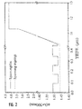
In der Figur 2 ist der Verlauf des Brechungsindexes über die Schichttiefe für einen solchen Fall eingezeichnet. Dabei stelle der gestrichelte Verlauf den Fall angelegter Spannung dar.The course of the refractive index is over in FIG the layer depth is drawn for such a case. The dashed line represents the case Tension.
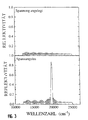
Für die in dem Beispiel von Figur 2 angenommenen Werte ergibt sich dann das oben in Figur 3 dargestellte Reflexionsspektrum. Es weist eine über den gesamten dargestellten Spektralbereich niedrige Reflektivität auf. For the values assumed in the example in FIG. 2 The reflection spectrum shown above in FIG. 3 then results. It has one shown across the entire Spectral range low reflectivity.
Die geringen Oszillationen werden durch Interferenzen über die gesamte Probendicke verursacht.The low oscillations are caused by interference caused over the entire sample thickness.
Im spannungslosen Fall, dargestellt durch die durchgezogene Linie in Figur 2, ändert sich der Brechungsindex der in den Poren befindlichen Substanz zu größen Werten hin und weicht von demjenigen der Silicium- bzw. SiO2-Kristallite ab. Durch die unterschiedlichen Volumenanteile der Substanz in porösen Schichten mit unterschiedlicher Porosität ergibt sich insgesamt eine stärkere Änderung des Brechungsindexes für diejenigen Schichten mit hoher Porosität. Der sich im spannungslosen Fall ergebende Verlauf des Brechungsindexes über die Schichttiefe führt demzufolge zu dem im unteren Teil von Figur 3 gezeigten weiteren Reflexionsspektrum. Für eine bestimmte Wellenlänge, die zum Beispiel durch die Wahl der Herstellungsparameter des Schichtsystems vorgegeben ist, ergibt sich eine sehr hohe Reflektivität.In the de-energized case, represented by the solid line in FIG. 2, the refractive index of the substance located in the pores changes towards large values and deviates from that of the silicon or SiO 2 crystallites. Due to the different volume fractions of the substance in porous layers with different porosity, there is an overall greater change in the refractive index for those layers with high porosity. The course of the refractive index over the depth of the layer which results in the voltage-free case consequently leads to the further reflection spectrum shown in the lower part of FIG. A very high reflectivity results for a certain wavelength, which is predetermined, for example, by the choice of the production parameters of the layer system.
In dem hier gezeigten Beispiel zeigt sich daher im spannungslosen Fall ein grüner Farbeindruck des Schichtsystems, während bei angelegter Spannung das Schichtsystem schwarz erscheint. Derart elektrisch veränderliche Interferenzfilter können z.B. in Reflexionsdisplays oder auch für farbselektive Detektoren mit,hoher spektraler Empfindlichkeit zum Einsatz kommen. The example shown here therefore shows in tensionless case a green color impression of the Layer system, while when the voltage is applied Black layer system appears. Such electrically changeable Interference filters can e.g. in reflection displays or also for color selective detectors with, higher spectral sensitivity are used.
In der Figur 4 ist der Aufbau eines Reflektionsdisplays schematisch dargestellt, welches sich beispielsweise durch Zusammenbau mehrerer Interferenzfilterfunktionen in Matrixform auf einem einzelnen Substrat ergibt:FIG. 4 shows the structure of a reflection display shown schematically, which is for example by assembling several interference filter functions in matrix form on a single substrate gives:
Weisses Licht wird auf die elektrisch veränderlichen Interferenzfilter gegeben. Wahlweise können die einzelnen erfindungsgemäßen Filter getrennt oder zusammen angesteuert werden, so daß auf dem Projektionsschirm ein aus der Summe der einzelnen Reflexionen gebildeter Lichtpunkt in der gewünschten Farbe dargestellt wird. Eine Matrix von solchen Filterschichten bildet somit ein Reflexionsdisplay, welches farbige Bilder auf dem Projektionsschirm darstellen kann. Durch Ansteuerung der bildgebenden Reflektionspunkte kann auf diese Weise die Farbe verändert oder eingestellt und somit der erwünschte Bildpunkt erhalten werden. Auf diese Weise kann ein aus vielen solchen Bildpunkten zu bildendes Gesamtbild wie zum Beispiel ein Bildschirm in Reflektion erhalten werden.White light turns on the electrically changeable Interference filter given. The individual can choose Filter according to the invention controlled separately or together be so that on the projection screen formed from the sum of the individual reflections Point of light is displayed in the desired color. A matrix of such filter layers thus forms a reflection display, which colored pictures on the Projection screen. By control The imaging reflection points can be done in this way the color changed or adjusted and thus the desired one Pixel can be obtained. In this way can be formed from many such pixels Overall picture such as a screen in reflection be preserved.
Außer PS sind zum Beispiel auch poröses SiGe oder GaAs oder andere Materialien zur Ausbildung der Erfindung vorstellbar.In addition to PS, there are, for example, porous SiGe or GaAs or other materials for forming the invention imaginable.
Claims (4)
- An interference filter or a component with an interference filter function, comprising at least one layer of porous material, wherein at least part of the pores or all the pores of the porous material are filled with a substance, the refractive index of which can be set to a defined value by an external effect,
characterised in that
the refractive index of the substance can be set to the value of the refractive index of the porous material and the porous material consists of porous Si, SiO2, SiGe or GaAs. - An interference filter or a component with an interference filter function according to claim 1,
characterised in that
the refractive index of the substance can be varied or adjusted by an electric voltage or by an electric current. - An interference filter or a component with an interference filter function according to claim 1,
characterised in that
the refractive index of the substance can be varied or adjusted by a change in temperature. - A matrix arrangement, particularly on a single substrate, comprising a multiplicity of interference filters or of components which perform interference filter functions according to one or more of the preceding claims, for forming a reflection display.
Applications Claiming Priority (3)
| Application Number | Priority Date | Filing Date | Title |
|---|---|---|---|
| DE19622748 | 1996-06-05 | ||
| DE1996122748 DE19622748A1 (en) | 1996-06-05 | 1996-06-05 | Interference filter based on porous silicon |
| PCT/DE1997/001117 WO1997046908A1 (en) | 1996-06-05 | 1997-05-30 | Interference filter based on porous silicon |
Publications (2)
| Publication Number | Publication Date |
|---|---|
| EP0902909A1 EP0902909A1 (en) | 1999-03-24 |
| EP0902909B1 true EP0902909B1 (en) | 2002-10-02 |
Family
ID=7796317
Family Applications (1)
| Application Number | Title | Priority Date | Filing Date |
|---|---|---|---|
| EP97925897A Expired - Lifetime EP0902909B1 (en) | 1996-06-05 | 1997-05-30 | Interference filter based on porous silicon |
Country Status (4)
| Country | Link |
|---|---|
| EP (1) | EP0902909B1 (en) |
| JP (1) | JP2000514568A (en) |
| DE (2) | DE19622748A1 (en) |
| WO (1) | WO1997046908A1 (en) |
Families Citing this family (46)
| Publication number | Priority date | Publication date | Assignee | Title |
|---|---|---|---|---|
| US6674562B1 (en) | 1994-05-05 | 2004-01-06 | Iridigm Display Corporation | Interferometric modulation of radiation |
| US7907319B2 (en) | 1995-11-06 | 2011-03-15 | Qualcomm Mems Technologies, Inc. | Method and device for modulating light with optical compensation |
| DE19757321A1 (en) * | 1997-12-23 | 1999-07-01 | Forschungszentrum Juelich Gmbh | Optical component with a surface provided for optical applications |
| WO1999052006A2 (en) | 1998-04-08 | 1999-10-14 | Etalon, Inc. | Interferometric modulation of radiation |
| US8928967B2 (en) | 1998-04-08 | 2015-01-06 | Qualcomm Mems Technologies, Inc. | Method and device for modulating light |
| WO2000045202A1 (en) * | 1999-02-01 | 2000-08-03 | Mcnc | A tunable electrooptic interference filter and method of manufacturing same |
| DE19921190A1 (en) * | 1999-05-07 | 2000-11-16 | Forschungszentrum Juelich Gmbh | Process for manufacturing an element with porosidized material |
| TWI289708B (en) | 2002-12-25 | 2007-11-11 | Qualcomm Mems Technologies Inc | Optical interference type color display |
| US7342705B2 (en) | 2004-02-03 | 2008-03-11 | Idc, Llc | Spatial light modulator with integrated optical compensation structure |
| RU2379725C2 (en) * | 2004-02-03 | 2010-01-20 | АйДиСи, ЭлЭлСи | Spatial light modulator with integrated optical compensation structure |
| US7706050B2 (en) | 2004-03-05 | 2010-04-27 | Qualcomm Mems Technologies, Inc. | Integrated modulator illumination |
| US7855824B2 (en) | 2004-03-06 | 2010-12-21 | Qualcomm Mems Technologies, Inc. | Method and system for color optimization in a display |
| US7508571B2 (en) | 2004-09-27 | 2009-03-24 | Idc, Llc | Optical films for controlling angular characteristics of displays |
| US7349141B2 (en) | 2004-09-27 | 2008-03-25 | Idc, Llc | Method and post structures for interferometric modulation |
| US8362987B2 (en) | 2004-09-27 | 2013-01-29 | Qualcomm Mems Technologies, Inc. | Method and device for manipulating color in a display |
| US7355780B2 (en) | 2004-09-27 | 2008-04-08 | Idc, Llc | System and method of illuminating interferometric modulators using backlighting |
| US7710636B2 (en) | 2004-09-27 | 2010-05-04 | Qualcomm Mems Technologies, Inc. | Systems and methods using interferometric optical modulators and diffusers |
| US7813026B2 (en) | 2004-09-27 | 2010-10-12 | Qualcomm Mems Technologies, Inc. | System and method of reducing color shift in a display |
| US7561323B2 (en) | 2004-09-27 | 2009-07-14 | Idc, Llc | Optical films for directing light towards active areas of displays |
| US7807488B2 (en) | 2004-09-27 | 2010-10-05 | Qualcomm Mems Technologies, Inc. | Display element having filter material diffused in a substrate of the display element |
| US7928928B2 (en) | 2004-09-27 | 2011-04-19 | Qualcomm Mems Technologies, Inc. | Apparatus and method for reducing perceived color shift |
| US7898521B2 (en) | 2004-09-27 | 2011-03-01 | Qualcomm Mems Technologies, Inc. | Device and method for wavelength filtering |
| US7630123B2 (en) | 2004-09-27 | 2009-12-08 | Qualcomm Mems Technologies, Inc. | Method and device for compensating for color shift as a function of angle of view |
| US7710632B2 (en) | 2004-09-27 | 2010-05-04 | Qualcomm Mems Technologies, Inc. | Display device having an array of spatial light modulators with integrated color filters |
| US7911428B2 (en) | 2004-09-27 | 2011-03-22 | Qualcomm Mems Technologies, Inc. | Method and device for manipulating color in a display |
| US7916980B2 (en) | 2006-01-13 | 2011-03-29 | Qualcomm Mems Technologies, Inc. | Interconnect structure for MEMS device |
| US7603001B2 (en) | 2006-02-17 | 2009-10-13 | Qualcomm Mems Technologies, Inc. | Method and apparatus for providing back-lighting in an interferometric modulator display device |
| US8004743B2 (en) | 2006-04-21 | 2011-08-23 | Qualcomm Mems Technologies, Inc. | Method and apparatus for providing brightness control in an interferometric modulator (IMOD) display |
| US7845841B2 (en) | 2006-08-28 | 2010-12-07 | Qualcomm Mems Technologies, Inc. | Angle sweeping holographic illuminator |
| US7855827B2 (en) | 2006-10-06 | 2010-12-21 | Qualcomm Mems Technologies, Inc. | Internal optical isolation structure for integrated front or back lighting |
| CN101600901A (en) | 2006-10-06 | 2009-12-09 | 高通Mems科技公司 | Optical loss structure integrated in illumination device of display |
| WO2008045311A2 (en) | 2006-10-06 | 2008-04-17 | Qualcomm Mems Technologies, Inc. | Illumination device with built-in light coupler |
| WO2008045207A2 (en) | 2006-10-06 | 2008-04-17 | Qualcomm Mems Technologies, Inc. | Light guide |
| EP1946162A2 (en) | 2006-10-10 | 2008-07-23 | Qualcomm Mems Technologies, Inc | Display device with diffractive optics |
| US7864395B2 (en) | 2006-10-27 | 2011-01-04 | Qualcomm Mems Technologies, Inc. | Light guide including optical scattering elements and a method of manufacture |
| US7777954B2 (en) | 2007-01-30 | 2010-08-17 | Qualcomm Mems Technologies, Inc. | Systems and methods of providing a light guiding layer |
| US7733439B2 (en) | 2007-04-30 | 2010-06-08 | Qualcomm Mems Technologies, Inc. | Dual film light guide for illuminating displays |
| US8068710B2 (en) | 2007-12-07 | 2011-11-29 | Qualcomm Mems Technologies, Inc. | Decoupled holographic film and diffuser |
| JP2011507306A (en) | 2007-12-17 | 2011-03-03 | クォルコム・メムズ・テクノロジーズ・インコーポレーテッド | Photovoltaic device with interference backside mask |
| WO2009102733A2 (en) | 2008-02-12 | 2009-08-20 | Qualcomm Mems Technologies, Inc. | Integrated front light diffuser for reflective displays |
| WO2009102731A2 (en) | 2008-02-12 | 2009-08-20 | Qualcomm Mems Technologies, Inc. | Devices and methods for enhancing brightness of displays using angle conversion layers |
| US8049951B2 (en) | 2008-04-15 | 2011-11-01 | Qualcomm Mems Technologies, Inc. | Light with bi-directional propagation |
| JP5484567B2 (en) | 2009-05-29 | 2014-05-07 | クォルコム・メムズ・テクノロジーズ・インコーポレーテッド | Illumination device and method of processing an illumination device |
| US8848294B2 (en) | 2010-05-20 | 2014-09-30 | Qualcomm Mems Technologies, Inc. | Method and structure capable of changing color saturation |
| US8670171B2 (en) | 2010-10-18 | 2014-03-11 | Qualcomm Mems Technologies, Inc. | Display having an embedded microlens array |
| US8902484B2 (en) | 2010-12-15 | 2014-12-02 | Qualcomm Mems Technologies, Inc. | Holographic brightness enhancement film |
Citations (2)
| Publication number | Priority date | Publication date | Assignee | Title |
|---|---|---|---|---|
| US4970129A (en) * | 1986-12-19 | 1990-11-13 | Polaroid Corporation | Holograms |
| WO1991010926A1 (en) * | 1990-01-12 | 1991-07-25 | Polaroid Corporation | Volume phase hologram with liquid crystal in microvoids between fringes |
Family Cites Families (7)
| Publication number | Priority date | Publication date | Assignee | Title |
|---|---|---|---|---|
| US4411495A (en) * | 1981-04-15 | 1983-10-25 | Bell Telephone Laboratories, Incorporated | Refractive index switchable display cell |
| US4828888A (en) * | 1987-04-10 | 1989-05-09 | Hoecast Celanese Corporation | Liquid crystalline polymer composites |
| JPH0490510A (en) * | 1990-08-01 | 1992-03-24 | Seishiro Yoshihara | Compound board for display |
| US5469278A (en) * | 1992-09-25 | 1995-11-21 | Matsushita Electric Industrial Co., Ltd. | Liquid crystal panel and viewfinder for video camera and projection display using liquid crystal panel |
| JPH06265854A (en) * | 1993-03-10 | 1994-09-22 | Seiko Epson Corp | Liquid crystal display element |
| DE4319413C2 (en) * | 1993-06-14 | 1999-06-10 | Forschungszentrum Juelich Gmbh | Interference filter or dielectric mirror |
| JPH0792505A (en) * | 1993-09-24 | 1995-04-07 | Nippon Steel Corp | Electrochromic filter and display device using the same |
-
1996
- 1996-06-05 DE DE1996122748 patent/DE19622748A1/en not_active Withdrawn
-
1997
- 1997-05-30 JP JP10500097A patent/JP2000514568A/en active Pending
- 1997-05-30 WO PCT/DE1997/001117 patent/WO1997046908A1/en not_active Ceased
- 1997-05-30 EP EP97925897A patent/EP0902909B1/en not_active Expired - Lifetime
- 1997-05-30 DE DE59708379T patent/DE59708379D1/en not_active Expired - Lifetime
Patent Citations (2)
| Publication number | Priority date | Publication date | Assignee | Title |
|---|---|---|---|---|
| US4970129A (en) * | 1986-12-19 | 1990-11-13 | Polaroid Corporation | Holograms |
| WO1991010926A1 (en) * | 1990-01-12 | 1991-07-25 | Polaroid Corporation | Volume phase hologram with liquid crystal in microvoids between fringes |
Also Published As
| Publication number | Publication date |
|---|---|
| WO1997046908A1 (en) | 1997-12-11 |
| JP2000514568A (en) | 2000-10-31 |
| DE59708379D1 (en) | 2002-11-07 |
| EP0902909A1 (en) | 1999-03-24 |
| DE19622748A1 (en) | 1997-12-11 |
Similar Documents
| Publication | Publication Date | Title |
|---|---|---|
| EP0902909B1 (en) | Interference filter based on porous silicon | |
| EP2766192B1 (en) | Security element | |
| DE3884376T2 (en) | COLOR DISPLAY ARRANGEMENT AND METHOD USING HOLOGRAPHIC LENSES. | |
| DE69712311T2 (en) | METHOD AND DEVICE FOR PRODUCING OPTICAL COLOR IMAGES BY MEANS OF A GRID LIGHT VALVE ARRAY | |
| DE69326745T2 (en) | LIGHT CONTROL ELEMENT FOR HIGH-RESOLUTION OPTICAL SYSTEMS AND METHOD FOR THE PRODUCTION THEREOF | |
| DE60314706T2 (en) | Wire grid polarizer | |
| DE69305375T2 (en) | Switchable resonant filter for optical radiation | |
| DE69214553T2 (en) | Color filter for deformable mirror device and manufacturing process | |
| DE3587812T2 (en) | ENCAPPED LIQUID CRYSTAL MATERIAL, DEVICE AND METHOD. | |
| DE69111906T2 (en) | Methods of making arrays of MIM arrays and display devices containing such arrays. | |
| DE69607960T2 (en) | Flat diffraction grating light valve | |
| DE69933364T2 (en) | Color filter layer with cholesteric ordered material and provided with such a color filter layer reflective liquid crystal display | |
| DE102004005233B4 (en) | Infrared-ray blocking filter and methods for its production | |
| DE3610916C2 (en) | ||
| DE60026885T2 (en) | CALCIUM FLUORIDE (CaF2) VOLTAGE DOUBLE CRACKING PLATE AND RELATED MANUFACTURING METHOD | |
| DE68920976T2 (en) | Liquid crystal device as a spatial light modulator for modulating a laser beam. | |
| DE69815560T2 (en) | Reflective liquid crystal display device and method of manufacturing the same | |
| DE102014010751A1 (en) | Security element with subwavelength grid | |
| DE69018547T2 (en) | Active matrix display devices and their manufacturing processes. | |
| DE10297560B4 (en) | Apparatus for forming a film and method for producing an optical element | |
| DE68921576T2 (en) | Projection display device using a liquid crystal cell with reflective color filters. | |
| DE69010712T2 (en) | Multi-color electroluminescent flat screen with memory effect. | |
| DE2748066A1 (en) | LIQUID CRYSTAL DISPLAY CELL WITH BAND POLARIZERS | |
| DE102011111883B4 (en) | CMOS compatible fabrication process for a planar hyperspectral optical filter | |
| DE112021005503T5 (en) | Optical modulator and optical modulator array |
Legal Events
| Date | Code | Title | Description |
|---|---|---|---|
| PUAI | Public reference made under article 153(3) epc to a published international application that has entered the european phase |
Free format text: ORIGINAL CODE: 0009012 |
|
| 17P | Request for examination filed |
Effective date: 19981201 |
|
| AK | Designated contracting states |
Kind code of ref document: A1 Designated state(s): CH DE FR GB IT LI NL |
|
| 17Q | First examination report despatched |
Effective date: 19991222 |
|
| GRAG | Despatch of communication of intention to grant |
Free format text: ORIGINAL CODE: EPIDOS AGRA |
|
| GRAG | Despatch of communication of intention to grant |
Free format text: ORIGINAL CODE: EPIDOS AGRA |
|
| GRAG | Despatch of communication of intention to grant |
Free format text: ORIGINAL CODE: EPIDOS AGRA |
|
| GRAH | Despatch of communication of intention to grant a patent |
Free format text: ORIGINAL CODE: EPIDOS IGRA |
|
| GRAH | Despatch of communication of intention to grant a patent |
Free format text: ORIGINAL CODE: EPIDOS IGRA |
|
| RAP1 | Party data changed (applicant data changed or rights of an application transferred) |
Owner name: FORSCHUNGSZENTRUM JUELICH GMBH |
|
| GRAA | (expected) grant |
Free format text: ORIGINAL CODE: 0009210 |
|
| AK | Designated contracting states |
Kind code of ref document: B1 Designated state(s): CH DE FR GB IT LI NL |
|
| REG | Reference to a national code |
Ref country code: GB Ref legal event code: FG4D Free format text: NOT ENGLISH |
|
| REG | Reference to a national code |
Ref country code: CH Ref legal event code: EP |
|
| REF | Corresponds to: |
Ref document number: 59708379 Country of ref document: DE Date of ref document: 20021107 |
|
| GBT | Gb: translation of ep patent filed (gb section 77(6)(a)/1977) |
Effective date: 20030122 |
|
| ET | Fr: translation filed | ||
| PLBE | No opposition filed within time limit |
Free format text: ORIGINAL CODE: 0009261 |
|
| STAA | Information on the status of an ep patent application or granted ep patent |
Free format text: STATUS: NO OPPOSITION FILED WITHIN TIME LIMIT |
|
| 26N | No opposition filed |
Effective date: 20030703 |
|
| PGFP | Annual fee paid to national office [announced via postgrant information from national office to epo] |
Ref country code: NL Payment date: 20120523 Year of fee payment: 16 Ref country code: DE Payment date: 20120420 Year of fee payment: 16 Ref country code: CH Payment date: 20120522 Year of fee payment: 16 |
|
| PGFP | Annual fee paid to national office [announced via postgrant information from national office to epo] |
Ref country code: GB Payment date: 20120522 Year of fee payment: 16 Ref country code: FR Payment date: 20120608 Year of fee payment: 16 |
|
| PGFP | Annual fee paid to national office [announced via postgrant information from national office to epo] |
Ref country code: IT Payment date: 20120521 Year of fee payment: 16 |
|
| REG | Reference to a national code |
Ref country code: NL Ref legal event code: V1 Effective date: 20131201 |
|
| REG | Reference to a national code |
Ref country code: CH Ref legal event code: PL |
|
| GBPC | Gb: european patent ceased through non-payment of renewal fee |
Effective date: 20130530 |
|
| PG25 | Lapsed in a contracting state [announced via postgrant information from national office to epo] |
Ref country code: LI Free format text: LAPSE BECAUSE OF NON-PAYMENT OF DUE FEES Effective date: 20130531 Ref country code: DE Free format text: LAPSE BECAUSE OF NON-PAYMENT OF DUE FEES Effective date: 20131203 Ref country code: CH Free format text: LAPSE BECAUSE OF NON-PAYMENT OF DUE FEES Effective date: 20130531 |
|
| REG | Reference to a national code |
Ref country code: DE Ref legal event code: R119 Ref document number: 59708379 Country of ref document: DE Effective date: 20131203 |
|
| PG25 | Lapsed in a contracting state [announced via postgrant information from national office to epo] |
Ref country code: IT Free format text: LAPSE BECAUSE OF NON-PAYMENT OF DUE FEES Effective date: 20130530 Ref country code: NL Free format text: LAPSE BECAUSE OF NON-PAYMENT OF DUE FEES Effective date: 20131201 |
|
| REG | Reference to a national code |
Ref country code: FR Ref legal event code: ST Effective date: 20140131 |
|
| PG25 | Lapsed in a contracting state [announced via postgrant information from national office to epo] |
Ref country code: GB Free format text: LAPSE BECAUSE OF NON-PAYMENT OF DUE FEES Effective date: 20130530 |
|
| PG25 | Lapsed in a contracting state [announced via postgrant information from national office to epo] |
Ref country code: FR Free format text: LAPSE BECAUSE OF NON-PAYMENT OF DUE FEES Effective date: 20130531 |