EP0900472B1 - Umrichtersystem - Google Patents
Umrichtersystem Download PDFInfo
- Publication number
- EP0900472B1 EP0900472B1 EP97922901A EP97922901A EP0900472B1 EP 0900472 B1 EP0900472 B1 EP 0900472B1 EP 97922901 A EP97922901 A EP 97922901A EP 97922901 A EP97922901 A EP 97922901A EP 0900472 B1 EP0900472 B1 EP 0900472B1
- Authority
- EP
- European Patent Office
- Prior art keywords
- converter
- time
- designed
- converters
- converter system
- Prior art date
- Legal status (The legal status is an assumption and is not a legal conclusion. Google has not performed a legal analysis and makes no representation as to the accuracy of the status listed.)
- Expired - Lifetime
Links
- 239000004065 semiconductor Substances 0.000 claims description 29
- 238000005259 measurement Methods 0.000 claims 3
- 230000003287 optical effect Effects 0.000 claims 1
- 238000012545 processing Methods 0.000 description 13
- 239000000243 solution Substances 0.000 description 10
- 230000001360 synchronised effect Effects 0.000 description 10
- 238000006243 chemical reaction Methods 0.000 description 7
- 238000005070 sampling Methods 0.000 description 7
- 239000013307 optical fiber Substances 0.000 description 6
- 230000001276 controlling effect Effects 0.000 description 5
- 238000000034 method Methods 0.000 description 4
- 230000008569 process Effects 0.000 description 4
- 238000012546 transfer Methods 0.000 description 4
- 230000005540 biological transmission Effects 0.000 description 3
- 241001136792 Alle Species 0.000 description 2
- 230000008859 change Effects 0.000 description 2
- 230000008878 coupling Effects 0.000 description 2
- 238000010168 coupling process Methods 0.000 description 2
- 238000005859 coupling reaction Methods 0.000 description 2
- 230000003111 delayed effect Effects 0.000 description 2
- 238000007667 floating Methods 0.000 description 2
- 230000006870 function Effects 0.000 description 2
- 230000007257 malfunction Effects 0.000 description 2
- 230000007246 mechanism Effects 0.000 description 2
- 230000001105 regulatory effect Effects 0.000 description 2
- 230000001960 triggered effect Effects 0.000 description 2
- RYGMFSIKBFXOCR-UHFFFAOYSA-N Copper Chemical compound [Cu] RYGMFSIKBFXOCR-UHFFFAOYSA-N 0.000 description 1
- 230000006978 adaptation Effects 0.000 description 1
- 238000013459 approach Methods 0.000 description 1
- 230000015572 biosynthetic process Effects 0.000 description 1
- 230000008094 contradictory effect Effects 0.000 description 1
- 229910052802 copper Inorganic materials 0.000 description 1
- 239000010949 copper Substances 0.000 description 1
- 230000000694 effects Effects 0.000 description 1
- 238000005516 engineering process Methods 0.000 description 1
- 239000000835 fiber Substances 0.000 description 1
- 230000010354 integration Effects 0.000 description 1
- 238000002955 isolation Methods 0.000 description 1
- 238000012544 monitoring process Methods 0.000 description 1
- 230000002265 prevention Effects 0.000 description 1
- 238000011084 recovery Methods 0.000 description 1
- 230000008521 reorganization Effects 0.000 description 1
- 238000000926 separation method Methods 0.000 description 1
- 210000002023 somite Anatomy 0.000 description 1
- 238000012360 testing method Methods 0.000 description 1
Images

Classifications
-
- H—ELECTRICITY
- H02—GENERATION; CONVERSION OR DISTRIBUTION OF ELECTRIC POWER
- H02M—APPARATUS FOR CONVERSION BETWEEN AC AND AC, BETWEEN AC AND DC, OR BETWEEN DC AND DC, AND FOR USE WITH MAINS OR SIMILAR POWER SUPPLY SYSTEMS; CONVERSION OF DC OR AC INPUT POWER INTO SURGE OUTPUT POWER; CONTROL OR REGULATION THEREOF
- H02M7/00—Conversion of AC power input into DC power output; Conversion of DC power input into AC power output
- H02M7/003—Constructional details, e.g. physical layout, assembly, wiring or busbar connections
Definitions
- the invention relates to a converter system with several converters, especially for the supply of electrical drives with alternating current or with alternating voltage with special adapted frequency or for dynamic network compensation, these inverters can be switched off power semiconductors exhibit.
- Inverters up to medium power (1 .. MW) can the control and regulation and the power unit in one unit are located. All connections then make sense as Single signal connection carried out. There are no separate ones power Units
- the point-to-point connections of the known converters are Copper lines, causing further problems from electrical or electromagnetic interference from outside or from the converter yourself.
- the object of the invention is a converter system with several Specify inverters in the megawatt range that the above Circumvents problems.
- layer 1 is in accordance with ISO standard 7496 designed as an optical fiber, which electromagnetic interference on the connection between the automation device and inverters can be avoided.
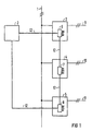
- FIG 1 shows an inventive converter system with three Inverters 3, 4 and 5, at the output 9, 10 and 11 one AC voltage is present.
- the inverters 3, 4 and 5 are in the exemplary embodiment in FIG 1 inverter. she can also be converters. In this case it is due the outputs 9, 10 and 11 of the inverters 3, 4 and 5 DC voltage on.
- the inverters 3, 4 and 5 are over a Power supply network 1 supplied with electrical energy. To generate DC voltage or current or to generate of alternating voltage or current with a suitable frequency the inverters 3, 4 and 5 can be switched on and / or off Power semiconductors.
- the control and coordination of the Power semiconductors of inverters 3, 4 and 5 are made using an automation device 2, the fiber optic 12 with intelligent interfaces 6, 7 and 8 of the converter 3, 4 and 5 is connected. Via the intelligent interfaces 6, 7 and 8 are the control commands of the automation device 2 to the power semiconductors of the corresponding Inverters 3, 4 and 5 forwarded.
- the intelligent interfaces 6, 7 and 8 are synchronized. If there is only one converter or converter are allowed to switch independently of one another, then synchronization takes place of the power units does not matter.
- the invention Solution then essentially refers to the Use of a fast serial bus system instead of many Individual connections for coupling control and regulation with Power section, whereby a converter mostly dimensions in the Order of magnitude e.g. 2m x 1m x 2m.
- the baud rate of the serial signal was chosen to be 40 Mbaud. This corresponds to a data rate of 2 16-bit words per microseconds.
- All data to be transmitted are organized in telegrams.
- the telegrams begin and end with a command byte, recognized as such by the TAXIChips.
- Each station can transmit at any time. There is no chosen one Master or master transfer.
- this telegram becomes in each station with its priority in the first data byte registered after the start command byte of the telegram.
- the telegram is received and the byte is delayed again by 2 bytes following station in the ring (echo). It is independent from the question of whether the telegram addresses the respective station.
- the priority of the telegram to be sent is higher than a telegram recognized in reception or echo, then that Echo telegram ignored and immediately the telegram to be sent began.
- the sending station of the lower prioritized telegram based on the circulated echo recognize that another telegram begins before your own received at the end. Because of this, this station becomes the Send request after receiving or echo of the Prioritize telegram repeat from the beginning.
- the same mechanism also applies if 2 stations at the same time start sending and this due to the turnaround time cannot find each other in the ring. At the same The station number decides the priority of the telegrams Priority.
- the control and regulation determined on the basis of software algorithms (e.g. field-oriented control with the following Tax rate) the times or duration for individual positions of the power valves.
- the positions of the power valves can be transmitted coded, e.g. with the 3-point converter with 2 bits for 3 sensible combinations of Control of 4 valves.
- control and regulation then Power section several consecutive in one sampling time the software calculates valve switching commands with valve position and time or period of time transmitted.
- Control information and related information Sampling information for analog value acquisition.
- the switching information is processed in the power section, in that when receiving telegrams via software in a FIFO (First In First Out Buffer) time differences or times and switching information one after the other be read out after the respective time has elapsed. On Time counter (hardware) realizes the right one Switching point accurate to less than 1 us. If the information is read from the FIFO for triggering analog values an integrator latched by hardware. It will be in the power section a telegram generates that on the control and regulation triggers the sampling time interrupt. In another due to time constraints analogue values generated after that, analog values are sent, in the sampling time interrupt of the control and regulation be used.
- FIFO First In First Out Buffer
- the time regime is thus processed by the switching information determined in the power section.
- the power section is for receiving telegrams and generating telegrams an extensive hardware circuit available, in a freely programmable logic circuit (LCA, type Xilinx) is realized.
- the generation of the switching information is also realized via another LCA, as is the Acquisition and digital integration of the analog values.
- LCAs makes technical sense and is due to this adaptation to different projects (number of valves etc.) may be mandatory, but not mandatory due to the solution according to the invention.
- CPU Central Processing Unit, microprocessor
- SAB C 165 16-bit controller with onchip functions.
- the CPU is completed with external RAM 256 kByte and external Flash-Eprom.
- the time is synchronized in several power units absolutely necessary if these spatially separated power units (Power cabinets) on the same consumer (Motor) or switch from the same network.
- the time is synchronized in several power units desirable, even if different consumers or network phases be switched because it has problems with floating Sampling times are bypassed.
- the synchronization of the times in power units is off View of the switching of the power valves with at least one Accuracy of less than 10 ⁇ s necessary, inaccuracies of this
- the order of magnitude can be compensated with compensating chokes. Because of the desire to minimize these balancing chokes or sensitive residual current control, if necessary with higher valve switching frequencies, e.g. with IGBT transistors possible, the time differences should be significantly better can be realized as 1 ⁇ s.
- the solution according to the invention allowed without using technology at the worst case limit an accuracy of neighboring stations with +/- 50 ns and accuracy of more distant stations in the ring +/- number of stations times 50 ns.
- the system clock of 20 used MHz is standard for the CPU system and good from the LCAs to process.
- a station in the ring is the master timer and contains one Time counter that is at least over 2 maximum sampling times maps the time.
- the counter can revolve.
- the resolution of the time count is e.g. 250 ns.
- the Counter with a cycle time of 16 ms has a bit number of 16 bits.
- All stations are synchronized from the master timer.
- the time pulse formation takes place e.g. 128 ⁇ s. It is derived from the 0-passage of the corresponding lower counter part of the master timer, in this case from the bottom 9 bit. More specifically, the time pulse becomes 1020 times 50 ns before the zero crossing generated, i.e. in the example at the counter reading 204 Zero crossing.
- the master timer works with the same clock as that Telegram control.
- a system clock of 50 ns is used where every 5th clock edge has a switching effect. This is with a central enable signal the synchronous flip-flop realized.
- This release signal is called CLKL for short (Clock for telegram traffic Lx), the central clock of 20 MHz is called CLKC ("C" because it is also used by the CPU).
- the otherwise running telegram traffic processes this time information without interference.
- For an active telegram generator the generation of data is suspended for this time, so the time pulse is passed on as an echo.
- the time pulse acts like an information break.
- the time pulse is recognized based on its command byte.
- the receiving station has a non-synchronous with the sending station Beat position and a beat in tolerance up to +/- 1 per mille.
- the strobe signal after the serial-parallel conversion in the TAXIChip of the receiver but with the clock position of the transmitter, since clock position of the serial signal.
- clock position means here in particular the location of the strobe or data change after the serial-parallel conversion (determined by Clock of the transmitter) to the central release clock CLKL.
- CLKL works synchronously with telegram processing and that Forwarding the telegram to the next station in the ring.
- the CLKL has a period of 250 ns.
- the central clock for the Processing CLKC works with 50 ns.
- This synchronization circuit takes one into account Difference of the clock frequencies between the transmitting station and the own cycle of max. +/- 1 per mille, that is expresses that information has to be delayed more and more, if the send clock e.g. is higher. Up to the end of a telegram no data loss may occur.
- This synchronization circuit provides pulses with which a counter can be zeroed and started, the clock position of strobe on the serial-parallel converter of the time pulse command byte determined to CLKL, including one at ongoing telegram traffic necessary additional Delay by 1 CLKL period.
- This counter works with the System clock CLKC (50 ns) and thus determines a delay in the range 0 to 9 in units of 50 ns. Due to the Clocking with the system clock 50 ns results in a Uncertainty of 50 ns.
- This value of the delay due to the synchronization of the received signal on the CLKL is now of the received Subtracted time information.
- the time information is converted from the byte after the time command byte (bits 9 to 2) and taken from the command byte (bit 1 and 0).
- This time information becomes the CLKL-synchronous point in time a 10 bit wide counter is loaded and started, which with the System clock CLKC counts. When the zero crossing is reached this counter is stopped. The zero crossing takes place as part of the 50 ns CLKC clock synchronized with the Zero crossing of the master timer. This is the impulse of the Timers in this station.
- the time information is passed on as an echo, namely with the corrected time information as just described.
- the subsequent station again corrects this time information with two components in mind: synchronization the location of the information received for processing and Runtime of the signal.
- An error of 50 ns due to the undetectable location of the CLKC clocks of the stations accumulate and determine the accuracy.
- this is exactly 50 ns (CLKC) Time at which the timer in the lower e.g. 9 bit at 250 ns resolution should have zero crossing.
- the counter can be a level deviate from 0, and slightly deviate if Time information was continuously received.
- the predecessor for the timer of normal value 5 (CLKC of 50 ns to Resolution changed to 250 ns) to the value 4 or 6, depending on whether a positive or negative deviation was detected.
- the deviation is in the register for this cycle counted down (this is a counter register).
- a time step will then take 200 or 300 ns followed from normal 250 ns.
- the central release clock becomes the prescaler for the meter CLKE for all time synchronous circuits (not for the Telegram traffic!) Derived. This CLKE runs in all of them Stations synchronously as part of the above Accuracy.
- the counter is set once to the total time initialization via software via a normal telegram. The counter is then started at the first time pulse. each Deviation beyond the clock frequency tolerance is recognized as a serious system failure.
- the converter system according to the invention is preferably supplied electrical drives and for network compensation in Question. It is also preferably suitable for applications where power in the megawatt range is regulated and provided Need to become.
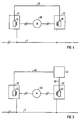
- FIG. 2 shows an inventive converter system with two Inverters for controlling or regulating a motor 17, wherein the outputs of the inverters 13 and 14 via inductors 18 and 19 are separated.
- the energy supply takes place via a Power supply network 1.
- the control of power semiconductors the converter 13 and 14 is carried out by means of an automation device 2, optical fibers 12 and intelligent Interfaces 15 and 16 in an analogous manner to the control of the converter system from FIG. 1.
- FIG 3 shows a converter system with two converters 20 and 21, wherein the control of the voltage or the current to the Outputs 22 and 23 of the converter 20 and 21 by means of a Automation device 24 takes place.
- the automation device 24 is integrated in the converter 20 and directly controls the Power semiconductor of the converter 20.
- the converter 21 has an intelligent interface 25 on that with the automation device 24 connected via an optical fiber 12 is.
- the control commands generated in the automation device 24 for the power semiconductors of the converter 21 via the optical fiber 12 to the intelligent interface 25 transferred to the power semiconductor of the converter 21 according to the control commands from the automation device 24 controls.
- the power supply of the converter 20 and 21 takes place via an energy supply network 1.
- FIG. 4 shows an inventive converter system for control of a motor 30 in tandem by means of two converters 31 and 32, which have a power supply network 1 Energy are supplied.
- the converter 31 is controlled via an automation device 34, via which likewise the converter 32 is controlled with the automation device 34 via an optical fiber 33 and an intelligent Interface 35 is connected.
- the control commands of the automation device 34 are of the intelligent Interface 35 to the power semiconductors of the converter 32 passed.
- FIG. 5 also shows a motor 30 with two converters 31 and 32 in a tandem circuit.
- the energy supply takes place thereby via an energy supply network 1.
- the power semiconductors the converter 31 and 32 are via an automation device 41 controlled, that via optical fibers 40 is connected to intelligent interfaces 42 and 43.
- the intelligent ones integrated in the inverters 31 and 32 Interfaces 42 and 43 give the control commands of the automation device 41 to the power semiconductors of the inverters 31 and 32 further.
Landscapes
- Engineering & Computer Science (AREA)
- Power Engineering (AREA)
- Remote Monitoring And Control Of Power-Distribution Networks (AREA)
- Inverter Devices (AREA)
- Information Transfer Systems (AREA)
Description
- wobei der Stromfluß durch die Leistungshalbleiter durch Einstellung der Ein- bzw. Ausschaltzeitpunkte für die Leistungshalbleiter beeinflußbar ist,
- wobei die gewünschte Gesamtspannung bzw. der gewünschte Gesamtstrom am Ausgang der Umrichter durch geeignete Steuerung der Ein- bzw. der Ausschaltzeitpunkte der einzelnen Leistungshalbleiter der Umrichterr beeinflußbar ist,
- wobei diesen Umrichtern zumindest ein von ihm räumlich getrenntes Automatisierungsgerät, das logisch mit den Leistungshalbleitern über zumindest ein Bussystem verbunden ist, zugeordnet ist, worüber die gewünschten Ein- bzw. Ausschaltzeitpunkte der einzelnen Leistungshalbleiter einstellbar sind,
- wobei jedem Umrichter eine frei programmierbare Busschnittstelle zugeordnet ist, die die gewünschten Ein- bzw. Ausschaltzeitpunkte für die Leistungshalbleiter des Umrichters empfängt und die Leistungshalbleiter zum gewünschten Zeitpunkt ein- bzw. ausschaltend ausgebildet ist,
- und wobei das Automatisierungsgerät oder ein Umrichter ein Zeitnormal sendend ausgebildet ist, das die einzelnen frei programmierbaren Schnittstellen mit einer Präzision von 10µs oder genauer zeitlich synchronisiert.
- FIG 1
- ein erfindungsgemäßes Umrichtersystem,
- FIG 2
- ein erfindungsgemäßes Umrichtersystem zur Steuerung eines Motors mit räumlich getrennten parallel geschalteten Leistungsteilen,
- FIG 3
- ein erfindungsgemäßes Umrichtersystem mit einem integrierten Automatisierungsgerät und zwei räumlich getrennten Leistungsteilen,
- FIG 4
- ein erfindungsgemäßes Umrichtersystem zur Steuerung eines Motors in Tandemschaltung,
- FIG 5
- ein erfindungsgemäßes Umrichtersystem zur Steuerung eines Motors in Tandemschaltung in alternativer Ausgestaltung.
- Codierung eines parallelen Bytes (8 bit) erfolgt in 10 seriellen Bit-Informationen in zwei sogenannten 4B-5B-Codierungen.
- Die serielle Information ist damit so beschaffen, daß nie mehr als 3 gleiche Bitinformationen hintereinander stehen. Nach spätestens 3 seriellen Bit kommt ein Signalwechsel auf der seriellen Seite. Damit ist über eine PLL-Schaltung (Phase Look Loop) die Taktrückgewinnung des Schiebetaktes aus der seriellen Information möglich.
- Ein bestimmter Signalverlauf, der aufgrund der 4B-5B-Codierung
als Datencode nie vorkommt, wird als Sync-Zeichen
erkannt. Damit wird die Byte-Synchronisation der
seriellen-parallel-Wandlung erreicht.
Bei jedem Byte der seriell-parallel-Wandlung, auch bei SYNC-Zeichen-Empfang, wird am IC eines von zwei Strobe-Signalen erzeugt, entweder Command-Strobe oder Daten-Strobe bei erkannten Daten-Codierungen. - Bestimmte Codierungen des seriellen Signales, die keine
Datencodierungen sind, werden als Command-Codierungen
erkannt. Bei der verwendeten 8-bit Datenbreite mit der 4B-5B-Codierung
gibt es 10 nutzbare Commdand-Codierungen.
Diese werden bei der erfindungsgemäßen Lösung als Daten-Rahmen verwendet (Beginn und Ende-Kennzeichnung der Datentelegramme). - Das Auftreten bestimmter Codierungen im seriellen Signal, die weder dem SYNC-Zeichen noch den Command-Codierungen und Datencodierungen zuzuordnen sind, werden als Datenübetragungsstörung (Violation) erkannt und an einem Pin des IC mit Strobe synchron angezeigt.
- Es gibt auch die Möglichkeit, 9 oder 10 bits pro Datenwort zu übertragen, mit einer entsprechenden 5B/6B-Codierung. Diese wird bei der erfindungsgemäßen Lösung nicht verwendet.
- 1 Byte Absendercode (4 bit) und Priorität (max. 4 bit, genutzt 3 bit)
- 2 Byte Ziel-Adresse der Information, jedes bit aus 16 ist einer Station zugeordnet, es können somit eine, mehrere oder alle Stationen adressiert werden.
- 1 Byte BufferNr der Information in 6 bit und 1 bit Information,
ob beim Empfang Interrupt ausgelöst werden
soll.
Aufgrund der BufferNr werden die Daten in den richtigen RAM-Bereich in der Empfängerstation (Teil des CPU-Rams, Zugriff über DMA (Direct Memory Access) geschrieben. Damit ist kein Softwareaufwand für die Rangierung von Daten in die richrigen Arbeitsbereiche notwendig. - 1 Byte Wiederholung der BufferNr mit XOR-Maske und verschobenen Bits, als Informationssicherung. Das Telegramm ist nur gültig, wenn dieses Byte zum vorangegangenen paßt. Die Überprüfung erfolgt durch Hardware.
- 2 Byte Länge des Telegrammes in Worte ä 16 bit. Nach Verarbeitung der Informationen kann hier 0 eingetragen werden. Wenn neue Daten übertragen werden, dann soll hier nicht 0 stehen. Damit kann erkannt werden: Neue Daten vorhanden. Das ist eine Semaphorenfunktion für die Verarbeitung der Daten.
- 2 Byte Kenn-Nummer des Telegrammes. Aufeinanderfolgende Telegramme sollten nie die gleiche Kennummer tragen, einfachkeitshalber sollte diese immer inkrementiert werden. Damit ist zum einen erkennbar, ob kein Telegramm fehlt, zum anderen ist erkennbar, daß ein neues Telegramm empfangen wurde.
- Wird bei einer Störung z.B. nur die Länge übertragen, dann kann aufgrund der unveränderten Kennummer erkannt werden, daß keine neuen Daten übertragen wurden.
- Auf dem Platz Datenbeginn + Telegrammlänge wird die Kennummer wie vorn nochmals wiederholt. Das ist der entscheidende Mechanismus zur Erkennung der Datenkonsistenz. Ist die Kennummer vorn und hinten nicht identisch, dann ist das Telegramm entweder eben noch in Übertragung begriffen oder es ist aufgrund eines Fehlers abgebrochen worden.
- Eines von 4 Kennungs-Command-Byte für den Zeitimpuls
- Ein Datenbyte mit dem Inhalt 255 (alle bit gesetzt).
- konstante Verzögerung des seriellen Eingangssignales zum seriellen Ausgangssignal im Ring aufgrund der inneren Verarbeitung,
- Laufzeit des seriellen Signales vom Sender zum Empfänger aufgrund physikalischer Verzögerungszeiten, insbesondere Laufzeit im LWL.
Claims (12)
- Umrichtersystem mit mehreren Umrichtern (3,4,5;13,14;20, 21;31,32), insbesondere zur Versorgung von elektrischen Antrieben (17,30) mit Wechselstrom bzw. -spannung mit spezifisch angepaßter Frequenz oder zur dynamischen Netzkompensation, wobei diese Umrichter (3,4,5;13,14;20,21;31,32) abschaltbare Leistungshalbleiter aufweisen,wobei der Stromfluß durch die Leistungshalbleiter durch Einstellung der Ein- bzw. Ausschaltzeitpunkte für die Leistungshalbleiter beeinflußbar ist,wobei die gewünschte Gesamtspannung bzw. der gewünschte Gesamtstrom am Ausgang der Umrichter (3,4,5;13,14;20,21;31, 32) durch geeignete Steuerung der Ein- bzw. der Ausschaltzeitpunkte der einzelnen Leistungshalbleiter der Umrichter (3,4,5;13,14;20,21;31,32) beeinflußbar ist,wobei diesen Umrichtern (3,4,5;13,14;31,32) zumindest ein von ihm räumlich getrenntes Automatisierungsgerät (2,41), das logisch mit den Leistungshalbleitern über zumindest ein Bussystem verbunden ist, zugeordnet ist, worüber die gewünschten Ein- bzw. Ausschaltzeitpunkte der einzelnen Leistungshalbleiter einstellbar sind,wobei jedem Umrichter (3,4,5;13,14;20,21;31,32) eine frei programmierbare Busschnittstelle (6,7,8;15,16;25,35;42,43) zugeordnet ist, die die gewünschten Ein- bzw. Ausschaltzeitpunkte für die Leistungshalbleiter des Umrichters (3,4,5;13,14;21;31,32) empfängt und die Leistungshalbleiter zum gewünschten Zeitpunkt ein- bzw. ausschaltend ausgebildet ist,und wobei das Automatisierungsgerät (2,41) oder ein Umrichter (3,4,5;13,14;20,21;31,32) des Umrichtersystems ein Zeitnormal sendend ausgebildet ist, das die einzelnen frei programmierbaren Schnittstellen (6,7,8;15,16;25,35;42,43) mit einer Präzision von 10µs oder genauer zeitlich synchronisiert.
- Umrichtersystem nach Anspruch 1,
dadurch gekennzeichnet, daß das Bussystem als serielles Bussystem ausgebildet ist. ist. - Umrichtersystem nach Anspruch 2,
dadurch gekennzeichnet, daß das Bussystem als Lichtwellenleiter (12,33,40) ausgebildet ist. - Umrichtersystem nach Anspruch 2 oder 3,
dadurch gekennzeichnet, daß das Bussystem als Ring, der zumindest ein Automatisierungsgerät (2) und zumindest zwei Umrichter (3,4,5;13,14) verbindet, ausgebildet ist. - Umrichtersystem nach Anspruch 1,
dadurch gekennzeichnet, daß das Zeitnormal die einzelnen frei programmierbaren Schnittstellen (6,7,8;15,16;25,35;42,43) mit einer Präzision von 50 ns oder genauer zeitlich synchronisiert. - Umrichtersystem nach einem oder mehreren der Ansprüche 1 bis 5, dadurch gekennzeichnet, daß das Umrichtersystem ein einziges Automatisierungssystem (2,24,34,41) aufweist.
- Umrichtersystem nach Anspruch 6,
dadurch gekennzeichnet, daß das Automatisierungsgerät (24,34) räumlich einem Umrichter (20,31) zugeordnet ist. - Umrichtersystem nach einem oder mehreren der Ansprüche 1 bis 7, dadurch gekennzeichnet, daß die frei programmierbaren Schnittstellen (6,7,8;15,16;25, 35;42,43) Meßwerte bezüglich Strom und Spannung über das Bussystem an das Automatisierungsgerät (2,41) übertragend ausgebildet ist.
- Umrichtersystem nach einem oder mehreren der Ansprüche 1 bis 8,
dadurch gekennzeichnet, daß das Bussystem die Informationen, wie z.B. Ein- und/oder Ausschaltzeitpunkt, Meßwerte oder das Zeitnormal, über das Bussystem mit einer Rate von mindestens 5 MBaud, vorzugsweise mit einer Rate von mindestens 20 Mbaud übertragend ausgebildet ist. - Umrichtersystem nach Anspruch 1,
dadurch gekennzeichnet, daß das Bussystem die Informationen, wie z.B. Ein- und/oder Ausschaltzeitpunkt, Meßwerte oder das Zeitnormal, mit einer Rate von 40 Mbaud übertragend ausgebildet ist. - Umrichtersystem nach einem oder mehreren der Ansprüche 1 bis 10,
dadurch gekennzeichnet, daß die Umrichter (3,4,5;13,14;20,21;31,32) jeweils in bezug auf Dauerlast in einem Leistungsbereich von 1 bis 20 Megawatt, vorteilhafterweise von 2 bis 10 Megawatt, arbeitend ausgebildet sind. - Umrichtersystem nach einem oder mehreren der Ansprüche 1 bis 11,
dadurch gekennzeichnet, daß die Umrichter (3,4,5;13,14;20,21;31,32) jeweils in bezug auf Stoßlast in einem Leistungsbereich von 2 bis 30 Megawatt, vorteilhafterweise von 4 bis 20 Megawatt, arbeitend ausgebildet sind.
Applications Claiming Priority (3)
| Application Number | Priority Date | Filing Date | Title |
|---|---|---|---|
| DE19620442 | 1996-05-21 | ||
| DE19620442A DE19620442A1 (de) | 1996-05-21 | 1996-05-21 | Unrichtersystem |
| PCT/DE1997/000943 WO1997044887A1 (de) | 1996-05-21 | 1997-05-09 | Umrichtersystem |
Publications (2)
| Publication Number | Publication Date |
|---|---|
| EP0900472A1 EP0900472A1 (de) | 1999-03-10 |
| EP0900472B1 true EP0900472B1 (de) | 2002-07-24 |
Family
ID=7794906
Family Applications (1)
| Application Number | Title | Priority Date | Filing Date |
|---|---|---|---|
| EP97922901A Expired - Lifetime EP0900472B1 (de) | 1996-05-21 | 1997-05-09 | Umrichtersystem |
Country Status (5)
| Country | Link |
|---|---|
| US (1) | US6021057A (de) |
| EP (1) | EP0900472B1 (de) |
| CN (1) | CN1225758A (de) |
| DE (2) | DE19620442A1 (de) |
| WO (1) | WO1997044887A1 (de) |
Families Citing this family (18)
| Publication number | Priority date | Publication date | Assignee | Title |
|---|---|---|---|---|
| AT6706U1 (de) * | 1999-10-11 | 2004-02-25 | Innova Patent Gmbh | Elektromotor |
| DE10205832A1 (de) * | 2002-02-13 | 2003-08-28 | Semikron Elektronik Gmbh | Ansteuerung für Stromrichterventile |
| FI117145B (fi) * | 2004-11-26 | 2006-06-30 | Vacon Oyj | Mittausmenetelmä ja -järjestely |
| US20060265105A1 (en) * | 2005-05-20 | 2006-11-23 | Hughes Albert R | Loop-powered field instrument |
| US7480487B2 (en) * | 2005-05-20 | 2009-01-20 | Dresser, Inc. | Power regulation for field instruments |
| DE102005045957A1 (de) * | 2005-09-26 | 2006-11-16 | Siemens Ag | Verfahren und Vorrichtung zur Übertragung von Signalen |
| US7688607B2 (en) | 2005-09-30 | 2010-03-30 | Volterra Semiconductor Corporation | Voltage regulator with inductor banks |
| US7522436B2 (en) | 2005-09-30 | 2009-04-21 | Volterra Semiconductor Corporation | Master-slave with adaptation control including slave current checking |
| US7514909B2 (en) * | 2005-09-30 | 2009-04-07 | Voiterra Semiconductor Corporation | Voltage regulator with communication ring scheme |
| US8188694B2 (en) * | 2010-07-16 | 2012-05-29 | Rockwell Automation Technologies, Inc. | Parallel power inverter motor drive system |
| US8575882B2 (en) * | 2010-07-16 | 2013-11-05 | Rockwell Automation Technologies, Inc. | Power layer generation of inverter gate drive signals |
| CN101964544B (zh) * | 2010-09-20 | 2014-03-12 | 中国电力科学研究院 | 一种hvdc换流阀晶闸管级运行状况监视方法 |
| AT513542B1 (de) * | 2012-11-15 | 2014-07-15 | Fronius Int Gmbh | Verfahren und Anordnung zur Datenkommunikation zwischen einem Wechselrichter und einer Netzüberwachungseinheit |
| US9793803B2 (en) * | 2013-03-15 | 2017-10-17 | Infineon Technologies Austria Ag | Power converter circuit |
| EP2797217A1 (de) * | 2013-04-23 | 2014-10-29 | ABB Technology AG | Verteilte Steuerungen für einen Leistungselektronikwandler |
| CN103401448A (zh) * | 2013-08-15 | 2013-11-20 | 上海宝准电源科技有限公司 | 一种数据复合通讯在逆变器中使用方法 |
| DK2887547T3 (en) | 2013-12-20 | 2018-07-23 | Abb Oy | Offsetting power from power semiconductors |
| CN106849021A (zh) * | 2017-03-17 | 2017-06-13 | 深圳市禾望电气股份有限公司 | 半导体开关过流检测方法及变流器 |
Family Cites Families (7)
| Publication number | Priority date | Publication date | Assignee | Title |
|---|---|---|---|---|
| US5187656A (en) * | 1984-12-25 | 1993-02-16 | Fanuc Ltd. | Servomotor drive control system |
| US4994950A (en) * | 1990-07-31 | 1991-02-19 | Eaton Corporation | Waveform generator for inverter control |
| US5045988A (en) * | 1990-07-31 | 1991-09-03 | Eaton Corporation | Isolated adjustable frequency AC inverter control |
| US5499177A (en) * | 1992-04-22 | 1996-03-12 | Fuji Electric Co., Ltd. | Inverter device with a circuit for generating pulse width modulation signals |
| JPH08289591A (ja) * | 1995-04-14 | 1996-11-01 | Toray Eng Co Ltd | 駆動制御ユニット |
| DE69738593T2 (de) * | 1996-06-24 | 2009-04-23 | Sanyo Electric Co., Ltd., Moriguchi | Stromversorgungssystem mit Systemverbindung |
| US5847950A (en) * | 1997-02-19 | 1998-12-08 | Electronic Measurements, Inc. | Control system for a power supply |
-
1996
- 1996-05-21 DE DE19620442A patent/DE19620442A1/de not_active Withdrawn
-
1997
- 1997-05-09 WO PCT/DE1997/000943 patent/WO1997044887A1/de not_active Ceased
- 1997-05-09 CN CN97196623A patent/CN1225758A/zh active Pending
- 1997-05-09 EP EP97922901A patent/EP0900472B1/de not_active Expired - Lifetime
- 1997-05-09 DE DE59707793T patent/DE59707793D1/de not_active Expired - Lifetime
- 1997-05-09 US US09/194,449 patent/US6021057A/en not_active Expired - Fee Related
Also Published As
| Publication number | Publication date |
|---|---|
| WO1997044887A1 (de) | 1997-11-27 |
| CN1225758A (zh) | 1999-08-11 |
| DE59707793D1 (de) | 2002-08-29 |
| US6021057A (en) | 2000-02-01 |
| EP0900472A1 (de) | 1999-03-10 |
| DE19620442A1 (de) | 1997-11-27 |
Similar Documents
| Publication | Publication Date | Title |
|---|---|---|
| EP0816963B1 (de) | Verfahren zum Betrieb eines Antriebssystems und Vorrichtung zur Durchführung des Verfahrens | |
| WO1997044887A1 (de) | Umrichtersystem | |
| DE10041772C2 (de) | Taktgenerator, insbesondere für USB-Geräte | |
| DE69522267T2 (de) | Selbstsynchronisierte Schnittstelle | |
| EP1430627B1 (de) | Verfahren zur synchronisation von knoten eines kommunikationssystems | |
| EP0389662B1 (de) | Verfahren zum Synchronisieren der Phase von Taktsignalen zweier Taktgeneratoren in Kommunikationsnetzen | |
| EP1368728B1 (de) | Synchrones, getaktetes kommunikationssystem mit relativuhr und verfahren zum aufbau eines solchen systems | |
| EP1648116B1 (de) | Verfahren zur Übertragung von Daten in einem Kommunikationssystem | |
| EP1653651B1 (de) | Modulares numerisches steuergerät mit low-jitter synchronisation | |
| DE69220267T2 (de) | Pulsstopfanlage | |
| EP1648117B1 (de) | Verfahren zur Synchronisation in einem redundanten Kommunikationssystem | |
| EP0192120B2 (de) | Verfahren und Einrichtung zur Datenübertragung in der Fernwirktechnik | |
| DE3789791T2 (de) | Datenübertragungsvorrichtung. | |
| DE10047924A1 (de) | Gebersystem zur Lage-/Positionserfassung und/oder Geschwindigkeitserfassung und/oder Beschleunigungserfassung, darauf aufbauende Antriebsregelung sowie Verfahren zur Vernetzung einer Regelungseinheit mit einem oder mehreren Gebersystemen | |
| DE60104336T2 (de) | Fehlertolerante synchronisationseinrichtung für ein echtzeit-computernetzwerk | |
| EP4014422B1 (de) | Verfahren und vorrichtung zum synchronisieren von dezentralen steuervorrichtungen | |
| EP1886448B1 (de) | Universelles mess- oder schutzgerät | |
| EP1219071B1 (de) | Betriebsverfahren für einen datenbus für mehrere teilnehmer mit flexiblem zeitgesteuertem zugriff | |
| EP1179920A2 (de) | Datenbus für mehrere Teilnehmer | |
| EP1915661B1 (de) | Vorrichtung zur optimierung des leistungsverbrauchs einer elektrischen schaltungskomponente | |
| DE68910265T2 (de) | Verfahren zur Übertragung von Nachrichten mittels einer bidirektionalen Strecke, und Gerät zu dessen Durchführung. | |
| EP1648104A2 (de) | Kommunikationssystem und Verfahren zur Synchronisation desselben | |
| DE10206904A1 (de) | Kommunikation in einem verteilten Steuerungssystem mit Unterdrücken der zyklischen Kommunikation nach Äquidistanzverletzung | |
| DE2746299C3 (de) | Steuerschaltung zur Zündung von Thyristoren und deren Rückmeldung | |
| DE2441550C3 (de) | Verfahren und Schaltungsanordnung zur zeitgerechten Übernahme von binär codierten Datenzeichen zwischen zwei isochron arbeitenden Übertragungsstrecken in einem taktgesteuerten Datennetz |
Legal Events
| Date | Code | Title | Description |
|---|---|---|---|
| PUAI | Public reference made under article 153(3) epc to a published international application that has entered the european phase |
Free format text: ORIGINAL CODE: 0009012 |
|
| AK | Designated contracting states |
Kind code of ref document: A1 Designated state(s): BE DE FI FR GB |
|
| 17P | Request for examination filed |
Effective date: 19981105 |
|
| 17Q | First examination report despatched |
Effective date: 20001012 |
|
| GRAG | Despatch of communication of intention to grant |
Free format text: ORIGINAL CODE: EPIDOS AGRA |
|
| GRAG | Despatch of communication of intention to grant |
Free format text: ORIGINAL CODE: EPIDOS AGRA |
|
| GRAH | Despatch of communication of intention to grant a patent |
Free format text: ORIGINAL CODE: EPIDOS IGRA |
|
| GRAH | Despatch of communication of intention to grant a patent |
Free format text: ORIGINAL CODE: EPIDOS IGRA |
|
| GRAA | (expected) grant |
Free format text: ORIGINAL CODE: 0009210 |
|
| AK | Designated contracting states |
Kind code of ref document: B1 Designated state(s): BE DE FI FR GB |
|
| REG | Reference to a national code |
Ref country code: GB Ref legal event code: FG4D Free format text: NOT ENGLISH |
|
| REF | Corresponds to: |
Ref document number: 59707793 Country of ref document: DE Date of ref document: 20020829 |
|
| GBT | Gb: translation of ep patent filed (gb section 77(6)(a)/1977) |
Effective date: 20020927 |
|
| ET | Fr: translation filed | ||
| PLBE | No opposition filed within time limit |
Free format text: ORIGINAL CODE: 0009261 |
|
| STAA | Information on the status of an ep patent application or granted ep patent |
Free format text: STATUS: NO OPPOSITION FILED WITHIN TIME LIMIT |
|
| 26N | No opposition filed |
Effective date: 20030425 |
|
| PGFP | Annual fee paid to national office [announced via postgrant information from national office to epo] |
Ref country code: FI Payment date: 20050407 Year of fee payment: 9 |
|
| PGFP | Annual fee paid to national office [announced via postgrant information from national office to epo] |
Ref country code: GB Payment date: 20050505 Year of fee payment: 9 |
|
| PGFP | Annual fee paid to national office [announced via postgrant information from national office to epo] |
Ref country code: BE Payment date: 20050517 Year of fee payment: 9 |
|
| PGFP | Annual fee paid to national office [announced via postgrant information from national office to epo] |
Ref country code: FR Payment date: 20050520 Year of fee payment: 9 |
|
| PG25 | Lapsed in a contracting state [announced via postgrant information from national office to epo] |
Ref country code: GB Free format text: LAPSE BECAUSE OF NON-PAYMENT OF DUE FEES Effective date: 20060509 Ref country code: FI Free format text: LAPSE BECAUSE OF NON-PAYMENT OF DUE FEES Effective date: 20060509 |
|
| PG25 | Lapsed in a contracting state [announced via postgrant information from national office to epo] |
Ref country code: BE Free format text: LAPSE BECAUSE OF NON-PAYMENT OF DUE FEES Effective date: 20060531 |
|
| GBPC | Gb: european patent ceased through non-payment of renewal fee |
Effective date: 20060509 |
|
| REG | Reference to a national code |
Ref country code: FR Ref legal event code: ST Effective date: 20070131 |
|
| BERE | Be: lapsed |
Owner name: *SIEMENS A.G. Effective date: 20060531 |
|
| PG25 | Lapsed in a contracting state [announced via postgrant information from national office to epo] |
Ref country code: FR Free format text: LAPSE BECAUSE OF NON-PAYMENT OF DUE FEES Effective date: 20060531 |
|
| PGFP | Annual fee paid to national office [announced via postgrant information from national office to epo] |
Ref country code: DE Payment date: 20110718 Year of fee payment: 15 |
|
| REG | Reference to a national code |
Ref country code: DE Ref legal event code: R119 Ref document number: 59707793 Country of ref document: DE Effective date: 20121201 |
|
| PG25 | Lapsed in a contracting state [announced via postgrant information from national office to epo] |
Ref country code: DE Free format text: LAPSE BECAUSE OF NON-PAYMENT OF DUE FEES Effective date: 20121201 |