EP0899644A2 - Polarisationsspannungsstabilisierungsschaltung - Google Patents
Polarisationsspannungsstabilisierungsschaltung Download PDFInfo
- Publication number
- EP0899644A2 EP0899644A2 EP98306464A EP98306464A EP0899644A2 EP 0899644 A2 EP0899644 A2 EP 0899644A2 EP 98306464 A EP98306464 A EP 98306464A EP 98306464 A EP98306464 A EP 98306464A EP 0899644 A2 EP0899644 A2 EP 0899644A2
- Authority
- EP
- European Patent Office
- Prior art keywords
- voltage
- diode
- circuit
- voltage drop
- drop circuit
- Prior art date
- Legal status (The legal status is an assumption and is not a legal conclusion. Google has not performed a legal analysis and makes no representation as to the accuracy of the status listed.)
- Withdrawn
Links
- 230000000087 stabilizing effect Effects 0.000 title claims abstract description 22
- 239000003990 capacitor Substances 0.000 description 8
- 230000008859 change Effects 0.000 description 5
- 238000010586 diagram Methods 0.000 description 5
- 238000000034 method Methods 0.000 description 4
- 230000008569 process Effects 0.000 description 4
- 239000003381 stabilizer Substances 0.000 description 3
- JBRZTFJDHDCESZ-UHFFFAOYSA-N AsGa Chemical compound [As]#[Ga] JBRZTFJDHDCESZ-UHFFFAOYSA-N 0.000 description 2
- 230000005540 biological transmission Effects 0.000 description 2
- 238000006243 chemical reaction Methods 0.000 description 2
- 238000009499 grossing Methods 0.000 description 2
- 238000012986 modification Methods 0.000 description 2
- 230000004048 modification Effects 0.000 description 2
- 230000005236 sound signal Effects 0.000 description 2
- 238000004891 communication Methods 0.000 description 1
- 230000009467 reduction Effects 0.000 description 1
Images

Classifications
-
- G—PHYSICS
- G05—CONTROLLING; REGULATING
- G05F—SYSTEMS FOR REGULATING ELECTRIC OR MAGNETIC VARIABLES
- G05F3/00—Non-retroactive systems for regulating electric variables by using an uncontrolled element, or an uncontrolled combination of elements, such element or such combination having self-regulating properties
- G05F3/02—Regulating voltage or current
- G05F3/08—Regulating voltage or current wherein the variable is DC
- G05F3/10—Regulating voltage or current wherein the variable is DC using uncontrolled devices with non-linear characteristics
- G05F3/16—Regulating voltage or current wherein the variable is DC using uncontrolled devices with non-linear characteristics being semiconductor devices
- G05F3/20—Regulating voltage or current wherein the variable is DC using uncontrolled devices with non-linear characteristics being semiconductor devices using diode- transistor combinations
- G05F3/205—Substrate bias-voltage generators
Definitions
- the present invention relates to a bias voltage stabilizing circuit suitable for use in a bias voltage generating circuit for supplying a bias voltage to an amplifier circuit, notably a power amplifier circuit.
- a conventional bias voltage generating circuit will be described by an example in which it is used in a communication device such as a so-called codeless telephone or the like.
- a transmit signal lying within a 1.8GHz band which has been subjected to processes such as modulation, frequency conversion, etc. by a pre-stage processing circuit 31, is amplified to a predetermined power (of about 500Mw) by a power amplifier circuit 32, followed by transmission to an antenna 35 through an antenna switch circuit 33 and a band-pass filer 34.
- the signal received by the antenna 35 is inputted via the band-pass filter 34 and the antenna switch circuit 33 to a receiving circuit 36 where a predetermined process is effected on the signal to thereby obtain a voice or audio signal.
- the power amplifier circuit 32 comprises driver amplifiers 32a and 32b corresponding to two stages and a final amplifier 32c corresponding to one stage, for example.
- Unillustrated gallium arsenide (GaAs) transistors (hereinafter called “transistors”) are used in the respective stages. The gates of these transistors are respectively supplied with bias voltages from a bias voltage generating circuit 37.
- the bias voltage generating circuit 37 has a voltage multiplying rectifier 38, a smoothing circuit 39, and a bias voltage stabilizer or stabilizing circuit 40.
- the bias voltage generating circuit 37 performs voltage multiplication and rectification on a clock signal of about 10MHz generated from a clock signal generator circuit 41 by using a capacitor 38a and rectifier diodes 38b and 38c and smoothes the resultant signal by use of a resistor 39a and a capacitor 39b, thereby obtaining a negative bias voltage.
- the resultant bias voltage is stabilized by a zener diode (whose zener voltage is about 2 volts) 40a parallel-connected to the capacitor 39b and supplied to the gate of the unillustrated transistor of the final amplifier 32c. Further, the bias voltage is reduced to about minus 1.3 volts by a diode 40b, which is also supplied to the gates of the unillustrated transistors of the driver amplifiers 32a and 32b.
- the reason why the diode 40b is used to obtain the bias voltage (-1.3 volts) to be supplied to the driver amplifiers 32a and 32b is intended for a reduction in a change in bias voltage due to a change in bias current flowing through the driver amplifiers 32a and 32b.
- the zener voltage (2 volts) of the zener diode 40a which stabilizes the bias voltage, and a drop (about 0.7 volt) in the forward voltage of the diode 40b are kept constant.
- the zener voltage and the forward voltage also change as the ambient temperature changes.
- the zener voltage of the zener diode 40a is reduced and the forward voltage of the diode 40b is also lowered.
- the bias voltage changes with the rise and fall in temperature and the output power of the power amplifier circuit also changes.
- a problem arises in that transmitting power is not kept constant, thus resulting in interference with a call.
- a bias voltage stabilizing circuit comprising:
- a zener diode is parallel-connected to the dc voltage source and the resistors are connected to the second voltage drop circuit in series with the second diode.
- a zener diode is parallel-connected to the dc voltage source, a first resistor is connected to the first voltage drop circuit in series with the first diode, a second resistor is connected to the second voltage drop circuit in series with the second diode, and the resistance value of the second resistor is set larger than that of the first resistor.
- a bias voltage stabilizing circuit according to the present invention will hereinafter be described with reference to Figs. 1 through 3.
- a transmit signal lying within a 1.8GHz band which has been subjected to processes such as modulation, frequency conversion, etc. by a pre-stage processing circuit 1, is amplified to a predetermined power (of about 500mW) by a power amplifier circuit 2, followed by transmission to an antenna 5 through an antenna switch circuit 3 and a band-pass filer 4.
- a predetermined power of about 500mW
- the signal received by the antenna 5 is inputted via the band-pass filter 4 and the antenna switch circuit 3 to a receiving circuit 6 where a predetermined process is effected on the signal to thereby obtain a voice or audio signal.
- the power amplifier circuit 2 comprises driver amplifiers 2a and 2b corresponding to two stages and a final amplifier 2c corresponding to one stage, for example.
- Unillustrated gallium arsenide (GaAs) transistors (hereinafter called “transistors”) are respectively used in the respective stages.
- the gates of these transistors are respectively supplied with bias voltages from a bias voltage generating circuit 7.
- the bias voltage generating circuit 7 has a voltage multiplying rectifier 8, a smoothing circuit 9, and a bias voltage stabilizer or stabilizing circuit 10.
- the bias voltage generating circuit 7 performs voltage multiplication and rectification on a clock signal of about 10MHz generated from a clock signal generator or generating circuit 16 by using a capacitor 8a and rectifier diodes 8b and 8c and smoothes the resultant signal by use of a resistor 9a and a capacitor 9b, thereby obtaining a negative dc voltage used as a dc voltage source applied across the capacitor 9b.
- the resultant dc voltage is stabilized by the capacitor 9b, accordingly, a zener diode (whose zener voltage is about 2 volts) 10a parallel-connected to the dc voltage source, thus resulting in a first bias voltage, which in turn is supplied to the gate of the unillustrated transistor of the final amplifier 2c.
- a first voltage drop circuit 10b comprised of a first diode 11 and a first resistor 12 electrically series-connected to each other
- a second voltage drop circuit 10c comprised of a second diode 13 and a second resistor 14 electrically series-connected to each other are electrically connected in series with the zener diode 10a.
- the first voltage drop circuit 10b and the second voltage drop circuit 10c are electrically connected in parallel to the dc voltage source.
- a second bias voltage is obtained from a point (i.e., a point where the first resistor 12 of the first voltage drop circuit 10b and the second resistor 14 of the second voltage drop circuit 10c are electrically connected to each other in Fig.
- the first voltage drop circuit 10b and the second voltage drop circuit 10c are electrically connected to each other. Thereafter, the second bias voltage is supplied to the gates of the unillustrated transistors of the driver amplifiers 2a and 2b.
- the zener diode 10a, the first voltage drop circuit 10b and the second voltage drop circuit 10c constitute the bias voltage stabilizer circuit 10.
- the first diode 11, the first resistor 12, the second diode 13 and the second resistor 14 constitutes a closed loop together with the dc voltage source. A loop current flows in the closed loop.
- Fig. 2 shows the bias voltage stabilizing circuit 10 shown in Fig. 1 in the form of an equivalent circuit.
- a dc voltage source 15 shows a voltage V developed across the capacitor 9b shown in Fig. 1.
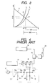
- Fig. 3 is a diagram showing operation characteristics of the first voltage drop circuit 10b and the second voltage drop circuit 10c.
- a curve T1 represents a characteristic curve at ordinary temperature, for example, of two diodes: the first diode 11 and the second diode 13.
- a curve T2 indicates a high-temperature characteristic curve at a temperature higher than the ordinary temperature.
- a curve R shows a load curve of two resistors: the first resistor 12 and the second resistor 14.
- the first diode 11 and the second diode 13 will be defined as having characteristics identical to each other.
- the zener diode 10a shown in Fig. 1 is omitted in Fig. 2.
- the respective voltage drops developed across the first resistor 12 and the second resistor 14 result in voltages obtained by making a fraction of VR1 according to the magnitudes of their resistance values.
- the voltage at the point A of connection between the first voltage drop circuit 10b and the second voltage drop circuit 10c results in one obtained by adding the voltage drop developed across the second resistor 14 to the voltage drop Vl/2 developed across the second diode 13.
- the resistance value of the first resistor 12 and the resistance value of the second resistance 14 are identical to each other, then the voltage at the connecting point A results in 1/2 the voltage V of the dc voltage source.
- This voltage drop VR2 becomes larger than the voltage drop VR1 developed across the two resistors 12 and 14 at the ordinary temperature. Namely, as the temperature increases, the voltage drop developed across the first resistor 12 and the second resistor 14 becomes relatively larger than the voltage drop developed across the first diode 11 and the second diode 13.
- the voltage at the connecting point A reaches the same V/2 at both ordinary and high temperatures.
- the resistance value of the second resistor 14 is set larger than that of the first resistor 12, then the voltage at the connecting point A becomes higher at the high temperature than at the ordinary temperature.
- the resistance value of the second resistor 14 is set smaller than that of the first resistor 12, then the voltage at the connecting point A becomes lower at the high temperature than at the ordinary temperature.
- the first voltage drop circuit 10b includes one first diode and the second voltage drop circuit 10c includes one second diode
- the number of diodes is not necessarily limited to one. They may include a plurality of diodes respectively.
- the voltage at the connecting point A can be set to a desired value by providing the plurality of diodes.
- the voltage at the connecting point A can be held constant without depending on the ambient temperature if the resistance value of the first resistor 12 in the first voltage drop circuit 10b is set larger than that of the second resistor 14 in the second voltage drop circuit 10c.
- the voltage at the connecting point A can be kept constant without depending on the ambient temperature if the resistance value of the first resistor 12 in the first voltage drop circuit 10b is set smaller than that of the second resistor 14 in the second voltage drop circuit 10c.
- the zener diode 10a When the zener diode 10a is electrically parallel-connected to the dc voltage source 15 as shown in Fig. 1, the zener voltage of the zener diode 10a becomes low with the rise in ambient temperature and hence the voltage of the dc voltage source 15 becomes low. Therefore, if the resistance value of the second resistor 14 is set greater than that of the first resistor 12, then the voltage at the connecting point A can be set equally at both the ordinary and high temperatures. Alternatively, the voltage at the connecting point A can be set equally at both the ordinary and high temperatures even when the second resistor 14 is provided only for the second voltage drop circuit 10c without the first voltage drop circuit 10b being provided with the first resistor 12.
- the transmitting power of a power amplifier circuit 2 employed in a telephone set can be kept substantially constant without depending on the ambient temperatures by using such a bias voltage stabilizing circuit, whereby a normal call can be made.
- the bias voltage stabilizing circuit of the present invention comprises a dc voltage source, a first voltage drop circuit having a first diode, and a second voltage drop circuit having a second diode.
- the first voltage drop circuit and the second voltage drop circuit are electrically series-connected to each other and electrically parallel-connected to the dc voltage source.
- resistors are electrically connected to at least one of the first voltage drop circuit and the second voltage drop circuit in series with either the first diode or the second diode.
- a closed loop is formed by the dc voltage source, the first diode, the second diode and the resistors, and the voltage at a point where the first voltage drop circuit and second voltage drop circuit are electrically connected to each other, is set as a bias voltage.
- the voltage at the point of connection between the first voltage drop circuit and the second voltage drop circuit can be kept substantially constant without depending on a change in ambient temperature. Further, if the voltage at the connecting point is used as a bias voltage for a power amplifier circuit, then output power thereof can be also held substantially constant.
- a zener diode is electrically parallel-connected to a dc voltage source, and a resistor is electrically connected to a second voltage drop circuit in series with a second diode. Therefore, the voltage of the dc voltage source can be stabilized and the voltage at a connecting point can be also held constant without depending on the temperature.
- a zener diode is electrically parallel-connected to a dc voltage source, and a first resistor is electrically connected to a first voltage drop circuit in series with a first diode. Further, a second resistor is electrically connected to a second voltage drop circuit in series with a second diode, and the resistance value of the second resistor is set larger than that of the first resistor. Therefore, the voltage of the dc voltage source can be stabilized in the same manner as described above and the voltage at a connecting point can be also kept constant without depending on the temperature.
Landscapes
- Engineering & Computer Science (AREA)
- Physics & Mathematics (AREA)
- Microelectronics & Electronic Packaging (AREA)
- Nonlinear Science (AREA)
- Electromagnetism (AREA)
- General Physics & Mathematics (AREA)
- Radar, Positioning & Navigation (AREA)
- Automation & Control Theory (AREA)
- Amplifiers (AREA)
- Control Of Electrical Variables (AREA)
- Direct Current Feeding And Distribution (AREA)
Applications Claiming Priority (2)
| Application Number | Priority Date | Filing Date | Title |
|---|---|---|---|
| JP9235652A JPH1174736A (ja) | 1997-09-01 | 1997-09-01 | バイアス電圧安定化回路 |
| JP235652/97 | 1997-09-01 |
Publications (2)
| Publication Number | Publication Date |
|---|---|
| EP0899644A2 true EP0899644A2 (de) | 1999-03-03 |
| EP0899644A3 EP0899644A3 (de) | 1999-05-06 |
Family
ID=16989196
Family Applications (1)
| Application Number | Title | Priority Date | Filing Date |
|---|---|---|---|
| EP98306464A Withdrawn EP0899644A3 (de) | 1997-09-01 | 1998-08-13 | Polarisationsspannungsstabilisierungsschaltung |
Country Status (2)
| Country | Link |
|---|---|
| EP (1) | EP0899644A3 (de) |
| JP (1) | JPH1174736A (de) |
Family Cites Families (2)
| Publication number | Priority date | Publication date | Assignee | Title |
|---|---|---|---|---|
| JPS60253090A (ja) * | 1984-05-30 | 1985-12-13 | Hitachi Ltd | 半導体装置 |
| JPH09162641A (ja) * | 1995-12-05 | 1997-06-20 | Alps Electric Co Ltd | 電圧制御発振器 |
-
1997
- 1997-09-01 JP JP9235652A patent/JPH1174736A/ja not_active Withdrawn
-
1998
- 1998-08-13 EP EP98306464A patent/EP0899644A3/de not_active Withdrawn
Also Published As
| Publication number | Publication date |
|---|---|
| JPH1174736A (ja) | 1999-03-16 |
| EP0899644A3 (de) | 1999-05-06 |
Similar Documents
| Publication | Publication Date | Title |
|---|---|---|
| US6864751B1 (en) | Transimpedance amplifier with adjustable output amplitude and wide input dynamic-range | |
| US6816017B2 (en) | Power amplifier module | |
| US5570005A (en) | Wide range power supply for integrated circuits | |
| US7078974B2 (en) | High frequency power amplifier circuit | |
| US5043672A (en) | Power detector utilizing bias voltage divider for precision control of an amplifier | |
| US5029298A (en) | Transmitter circuit | |
| US6630858B1 (en) | Noncontact interface circuit and method for clamping supply voltage therein | |
| US4933625A (en) | Driving circuit for controlling output voltage to be applied to a load in accordance with load resistance | |
| US7330708B2 (en) | Tuning circuit with amplitude attenuation function and integrated circuit for radio communication apparatus | |
| EP0730345B1 (de) | Schaltung mit variabler Verstärkung | |
| US20040239373A1 (en) | Semiconductor laser driving circuit and optical communication apparatus | |
| US20070222511A1 (en) | Auto gain controller | |
| US5113336A (en) | Temperature compensated level detector | |
| US5703476A (en) | Reference voltage generator, having a double slope temperature characteristic, for a voltage regulator of an automotive alternator | |
| US5357188A (en) | Current mirror circuit operable with a low power supply voltage | |
| EP0899644A2 (de) | Polarisationsspannungsstabilisierungsschaltung | |
| US4142110A (en) | Circuit to eliminate DC bias | |
| US6285258B1 (en) | Offset voltage trimming circuit | |
| US4586001A (en) | Low voltage push-pull amplifier | |
| KR100570240B1 (ko) | 진폭 가변 기능을 가진 동조 회로, 및 무선 통신 장치용집적 회로 | |
| US5432389A (en) | Gain stage circuit with automatic level control | |
| EP0379092A1 (de) | Spannungsgeneratorschaltung | |
| US6259302B1 (en) | Gain control signal generator that tracks operating variations due to variations in manufacturing processes and operating conditions by tracking variations in DC biasing | |
| EP0408137B1 (de) | Verstärkerschaltung | |
| JP2003046347A (ja) | 高出力増幅器 |
Legal Events
| Date | Code | Title | Description |
|---|---|---|---|
| PUAI | Public reference made under article 153(3) epc to a published international application that has entered the european phase |
Free format text: ORIGINAL CODE: 0009012 |
|
| AK | Designated contracting states |
Kind code of ref document: A2 Designated state(s): DE FR |
|
| AX | Request for extension of the european patent |
Free format text: AL;LT;LV;MK;RO;SI |
|
| PUAL | Search report despatched |
Free format text: ORIGINAL CODE: 0009013 |
|
| AK | Designated contracting states |
Kind code of ref document: A3 Designated state(s): AT BE CH CY DE DK ES FI FR GB GR IE IT LI LU MC NL PT SE |
|
| AX | Request for extension of the european patent |
Free format text: AL;LT;LV;MK;RO;SI |
|
| AKX | Designation fees paid |
Free format text: DE FR |
|
| 17P | Request for examination filed |
Effective date: 19991228 |
|
| 17Q | First examination report despatched |
Effective date: 20000412 |
|
| GRAP | Despatch of communication of intention to grant a patent |
Free format text: ORIGINAL CODE: EPIDOSNIGR1 |
|
| STAA | Information on the status of an ep patent application or granted ep patent |
Free format text: STATUS: THE APPLICATION IS DEEMED TO BE WITHDRAWN |
|
| 18D | Application deemed to be withdrawn |
Effective date: 20050824 |