EP0898185B1 - Optical assembly and method based on tec fibers - Google Patents
Optical assembly and method based on tec fibers Download PDFInfo
- Publication number
- EP0898185B1 EP0898185B1 EP98109846A EP98109846A EP0898185B1 EP 0898185 B1 EP0898185 B1 EP 0898185B1 EP 98109846 A EP98109846 A EP 98109846A EP 98109846 A EP98109846 A EP 98109846A EP 0898185 B1 EP0898185 B1 EP 0898185B1
- Authority
- EP
- European Patent Office
- Prior art keywords
- tec
- array
- optical
- polarization
- fibers
- Prior art date
- Legal status (The legal status is an assumption and is not a legal conclusion. Google has not performed a legal analysis and makes no representation as to the accuracy of the status listed.)
- Expired - Lifetime
Links
- 230000003287 optical effect Effects 0.000 title claims description 160
- 239000000835 fiber Substances 0.000 title claims description 154
- 238000000034 method Methods 0.000 title claims description 10
- 230000010287 polarization Effects 0.000 claims description 197
- XUIMIQQOPSSXEZ-UHFFFAOYSA-N Silicon Chemical compound [Si] XUIMIQQOPSSXEZ-UHFFFAOYSA-N 0.000 claims description 17
- 229910052710 silicon Inorganic materials 0.000 claims description 17
- 239000010703 silicon Substances 0.000 claims description 17
- 230000001902 propagating effect Effects 0.000 claims description 13
- 230000008878 coupling Effects 0.000 claims description 10
- 238000010168 coupling process Methods 0.000 claims description 10
- 238000005859 coupling reaction Methods 0.000 claims description 10
- 238000000926 separation method Methods 0.000 claims description 8
- 230000001419 dependent effect Effects 0.000 claims description 7
- 238000012546 transfer Methods 0.000 claims description 3
- 230000008054 signal transmission Effects 0.000 claims description 2
- 239000013078 crystal Substances 0.000 description 71
- 241000219739 Lens Species 0.000 description 33
- 239000000758 substrate Substances 0.000 description 15
- 230000000712 assembly Effects 0.000 description 13
- 238000000429 assembly Methods 0.000 description 13
- 239000011521 glass Substances 0.000 description 11
- 238000006073 displacement reaction Methods 0.000 description 10
- 235000012431 wafers Nutrition 0.000 description 10
- 239000000463 material Substances 0.000 description 9
- 238000003780 insertion Methods 0.000 description 8
- 230000037431 insertion Effects 0.000 description 8
- GWEVSGVZZGPLCZ-UHFFFAOYSA-N titanium dioxide Inorganic materials O=[Ti]=O GWEVSGVZZGPLCZ-UHFFFAOYSA-N 0.000 description 8
- 239000013307 optical fiber Substances 0.000 description 5
- 238000004519 manufacturing process Methods 0.000 description 4
- 238000013459 approach Methods 0.000 description 3
- 230000008901 benefit Effects 0.000 description 3
- 239000011248 coating agent Substances 0.000 description 3
- 238000000576 coating method Methods 0.000 description 3
- 230000006854 communication Effects 0.000 description 3
- 238000004891 communication Methods 0.000 description 3
- 238000005516 engineering process Methods 0.000 description 3
- 230000010354 integration Effects 0.000 description 3
- 238000002955 isolation Methods 0.000 description 3
- 230000009467 reduction Effects 0.000 description 3
- 230000009471 action Effects 0.000 description 2
- 230000002457 bidirectional effect Effects 0.000 description 2
- 230000005540 biological transmission Effects 0.000 description 2
- 230000008859 change Effects 0.000 description 2
- 230000000295 complement effect Effects 0.000 description 2
- 238000013461 design Methods 0.000 description 2
- 238000003384 imaging method Methods 0.000 description 2
- 238000005342 ion exchange Methods 0.000 description 2
- 150000002500 ions Chemical class 0.000 description 2
- 238000000206 photolithography Methods 0.000 description 2
- 238000005215 recombination Methods 0.000 description 2
- 230000006798 recombination Effects 0.000 description 2
- 239000004065 semiconductor Substances 0.000 description 2
- 230000007480 spreading Effects 0.000 description 2
- 238000003892 spreading Methods 0.000 description 2
- RTAQQCXQSZGOHL-UHFFFAOYSA-N Titanium Chemical compound [Ti] RTAQQCXQSZGOHL-UHFFFAOYSA-N 0.000 description 1
- 229910009372 YVO4 Inorganic materials 0.000 description 1
- 239000000853 adhesive Substances 0.000 description 1
- 230000001070 adhesive effect Effects 0.000 description 1
- 239000012790 adhesive layer Substances 0.000 description 1
- 230000003466 anti-cipated effect Effects 0.000 description 1
- 238000003491 array Methods 0.000 description 1
- 238000010420 art technique Methods 0.000 description 1
- 230000007175 bidirectional communication Effects 0.000 description 1
- 230000007423 decrease Effects 0.000 description 1
- 230000003247 decreasing effect Effects 0.000 description 1
- 230000000694 effects Effects 0.000 description 1
- PCHJSUWPFVWCPO-UHFFFAOYSA-N gold Chemical compound [Au] PCHJSUWPFVWCPO-UHFFFAOYSA-N 0.000 description 1
- 239000010931 gold Substances 0.000 description 1
- 229910052737 gold Inorganic materials 0.000 description 1
- 238000005468 ion implantation Methods 0.000 description 1
- 239000010410 layer Substances 0.000 description 1
- 230000031700 light absorption Effects 0.000 description 1
- 238000005459 micromachining Methods 0.000 description 1
- 230000008569 process Effects 0.000 description 1
- 238000012545 processing Methods 0.000 description 1
- 238000002310 reflectometry Methods 0.000 description 1
- 239000000126 substance Substances 0.000 description 1
- 229910052719 titanium Inorganic materials 0.000 description 1
- 239000010936 titanium Substances 0.000 description 1
- QWVYNEUUYROOSZ-UHFFFAOYSA-N trioxido(oxo)vanadium;yttrium(3+) Chemical compound [Y+3].[O-][V]([O-])([O-])=O QWVYNEUUYROOSZ-UHFFFAOYSA-N 0.000 description 1
Images

Classifications
-
- G—PHYSICS
- G02—OPTICS
- G02B—OPTICAL ELEMENTS, SYSTEMS OR APPARATUS
- G02B6/00—Light guides; Structural details of arrangements comprising light guides and other optical elements, e.g. couplings
- G02B6/24—Coupling light guides
- G02B6/26—Optical coupling means
- G02B6/27—Optical coupling means with polarisation selective and adjusting means
- G02B6/2746—Optical coupling means with polarisation selective and adjusting means comprising non-reciprocal devices, e.g. isolators, FRM, circulators, quasi-isolators
-
- G—PHYSICS
- G02—OPTICS
- G02F—OPTICAL DEVICES OR ARRANGEMENTS FOR THE CONTROL OF LIGHT BY MODIFICATION OF THE OPTICAL PROPERTIES OF THE MEDIA OF THE ELEMENTS INVOLVED THEREIN; NON-LINEAR OPTICS; FREQUENCY-CHANGING OF LIGHT; OPTICAL LOGIC ELEMENTS; OPTICAL ANALOGUE/DIGITAL CONVERTERS
- G02F1/00—Devices or arrangements for the control of the intensity, colour, phase, polarisation or direction of light arriving from an independent light source, e.g. switching, gating or modulating; Non-linear optics
- G02F1/01—Devices or arrangements for the control of the intensity, colour, phase, polarisation or direction of light arriving from an independent light source, e.g. switching, gating or modulating; Non-linear optics for the control of the intensity, phase, polarisation or colour
- G02F1/09—Devices or arrangements for the control of the intensity, colour, phase, polarisation or direction of light arriving from an independent light source, e.g. switching, gating or modulating; Non-linear optics for the control of the intensity, phase, polarisation or colour based on magneto-optical elements, e.g. exhibiting Faraday effect
- G02F1/093—Devices or arrangements for the control of the intensity, colour, phase, polarisation or direction of light arriving from an independent light source, e.g. switching, gating or modulating; Non-linear optics for the control of the intensity, phase, polarisation or colour based on magneto-optical elements, e.g. exhibiting Faraday effect used as non-reciprocal devices, e.g. optical isolators, circulators
-
- G—PHYSICS
- G02—OPTICS
- G02B—OPTICAL ELEMENTS, SYSTEMS OR APPARATUS
- G02B6/00—Light guides; Structural details of arrangements comprising light guides and other optical elements, e.g. couplings
- G02B6/24—Coupling light guides
- G02B6/36—Mechanical coupling means
- G02B6/38—Mechanical coupling means having fibre to fibre mating means
- G02B6/3807—Dismountable connectors, i.e. comprising plugs
- G02B6/3833—Details of mounting fibres in ferrules; Assembly methods; Manufacture
- G02B6/3834—Means for centering or aligning the light guide within the ferrule
- G02B6/3838—Means for centering or aligning the light guide within the ferrule using grooves for light guides
- G02B6/3839—Means for centering or aligning the light guide within the ferrule using grooves for light guides for a plurality of light guides
Definitions
- the invention relates generally to compact optical assemblies for coupling ports for signal transmission and more particularly to assemblies and methods for achieving optical isolation or circulation in multi-port systems.
- a three-port circulator may be used to enable a single fiber to be used for bidirectional communications.
- a bidirectional fiber may be optically coupled to both an input fiber and an output fiber.
- the non-reciprocal operation provides differences in the "walk-off,” i.e. spatial displacement, of oppositely directed light beams, so that the input and output fibers are optically isolated from each other.
- An optical isolator may include only single-mode fibers.
- An input fiber directs light signals into an optical assembly that splits the signal into polarization components, performs non-reciprocal operations on the components, and recombines the components for output at an output fiber.
- the non-reciprocal operations are designed to reduce the likelihood that back-directed light will be aligned with the input fiber.
- the system described in the patent utilizes birefringent crystals instead of polarization splitting cubes in an attempt to provide more complete polarization separation, thereby reducing insertion loss and crosstalk. Moreover, the system is one in which the optical elements of the assembly are in optical contact with each other, thereby reducing back-reflections. Similar techniques are utilized in the optical circulator described in U.S. Pat. No. 5,204,771 to Koga.
- the optical circulator includes two birefringent crystal end-plates, two non-reciprocal Faraday rotators inserted between the birefringent crystal end-plates, and a pair of matched birefringent crystal plates positioned between the two rotators.
- the first birefringent crystal end-plate divides an input beam traveling in a first direction into two polarization components.
- the adjacent non-reciprocal Faraday rotator properly aligns the polarization components for lateral displacement (walk-off) by the center birefringent crystal plates.
- the polarization components are again rotated at the second Faraday rotator.
- the second end-plate then recombines the two polarization components for output. Since the structure is operationally symmetrical from a center plane perpendicular to the direction of light propagation, the operations will be the same regardless of the direction of light input into the assembly. However, some of the operations are non-reciprocal, so that the opposed paths will not be coincident.
- Cheng et al. in U.S. Pat. No. 5,471,340 utilize a mirror at an optical assembly having adjacent input/output ports at the end of the assembly opposite to the mirror.
- a birefringent crystal end-plate can perform both the polarization separation and the polarization recombination operations for a single input beam.
- the assembly is physically small, providing advantages with respect to the cost of materials and the ability to house a number of such assemblies.
- the core-to-core spacing between the ports i.e. "pitch"
- the core-to-core spacing between the ports may determine the width and the length of the assembly of optical elements.
- the minimum width of the assembly is the product of the pitch and the number of ports in the array.
- Rutile is a common material for forming the birefringent crystals that provide the desired walk-off displacements within the assembly.
- the rutile crystal For each 1 mm of walk-off, the rutile crystal must have a thickness of approximately 10 mm. Thus, the conventional 2 mm pitch requires a crystal thickness of approximately 20 mm. Even if the pitch is reduced to 1.2 mm, the required thickness is only reduced to 12.5 mm.
- the thicknesses of the other optical elements in the assembly e.g. the Faraday rotator, add to the total thickness dimension of the assembly.
- the known assemblies require an input beam that is highly collimated in order to provide control over beam diversion and insertion loss.
- What is needed is an optical assembly and system for coupling ports for transmitting signals, such as light signals within a communication network, with a high density of input/output ports and with cost efficiency in the manufacturing process.
- An optical assembly particularly for use as an optical circulator or optical isolator, includes utilizing an array of parallel thermally expanded core (TEC) fibers for transmitting light signals into and receiving light signals from an array of optical elements that is both polarization-dependent and non-reciprocal with respect to displacement of light propagating in opposite directions.
- TEC thermally expanded core
- Each TEC fiber has an optical core with a generally constant diameter along a major portion, but with an expanded diameter at the end that is in light-transfer engagement with the array of optical elements.
- the structural characteristics of the optical cores of the TEC fibers reduce beam divergence upon launching a light signal from a fiber. Consequently, beam collimation is not required.
- the pitch of the fibers can therefore be significantly less than assemblies that require lenses at the fiber-to-element interface. In the preferred embodiment, the pitch is less than 300 ⁇ m.
- the structure of the TEC fibers reduces the beam divergence, focusing will improve the performance of most embodiments of the optical assembly.
- the focusing can be achieved using an internal optical element, rather than one which is at the fiber-to-element interface.
- the focusing occurs after a light signal has been divided into polarization components.
- the focusing operation does not affect the optimal pitch of the TEC fibers in the array.
- the invention is one in which the positions of lenses or other focusing elements are influenced by the pitch of the TEC fibers.
- the focusing is achieved by using an array of microlenses.
- microscopic lenses may be formed into a glass substrate by diffusing ions through a photolithographic mask.
- the integration of ion-exchange technology and photolithography to create a lens array is known in the art.
- the focusing is achieved by forming concave surface features into a mirror that is positioned at the surface of the assembly opposite to the array of TEC fibers.
- the number of focusing features will be equal to 2n-2 (where n is the number of TEC fibers in the array), since a light signal from a TEC fiber is divided into two independently focused polarization components.
- the method of transferring optical signals using the assembly includes directing a light beam forwardly from a first TEC fiber into the array of optical elements.
- the optical elements form a stack of contacting elements.
- the forwardly directed light beam is spatially separated into two polarization components.
- Each polarization component is displaced within the stack by a distance generally equal to the distance between the first TEC fiber and an adjacent second TEC fiber.
- the polarization components are individually focused and are individually reflected to propagate rearwardly through the stack toward the array of TEC fibers.
- the polarization components are recombined to be in alignment with the second TEC fiber.
- the step of displacing the polarization components is non-reciprocal, so that crosstalk among TEC fibers is controlled.
- the TEC fibers are seated in an array of V-shaped grooves that are formed in a semiconductor substrate, such as a silicon wafer.
- the grooves are fabricated using integrated circuit fabrication techniques. Photolithographically forming the grooves ensures that the TEC fibers are precisely aligned relative to each other. Thus, when one TEC fiber is properly aligned with the array of optical elements, the remaining fibers are brought into registration. This simplifies the alignment process.
- An advantage of the invention is that the optical assembly is physically small.
- the use of TEC fibers allows the pitch of the fibers to be significantly reduced relative to conventional optical circulators and optical isolators.
- the size of the assembly facilitates compact integration with similar assemblies and with other components of a larger system, such as a communications network.
- the reduced pitch translates into a reduction in the materials cost.
- the greater density of fibers decreases the required width of the optical elements for a given number of fibers. Additionally, the walk-off of the polarization components is reduced, so that the required thickness of all walk-off optical elements is correspondingly decreased.
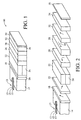
- an optical assembly 10 is shown as including an array 12 of TEC fibers 13, 15 and 17 coupled to an array of optical elements.
- the embodiment of Figs. 1 and 2 will be described as a three-port optical circulator, but this is not critical.
- the width of the array of optical elements as measured in a direction perpendicular to the length of the TEC fibers, accommodates a greater number of fibers, as will be described more fully below.
- the width approaches a minimum width for accomplishing the signal transfers for which the optical assembly is designed.
- the TEC fiber array 12 preferably has a pitch of less than 300 ⁇ m, but this is not critical. Presently, the minimum pitch is 125 ⁇ m, with an optimal pitch of 250 ⁇ m.
- the TEC fibers are preferably seated on a silicon wafer 14, which may be coated with a material to fix the fibers in position. The proper alignment may be achieved by forming V-shaped grooves in the silicon wafer. The structure of an individual TEC fiber will be described below with reference to Fig. 5. TEC fibers are commercially available from Sumitomo Osaka Cement Co., Ltd.
- Propagation of light from one of the TEC fibers in the array 12 into the array of optical elements will be described as propagation in a forward direction. The propagation continues forwardly until a mirror 16 reflects the light. Rearward propagation is defined as travel of light from the mirror toward the array 12 of TEC fibers.
- the first and second optical elements 18 and 20 form a walk-off crystal pair.
- the crystal pair operates to separate an input beam into orthogonal polarization components. With a walk-off direction of ⁇ 45°, a spatial separation of the polarization components is achieved.
- the thickness of the walk-off crystal pair may be only 0.885 mm in order to achieve the desired vertical separation.
- the material of the walk-off crystals 18 and 20 may be rutile (titanium dioxide-TiO 2 ) or yttrium vanadate (YVO 4 ).
- the preferred material is rutile, since it provides a greater refractive index. Consequently, rutile has a smaller in vacuo path length for a desired walk-off distance. A smaller path length results in less lateral spreading of the polarization components as they pass through the walk-off crystals.
- the desired walk-off distance by the crystal pair 18 and 20 determines the thickness of the two elements.
- the walk-off crystals must vertically separate the polarization components such that one polarization component passes through an upper half-wave plate 22 and the other polarization component passes through a lower half-wave plate 24.
- the operations of the half-wave plates with a 45° Faraday rotator 26 place the polarization states of the polarization components in a parallel relationship.
- the optical axis of the upper plate 22 is -45°
- the optical axis of the lower plate 24 is 0°.
- the optical axis of the upper plate 22 is 0° and the optical axis of the lower plate is +45°.
- the Faraday rotator provides 45° counterclockwise rotation or 45° clockwise rotation.
- the next element in the forward direction of light propagation is a walk-off crystal 28. Since the polarization states of the two polarization components are in a parallel relationship, the walk-off crystal 28 uniformly affects the vertically separated polarization components. As shown in Fig. 2, a walk-off direction 30 is perpendicular to the propagating light.
- the walk-off distance is preferably equal to the core-to-core pitch of the TEC fibers in the array 12.
- the preferred material for forming the walk-off crystal is rutile.
- the crystal thickness, as measured parallel to the direction of light propagation should be approximately ten times the pitch of the TEC fibers in the array 12.
- the laterally displaced and vertically separated polarization components then enter another quarter-wave plate 32 having an optical axis of either +45° or -45°.
- the functions of the three optical elements 32, 34 and 16 at the rearward end of the assembly 10 are (1) to focus, (2) to reflect, and (3) to change the polarization states of the two polarization components so that the reflected light is not shifted a second time by the walk-off crystal 28. While Figs. 1 and 2 illustrate an embodiment in which the three functions are achieved by three optical elements, this is not critical.
- the optical element 32 may be a quarter-wave plate and the mirror 16 may be fabricated to include an array of concave features that are aligned and dimensioned to independently focus the two polarization components of an input signal, thereby providing all three functions with only two optical elements.
- the three functions are achieved using a quarter-wave mirror having the focusing elements.
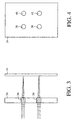
- the focusing is achieved using an array of microlenses formed in a glass substrate 34.
- a side view of the glass substrate and mirror 16 is shown in Fig. 3, while a forward-looking view of the glass substrate is shown in Fig. 4.
- Four microlenses 36, 38, 40 and 42 may be provided by diffusing ions through a photolithographic mask into the glass substrate.
- Such microlens arrays are commercially available from NSG America, Inc.
- a swelled curvature may be created on the surface of each microlens 36-42 to increase the numerical aperture, if necessary.
- the microlens array improves the coupling efficiency for transferring input light signals from one TEC fiber 13, 15 and 17 in the array 12 to an adjacent TEC fiber.
- the ion implantation which forms the microlenses 36, 38, 40 and 42 is applied at the forward face of the glass substrate 34.
- Each microlens may then be fabricated to provide a focal length that is equal to the distance between the forward face and the surface of the mirror 16.
- the beam diverges as it approaches a microlens.
- the beam energy is converged by the microlens and is reflected by the mirror.
- the rearwardly reflected beam is divergent, until the microlens refocuses the beam as it propagates rearwardly for output through the appropriate TEC fiber.
- the lenses provide approximately four-to-one imaging for efficient optical coupling to the appropriate TEC fiber.
- the microlenses 36 and 38 provide focusing for the two polarization components that are formed by separating a light signal input from a first TEC fiber 13 in the array 12.
- the vertical distance between the two microlenses 36 and 38 is determined by the walk-off in the vertical direction during the propagation of the input light beam through the walk-off crystal pair 18 and 20.
- the distance between horizontally adjacent microlenses, e.g. 36 and 40 is determined by the pitch of the TEC fibers in the array 12.
- the pitch of the fibers is 250 ⁇ m, so that the spacing between the optical axis of the microlens 36 and the optical axis of the microlens 40 is also 250 ⁇ m.
- the microlenses 36 and 38 are utilized when an input signal is received from the first TEC fiber 13 in the array 12.
- the optical elements in the assembly 10 couple the input signal from the first fiber to an adjacent TEC fiber.
- the second TEC fiber is the center fiber 15. If the center fiber is used to input a light signal, the signal is divided into polarization components which are focused using the microlenses 40 and 42. The light signal from the center fiber is output via the third fiber 17 in the array.
- the total number of microlenses in the array will be equal to 2n-2, where n is the number of TEC fibers in the array.
- Fig. 4 illustrates the microlenses 36-42 as being formed in the glass substrate 34
- the microlenses may be formed in the mirror 16 of Fig. 3, as noted above. That is, Fig. 4 may be the forward surface of the mirror 16.
- the positions of the concave surface features in the mirror would be identical to the positions described with reference to the glass substrate 34.
- the contour of the surface features should be designed to image an input signal at the appropriate output TEC fiber.
- the mirror may be a glass substrate with a high reflectivity coating (e.g. gold) on the rearward face.
- the glass substrate could include the ion-formed microlenses which provide the required difference in refractive index for focusing each of the polarization components.
- a large-area lens may be substituted for the glass substrate 34 having the array of microlenses 36-42.
- this is not preferred.
- the use of a focusing element is not required.
- commercially available TEC fibers require focusing in order to achieve optical coupling with an acceptable level of insertion loss. An acceptable level is between 1 dB and 2 dB.
- the commercially available TEC fibers have a mode-field diameter (MFD) of no greater than 45 ⁇ m. If TEC fibers having a larger MFD, such as 100 ⁇ m, become available, the fiber-to-fiber insertion loss will be reduced to an acceptable level without the use of an imaging lens.
- MFD mode-field diameter
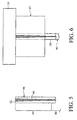
- Each fiber is a thermally diffused, expanded-core (TEC) single-mode optical.fiber.
- the TEC fiber 44 in Figs. 5 and 6 has an optical core 46 with a constant diameter along a major portion 48 of the fiber.
- the major portion 48 is truncated in Fig. 5.
- the diameter of the optical fiber progressively expands to reach a major diameter at a surface 52 that abuts the first walk-off crystal 18 of the array of optical elements.
- the expansion factor of the core is typically in the range of 2 to 5, and the expansion region typically has a length in the range of 4 to 6 mm.
- the expanded optical core 46 at the first end 50 of the fiber 44 reduces the angle at which light emitted from the surface 52 diverges laterally, as compared to conventional optical fibers.
- the reduction in the angle at which the light diverges is approximately equal to the expansion factor.
- the reduced lateral spreading of the light beam emitted from the TEC fiber 44 enables the spacing between the centers of adjacent TEC fibers to be substantially reduced.
- the spacing is reduced to the distance corresponding to the outside diameter of the optical fibers. This places the outside surface of the optical fibers in contact with one another, as shown in Fig. 1. Minimizing the spacing between light beams provides a high density of input/output ports to the optical assembly of Fig. 1. This enables a reduction in the size and the cost of the assembly.
- the material coating the optical core is removed in order to facilitate seating of the fiber within a V-groove of a silicon wafer.
- a V-groove of a silicon wafer Such an embodiment is shown in Figs. 15 and 16.
- the fiber cores 80, 82, 84, 86 and 88 are spaced apart from each other.
- a forward face of the first walk-off crystal 18 is shown as having three relevant locations 54, 56 and 58.
- the three locations correspond to the axes of the three TEC fibers 13, 15 and 17 in the array 12 of Fig. 1.
- the location 56 corresponds to the fiber axis of a bidirectional TEC fiber that is optically coupled to the first TEC fiber 13 of location 54 to receive an input signal and is coupled to the third TEC fiber 17 at location 58 to transmit a light signal to the third TEC fiber.
- the fibers are optically isolated with respect to all other light propagation. However, other embodiments are anticipated.
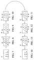
- an input signal from the first TEC fiber is represented by two polarization components that intersect at location 54.
- one of the polarization components is shown as being thicker than the other polarization component.
- the first operation of the optical elements is to spatially separate the two polarization components. This operation is performed by the pair of walk-off crystals 18 and 20. Consequently, at the forward faces of the upper and lower half-wave plates 22 and 24, the two polarization components are vertically separated. This is represented in Fig. 8 at locations 60 and 62.
- the two polarization components at locations 60 and 62 are still in orthogonal relationship, but have been vertically separated to align one polarization component for propagation through the upper half-wave plate 22 and align the other polarization component for propagation through the lower half-wave plate 24.
- a second operation of the optical assembly 10 is to align the polarization states of the two polarization components into an orientation for lateral displacement of the components by the walk-off crystal 28.
- the realigned polarization components at the forward face of the walk-off crystal 28 are shown in Fig. 9.
- the combination of the two half-wave plates 22 and 24 and the 45° Faraday rotator 26 provides a clockwise rotation of 45° for the upper polarization component and a counterclockwise rotation of 45° for the lower polarization component. Therefore, the polarizations are the parallel states at the forward face of the walk-off crystal 28, as shown in Fig. 9.
- the polarization components are displaced in a horizontal walk-off direction by a walk-off separation equal to the pitch of TEC fiber array 12.
- the polarization components have been shifted from locations 60 and 62 to locations 64 and 66.
- the walk-off crystal 28 that provides the horizontal displacement equal to the pitch of the TEC fiber array is non-reciprocal.
- the polarization states of the polarization components are changed from horizontal to vertical.
- the optical elements 32, 34 and 16 cooperate to provide a quarter-wave mirror lens assembly. The result is shown at the rearward face of the walk-off crystal 28 in Fig. 11. Comparing the forwardly propagating polarization components at the forward face of the crystal 28 in Fig. 11 with the rearwardly propagating polarization components at the rearward face of the crystal 28 in Fig. 11, the components have been displaced laterally and have rotated polarization states.
- the non-reciprocal walk-off crystal 28 does not affect propagation of the polarization components through the crystal. Consequently, the polarization components reach the rearward face of the Faraday rotator 26 in the states and positions shown in Fig. 12.
- the Faraday rotator 26 and the two half-wave plates 22 and 24 return the two states of the polarization components into the original orthogonal relationship.
- the polarization component at location 64 passes through the Faraday rotator and the upper half-wave plate and is consequently rotated 45° clockwise.
- the propagation of the lower polarization component through the Faraday rotator and the lower half-wave plate causes 45° counterclockwise rotation of the polarization state.
- the 45° walk-off crystal pair formed by optical elements 18 and 20 recombine the two polarization components.
- the output light signal is aligned with the location 56 of the center TEC fiber when the polarization components reach the forward face of the first walk-off crystal 18.
- the input of the light signal at location 54 by the first TEC fiber is coupled to the center TEC fiber in Fig. 14 at location 56.
- An identical operation occurs at the center TEC fiber as an input fiber for the third TEC fiber at location 58.
- the polarization components will follow the same operations for input signals from the center TEC fiber, but will be at positions to the right of the polarization components illustrated in Figs. 7-14.
- the optical properties of the elements to not allow reverse coupling. That is, the assembly provides a selective optical coupling and a selective optical isolation of the three fibers.
- a preferred method for properly aligning the TEC fibers is described with reference to Figs. 15 and 16.
- a semiconductor substrate such as a silicon wafer 68, is etched to form V-shaped grooves 70, 72, 74, 76 and 78.
- Conventional integrated circuit fabrication techniques may be utilized.
- the grooves may be formed photolithographically, using a mask to define the grooves and using a chemical etchant. While not critical, the angle of one wall of a groove relative to the other wall is preferably 70.5°.
- TEC fiber cores 80, 82, 84, 86 and 88 without coating material are then placed within the grooves.
- the silicon processing enables a precise center-to-center spacing of the fiber cores. Tolerances of less than 1 micron are achieved.
- a second silicon wafer 90 having a corresponding array of V-shaped grooves is fixed to the lower silicon wafer 68 by a layer of adhesive 92.
- the use of an adhesive layer is not critical.
- wafer bonding may be used to attach the two silicon wafers.
- Silicon V-groove alignment of single-mode fibers and multi-mode fibers is known in the art, and assemblies of the type shown in Fig. 16 are commercially available.
- An advantage of silicon micromachining to provide sub-micron tolerances for TEC fiber alignment is that all of the fibers are brought into registration with optical elements by properly aligning one of the fibers.
- the three TEC fibers in the array 12 will have a known fiber-to-fiber pitch that can be reliably used to determine the walk-off distances for optical elements 18, 20 and 28 and the pitch of the microlenses 36, 38, 40 and 42.
- a number of the optical assemblies 10 of Fig. 1 may be fabricated in bulk and dissected to form multiple assemblies only after the two TEC fibers at the opposite ends of the array are properly aligned to the optical elements. By ensuring that the two fibers at the opposite ends are properly positioned, the interior fibers are simultaneously aligned with the associated optical elements, such as the microlenses.
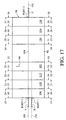
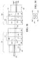
- Figs. 17 and 18 show a side view and a plan view of a second embodiment of a compact optical assembly 94 that utilizes an interior lens element 96.
- the assembly of Figs. 17 and 18 is a three-port optical circulator that does not include the mirror element of Fig. 1. Instead, two complementary input/output (I/O) assemblies 98 and 100 are at opposite ends of the three-port optical circulator. Between the two I/O assemblies are a perpendicular walk-off crystal 102 and the lens element 96. The perpendicular walk-off crystal laterally displaces light propagating through the circulator in the forward direction, but does not laterally displace light propagating in the reverse direction. In Figs. 17 and 18, the forward direction is defined as the propagation from the first I/O assembly 98 to the second I/O assembly 100.
- the optical axis of the lens element 96 defines the optical axis 104 of the circulator 94.
- PORT 2 is a TEC fiber through which the optical circulator receives a light beam Y.
- PORT 3 is a TEC fiber through which the optical circulator receives a light beam Z.
- the light beams Y and Z are located on the optical axis 104.
- PORT 1, through which the optical circulator receives a light beam X, is displaced laterally from the optical axis. For example, the lateral displacement from the optical axis may be less than approximately 200 ⁇ m.
- the optical circulator 94 receives the two input light beams X and Y via PORT 1 and PORT 2, respectively.
- the light beam X is transmitted to PORT 3, while the light beam Y is transmitted to a location laterally displaced from PORT 3.
- the optical circulator receives the input light beam Z via PORT 3 and transmits the light beam to PORT 2.
- the first I/O assembly 98 includes a walk-off crystal 106, split half-wave plates 108 and 110, and a Faraday rotator 112.
- the split half-wave plates 108 and 110 and the Faraday rotator 112 operate as a split polarization rotator 114 arranged along the optical axis in the forward direction of beam propagation.
- the half-wave plate 108 is referred to herein as the positive half-wave plate, while the adjacent plate 110 will be referred to as the negative half-wave plate.
- the two plates are joined at a line of attachment 116.
- the second I/O assembly 100 is the complement of the first I/O assembly 98.
- a walk-off crystal 118 receives an input signal from the TEC fiber of PORT 3.
- a split polarization rotator 120 is comprised of a positive half-wave plate 122, a negative half-wave plate 124, and a Faraday rotator 126.
- the operations of the split polarization rotators are dependent upon the direction of beam propagation.
- the rotational direction is either 0° or 90°, depending upon whether the light is passing through the positive half-wave plate 108 or the negative half-wave plate 110 and depending upon whether the light is propagating in the forward direction or the rearward direction.
- the Faraday rotator 112 is selected to rotate the direction of polarization of light passing through the optical circulator 94 in the forward direction clockwise by 45°.
- the Faraday rotator is a non-reciprocal device, so it rotates the direction of polarization of light passing through the first split polarization rotator 114 in the rearward direction counterclockwise by 45°.
- the half-wave plates 108 and 110 of the first split polarization rotator 114 are reciprocal devices.
- the positive half-wave plate 108 has an optical axis, indicated by line 128, aligned at +22.5° relative to the line of attachment 116.
- the negative half-wave plate 110 has an optical axis, indicated by line 130, aligned at -22.5° relative to the line of attachment.
- the positive half-wave plate effectively rotates a polarization component that is parallel or perpendicular to the line of attachment 116 by 45° counterclockwise about the direction of travel of the light. This can be seen by comparing Figs. 20 (left-hand half) and 21. Figs. 19-27 will be described more fully below.
- the negative half-wave plate 110 effectively rotates a polarization component that is parallel or perpendicular to the line of attachment 116 by 45° clockwise about the direction of travel of the light. This can be seen by comparing Figs. 20 (right-hand half) and 21.
- the operation of the second split polarization rotator 120 is similar to that of the first polarization rotator and will not be described separately.
- the positive half-wave plate 122 has an optical axis 132 that is offset by +22.5°, while the negative half-wave plate 124 has an optical axis 134 that is offset by -22.5°.
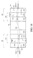
- Figs. 19-27 illustrate polarization components of light beams X and Y at various locations during forward propagation through the optical circulator of Fig. 17.
- the light beams X and Y are shown at the forward face of the walk-off crystal 106.
- the light beam X is shown as having an orthogonal polarization component O1 indicated by a long thick bar, and a parallel polarization component P1, indicated by a short thick bar.
- the light beam Y is shown as having an orthogonal polarization component O2, indicated by a long thin bar, and a parallel polarization component P2, indicated by a short thin bar.
- the orthogonal polarization components O1 and O2 are the polarization components of the light beams X and Y that are perpendicular to the walk-off direction 136 of the walk-off crystal 106 of the first I/O assembly 98.
- the parallel polarization components P1 and P2 are the polarization components of the light beams X and Y that are parallel to the walk-off direction 136.
- the parallel polarization components P2 and P1 are respectively located at the displaced locations 138 and 140, as shown in Fig. 20.
- the displacement is relative to the optical axis 104 of Figs. 17 and 18.
- the locations 138 and 140 are also displaced relative to locations 142 and 144 of the orthogonal polarization components O2 and O1 by the walk-off distance of the walk-off crystal 106.
- the walk-off crystals may be made of rutile. The walk-off distance will be dependent upon the thickness of the crystal.
- the line of attachment 116 of the positive and negative half-wave plates 108 and 110 is displaced laterally from the optical axis 104 in the walk-off direction 136 of the walk-off crystal 106 by approximately one-half of the walk-off distance. Consequently, as shown in Fig. 20, the orthogonal polarization components O1 and O2 enter the positive half-wave plate 108 and the parallel polarization components P1 and P2 enter the negative half-wave plate 110, with the locations 138, 140, 142 and 144 being symmetrically arranged relative to the line of attachment 116.
- Fig. 22 illustrates the polarization components as they enter the perpendicular walk-off crystal 102 from the split polarization rotator 114.
- the first split polarization rotator 114 rotates the direction of polarization of only the parallel polarization components P1 and P2 in order to set the direction of polarization of all four polarization components parallel to the walk-off direction 146 of the perpendicular walk-off crystal 102.
- the perpendicular walk-off crystal displaces each of the polarization components in the walk-off direction by the walk-off distance determined by the thickness of the crystal.
- the walk-off distance should be equal to the spacing between the light beams X and Y in Fig. 19. Consequently, the perpendicular walk-off crystal laterally displaces the orthogonal polarization component O1 of the light beam X to a position corresponding to the optical axis 104 of the light beam Y.
- the perpendicular walk-off crystal also laterally displaces the parallel component P1 of the light beam X to the displaced location 138 previously occupied by the parallel component P2.
- the polarization components O2 and P2 are likewise shifted in the walk-off direction 146 by the walk-off distance. As shown in Fig. 23, polarization component O2 is shifted to displaced location 148 and the polarization component P2 is shifted to the displaced location 150.
- the lens element 96 may be a single gradient-index (GRIN) lens or may be a lens array of the type described with reference to Fig. 3.
- the lens or lenses reconverge the individual polarization components, which diverge as they pass through the optical circulator 94.
- the focal length of each lens and its spacing from the forward face of the second I/O assembly 100 forms an image on the adjacent element.
- the adjacent element In the forward direction, the adjacent element is the Faraday rotator 126, while in the rearward direction of propagation, the adjacent element is the perpendicular walk-off crystal 102.
- the lens 96 inverts the positions of the polarization components O1, P1, O2 and P2 about the optical axis 104. Since the orthogonal polarization component O1 lies on the optical axis, the lens leaves the position of this polarization component unchanged.
- the axis 152 of PORT 3 coincides with the optical axis, so the lens leaves the orthogonal polarization component O1 aligned with PORT 3.
- the lens inverts the position of the orthogonal polarization component O2 about the optical axis to the position 144 corresponding to the axis 154 of the light beam X, and inverts the positions of the parallel polarization components P1 and P2 about the optical axis to displaced locations 156 and 158, as shown in Fig. 24.
- Fig. 24 shows the polarization components as they enter the second I/O assembly in the forward direction.
- the Faraday rotator 126 causes clockwise rotation of the polarization components. The rotation is continued by the positive half-wave plate 122 in Fig. 25, but the negative half-wave plate 124 returns the orthogonal components O1 and O2 to the direction shown in Fig. 24.
- the polarization components passing through the optical circulator 94 in the forward direction propagate through the second split polarization rotator 120 in the opposite arrangement of the propagation through the first split polarization rotator 114. Consequently, the direction of polarization of the orthogonal components O1 and O2 is unchanged by the propagation through the Faraday rotator 126 and the negative half-wave plate 124.
- the direction of polarization of the parallel components P1 and P2 is rotated through 90° by passage through the Faraday rotator 126 and the positive half-wave plate 122.
- Fig. 26 shows the polarization components as they enter the walk-off crystal 118 from the second split polarization rotator 120.
- the parallel polarization components P1 and P2 are parallel to the walk-off direction 160 of the walk-off crystal 118.
- the walk-off distance is selected to be equal to the distance between locations 142 and 156. Consequently, the parallel polarization components P1 and P2 are shifted into alignment with the corresponding orthogonal polarization components O1 and O2.
- the parallel polarization component P1 of the light beam X is overlaid on the orthogonal polarization component O1 of the light beam X at the location of the axis of PORT 3, and the parallel polarization component P2 of the light beam Y is overlaid on the orthogonal polarization component O2 of the light beam Y at the location 144 of the axis 154, laterally displaced from PORT 3.
- the parallel polarization component P2 of the light beam Y is overlaid on the orthogonal polarization component O2 of the light beam Y at the location 144 of the axis 154, laterally displaced from PORT 3.
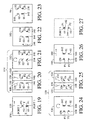
- Figs. 28-36 show the polarization component of the light beam Z and a spurious light beam S at various points in the optical circulator, as indicated by section lines 28-28 through 36-36 in Fig. 17.
- the light beam Z is an input beam from PORT 3, which is a TEC fiber.
- the spurious light beam S is the same beam that is illustrated in Fig. 27 as being misaligned with PORT 3 in order to optically isolate PORT 2 from PORT 3 with respect to light propagating in the forward direction.
- Fig. 28 shows the light beams Z and S as the beams enter the second I/O assembly 100.
- the light beam Z enters the second I/O assembly at location 142, which is coaxial with the axis 152 of PORT 3.
- the light beam Z has an orthogonal polarization component O1, indicated by a long thick bar, and a parallel polarization component P1, indicated by a short thick bar.
- the spurious light beam includes an orthogonal polarization component 02, indicated by a long thin bar, and a parallel polarization component P2, indicated by a short thin bar.
- the orthogonal polarization components O1 and O2 are perpendicular to the walk-off direction 160 and therefore propagate through the crystal without deviation.
- the parallel polarization components P1 and P2 are parallel to the walk-off direction of the crystal, so that the components are deviated by the distance of the walk-off distance of the crystal.
- Fig. 29 shows the polarization components as they enter the positive and negative half-wave plates 122 and 124 of the second split polarization rotator 120.
- the parallel polarization components P1 and P2 are respectively located at the displaced locations 164 and 166 to the right of a line of attachment 162 of the two half-wave plates 122 and 124.
- the line of attachment 162 is displaced laterally from the optical axis of the optical circulator by a distance of approximately one-half of the walk-off distance of the crystal 118. This causes the orthogonal polarization components to enter the negative half of the split polarization rotator, and the parallel polarization components to enter the positive half of the split polarization rotator.
- the locations 142, 144, 164 and 166 are symmetrically disposed relative to the line of attachment 162.
- the second split polarization rotator 120 rotates the polarization direction of the orthogonal polarization components O1 and O2 by 90°, but does not affect the polarization direction of the parallel polarization components P1 and P2. Consequently, the polarization components have a common direction as they enter the lens element 96 that preferably includes an array of microlenses.
- the lens element 96 inverts the positions of the polarization components O1, P1, O2 and P2 about the optical axis of the circulator. Since the orthogonal polarization component O1 lies on the optical axis 104 of the circulator, the lens element leaves the position of O1 unchanged, as shown in Fig. 32.
- the lens element 96 Since the axis 168 of PORT 2 in Fig. 17 coincides with the optical axis 104, the lens element 96 leaves this polarization component aligned with PORT 2. However, the lens element inverts the positions of the orthogonal polarization component 02 and the parallel polarization components P1 and P2 to the displaced locations 170, 172 and 174, respectively.
- the polarization components O1, O2, P1 and P2 are equally rotated by the Faraday rotator 112 of the first split polarization rotator 114, as shown in Fig. 34.
- the orthogonal polarization components O1 and O2 pass through the positive half-wave plate 108, causing further counterclockwise rotation of the polarization direction.
- the parallel components P1 and P2 have polarization directions that are rotated in the clockwise direction, returning the components to the direction shown in Fig. 35. That is, the first split polarization rotator 114 causes 90° rotation of the orthogonal components, but leaves the parallel components unchanged.
- Fig. 35 shows the polarization components as they enter the walk-off crystal 106 from the first split polarization rotator 114.
- the orthogonal polarization components O1 and O2 are set in the polarization direction perpendicular to that of the parallel polarization components P1 and P2.
- the parallel polarization components remain parallel to the walk-off direction 136 of the walk-off crystal 106. Consequently, as shown in Fig. 36, the crystal deflects the parallel polarization components to overlay the associated orthogonal polarization components.
- the light beam Z is thereby aligned with PORT 2.
- the spurious light beam S is aligned with displaced location 170, so that the spurious light beam is optically isolated from the two TEC fibers at PORT 1 and PORT 2.
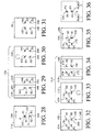
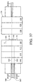
- FIG. 37 and 38 Another embodiment is shown in Figs. 37 and 38. Many of the optical elements of the circulator 176 of Figs. 37 and 38 are identical to optical elements in the embodiment of Figs. 17 and 18. Therefore, many of the reference numerals have been duplicated.
- the illustration of the optical circulator 176 has been expanded to show the first I/O assembly 178 as including the two TEC fibers 180 and 182 that are precisely aligned on a silicon V-groove member 184 of the type described with reference to Figs. 15 and 16.
- the second I/O assembly 186 is now illustrated as including the third TEC fiber 188 formed on a silicon V-groove member 190.
- the embodiment illustrated in Figs. 37 and 38 includes the array 192 of microlenses.
- the microlens array 192 comprises four converging lenses 194, 196, 198 and 200.
- the array is located adjacent to the rearward face of the perpendicular walk-off crystal 102.
- the perpendicular walk-off crystal may be spaced from the first I/O assembly 178 and the microlens array may be located adjacent to the forward face of the perpendicular walk-off crystal.
- Microlenses having a spacing of 250 ⁇ m between the optical axes of adjacent lenses are available from Nippon Sheet Glass Co.
- the I/O assemblies may be easily modified to double the spacing between the optical axes 104 and 202 and to double the walk-off distance of the walk-off crystals 106 and 118.
- each of the four microlenses 194, 196, 198 and 200 in the microlens array is centered on the axis of one of the polarization components O1, O2, P1 and P2 as the polarization components propagate to the microlens array.
- the focal length of the lenses in the array, and the spacing from the ends of the first and second TEC fibers 180 and 182 to the end of the third TEC fiber 188, are selected so that the microlenses form an image of PORT 1 at PORT 3 and form an image of PORT 3 at PORT 2.
- the various elements of the optical circulator 176 that are identical to elements of the optical circulator 94 of Fig. 17 operate in the manner described above, and the description will not be repeated.
- the significant difference is that the lens element, i.e., the microlens array 192, does not invert the polarization components in the manner described with reference to Figs. 17 and 18. Rather, the polarization components propagate linearly through the lens element in the manner described with reference to Figs. 3 and 4.
Landscapes
- Physics & Mathematics (AREA)
- General Physics & Mathematics (AREA)
- Optics & Photonics (AREA)
- Nonlinear Science (AREA)
- Engineering & Computer Science (AREA)
- Power Engineering (AREA)
- Optical Couplings Of Light Guides (AREA)
Applications Claiming Priority (2)
| Application Number | Priority Date | Filing Date | Title |
|---|---|---|---|
| US08/915,525 US5930418A (en) | 1997-02-25 | 1997-08-15 | Optical assembly and method based on TEC fibres |
| US915525 | 1997-08-15 |
Publications (3)
| Publication Number | Publication Date |
|---|---|
| EP0898185A2 EP0898185A2 (en) | 1999-02-24 |
| EP0898185A3 EP0898185A3 (en) | 2001-04-25 |
| EP0898185B1 true EP0898185B1 (en) | 2002-08-21 |
Family
ID=25435898
Family Applications (1)
| Application Number | Title | Priority Date | Filing Date |
|---|---|---|---|
| EP98109846A Expired - Lifetime EP0898185B1 (en) | 1997-08-15 | 1998-05-29 | Optical assembly and method based on tec fibers |
Country Status (5)
| Country | Link |
|---|---|
| US (1) | US5930418A (enExample) |
| EP (1) | EP0898185B1 (enExample) |
| JP (1) | JPH11133261A (enExample) |
| AU (1) | AU743545B2 (enExample) |
| DE (1) | DE69807298T2 (enExample) |
Families Citing this family (19)
| Publication number | Priority date | Publication date | Assignee | Title |
|---|---|---|---|---|
| US6048103A (en) * | 1995-12-21 | 2000-04-11 | Kyocera Corporation | Polarization independent optical isolator with integrally assembled birefringent crystal element and Faraday rotator |
| US6239900B1 (en) * | 1997-09-19 | 2001-05-29 | Nz Applied Technologies Corp. | Reflective fiber-optic isolator |
| US6044187A (en) * | 1998-04-01 | 2000-03-28 | Duck; Gary S. | Multi-port fiber optical device |
| US6075642A (en) * | 1998-06-18 | 2000-06-13 | Hewlett-Packard Company | Multi-port optical isolator |
| US6064522A (en) * | 1998-06-23 | 2000-05-16 | Lucent Technologies Inc | Miniature mass producible non-reciprocal devices |
| US6078716A (en) * | 1999-03-23 | 2000-06-20 | E-Tek Dynamics, Inc. | Thermally expanded multiple core fiber |
| US6263131B1 (en) * | 1999-07-02 | 2001-07-17 | Nortel Networks (Photonics) Pty Ltd. | Reflective non-reciprocal optical device |
| US6236506B1 (en) * | 1999-09-23 | 2001-05-22 | Avanex Corporation | Reflection-type optical circulation utilizing a lens and birefringent plates |
| US6560015B1 (en) * | 1999-09-23 | 2003-05-06 | Avanex Corporation | High-isolation dense wavelength division multiplexer utilizing birefringent plates and a non-linear interferometer |
| US6853488B1 (en) * | 1999-09-23 | 2005-02-08 | Avanex Corporation | Reflection-type optical circulator utilizing a lens and birefringent plates |
| US6532316B1 (en) * | 1999-11-10 | 2003-03-11 | Avanex Corporation | Bi-directional polarization-independent optical isolator |
| CN1133084C (zh) * | 2000-03-24 | 2003-12-31 | 信息产业部武汉邮电科学研究院 | 梳状分波方法 |
| TW440712B (en) * | 2000-06-07 | 2001-06-16 | Ind Tech Res Inst | Optical circulator |
| US6563641B2 (en) * | 2000-06-23 | 2003-05-13 | Cirvine Corporation | Fold interleaver |
| JP2003270681A (ja) * | 2002-03-19 | 2003-09-25 | Fdk Corp | 反射型光スイッチ |
| CN101401021B (zh) * | 2006-03-09 | 2010-10-27 | 并木精密宝石株式会社 | 反射型光循环器 |
| US7945158B2 (en) * | 2006-08-18 | 2011-05-17 | Tellabs Operations, Inc. | Transponder-less verification of the configuration of an optical network node |
| WO2015081806A1 (zh) * | 2013-12-04 | 2015-06-11 | 匠研光学科技(上海)有限公司 | 一种与波长和温度无关的法拉第旋转镜 |
| US10191194B2 (en) * | 2014-11-05 | 2019-01-29 | Rochester Institute Of Technology | Spectral target for macroscopic and microscopic reflectance imaging |
Family Cites Families (22)
| Publication number | Priority date | Publication date | Assignee | Title |
|---|---|---|---|---|
| JPS6049297B2 (ja) * | 1977-05-31 | 1985-11-01 | 日本電気株式会社 | 光アイソレ−タ |
| US4737004A (en) * | 1985-10-03 | 1988-04-12 | American Telephone And Telegraph Company, At&T Bell Laboratories | Expanded end optical fiber and associated coupling arrangements |
| US4974944A (en) * | 1988-07-21 | 1990-12-04 | Hewlett-Packard Company | Optical nonreciprocal device |
| US5151955A (en) * | 1990-06-20 | 1992-09-29 | Kabushiki Kaisha Shinkosha | Optical isolator |
| US5237445A (en) * | 1990-11-30 | 1993-08-17 | Shimadzu Corporation | Optical isolator |
| DE69121176T2 (de) * | 1990-12-17 | 1997-01-09 | Nippon Telegraph & Telephone | Optischer Zirkulator |
| CA2080904A1 (en) * | 1991-02-20 | 1992-08-21 | Shigeru Hirai | Optical isolator |
| JPH04333808A (ja) * | 1991-05-10 | 1992-11-20 | Nec Corp | 光半導体モジュール |
| US5428477A (en) * | 1991-06-14 | 1995-06-27 | Tokin Corporation | Optical isolator operating independent of polarization of an incident beam |
| JP3160319B2 (ja) * | 1991-07-25 | 2001-04-25 | 株式会社信光社 | 光アイソレータ |
| JP2757093B2 (ja) * | 1992-04-20 | 1998-05-25 | 富士電気化学株式会社 | 無偏波分散型光アイソレータ |
| US5319483A (en) * | 1992-12-04 | 1994-06-07 | Williams Telecommunications Group, Inc. | Polarization independent low cross-talk optical circulator |
| JPH08505961A (ja) * | 1993-01-21 | 1996-06-25 | イー−テック・ダイナミックス・インコーポレイテッド | 偏光モード分散の低い光学装置 |
| US5493440A (en) * | 1993-10-19 | 1996-02-20 | Matsushita Electric Industrial Co., Ltd. | Optical isolator and optical fiber amplifier |
| US5471340A (en) * | 1994-01-07 | 1995-11-28 | Jds Fitel Inc. | Reflective optical non-reciprocal devices |
| JPH0821924A (ja) * | 1994-07-05 | 1996-01-23 | Fuji Elelctrochem Co Ltd | 複数伝送路を有する複数ポート光部品 |
| US5539574A (en) * | 1994-12-21 | 1996-07-23 | At&T Corp. | Optical isolator with fabry-perot ripple reduction |
| CA2148317C (en) * | 1995-05-01 | 1998-05-05 | Yihao Cheng | Optical circulator |
| AUPN714295A0 (en) * | 1995-12-14 | 1996-01-11 | Photonic Technologies Pty Ltd | Fibre optic circulator |
| US5825950A (en) * | 1996-05-13 | 1998-10-20 | Jds Fitel Inc. | Optical isolator |
| US5734763A (en) * | 1996-09-04 | 1998-03-31 | Hewlett-Packard Company | Compact two-by-n optical components based on bierfringent walk-off crystals |
| US5706371A (en) * | 1996-12-03 | 1998-01-06 | E-Tek Dynamics, Inc. | Optical isolator array device |
-
1997
- 1997-08-15 US US08/915,525 patent/US5930418A/en not_active Expired - Lifetime
-
1998
- 1998-05-29 DE DE69807298T patent/DE69807298T2/de not_active Expired - Lifetime
- 1998-05-29 EP EP98109846A patent/EP0898185B1/en not_active Expired - Lifetime
- 1998-06-05 AU AU69956/98A patent/AU743545B2/en not_active Ceased
- 1998-08-04 JP JP10232297A patent/JPH11133261A/ja not_active Withdrawn
Also Published As
| Publication number | Publication date |
|---|---|
| US5930418A (en) | 1999-07-27 |
| DE69807298T2 (de) | 2003-04-17 |
| EP0898185A3 (en) | 2001-04-25 |
| DE69807298D1 (de) | 2002-09-26 |
| AU6995698A (en) | 1999-02-25 |
| JPH11133261A (ja) | 1999-05-21 |
| AU743545B2 (en) | 2002-01-31 |
| EP0898185A2 (en) | 1999-02-24 |
Similar Documents
| Publication | Publication Date | Title |
|---|---|---|
| EP0898185B1 (en) | Optical assembly and method based on tec fibers | |
| EP0965867B1 (en) | Multi-port optical circulator utilizing imaging lens and correction optical element | |
| US5740288A (en) | Variable polarization beam splitter, combiner and mixer | |
| US5588078A (en) | Non-reciprocal optical waveguide coupling device | |
| JP4397999B2 (ja) | マルチポート光学アセンブリに対する光ファイバの位置合わせ方法 | |
| US6590706B1 (en) | Optical circulators using beam angle turners | |
| US6249619B1 (en) | Optical isolator | |
| EP0786681A1 (en) | Polarization-independent optical isolator | |
| US6263131B1 (en) | Reflective non-reciprocal optical device | |
| KR20010089361A (ko) | 다중 포트 광섬유 순환기 | |
| CN110109270B (zh) | 光环形器 | |
| US5825950A (en) | Optical isolator | |
| JP3130499B2 (ja) | 3ポート光学サーキュレータ及びその製造方法 | |
| US6075642A (en) | Multi-port optical isolator | |
| US6310989B1 (en) | Fiber optical circulator | |
| US6438278B1 (en) | Fiber optical circulator | |
| US5991076A (en) | Optical circulator | |
| US6011649A (en) | Optical assembly and method for high performance coupling | |
| EP1113307A2 (en) | Optical circulator | |
| JP3368209B2 (ja) | 反射型光サーキュレータ | |
| US6366402B1 (en) | Method and system for providing an in-line optical circulator | |
| US6239900B1 (en) | Reflective fiber-optic isolator | |
| CN210488175U (zh) | 一种微型磁光光纤开关 | |
| WO1999012061A1 (en) | Multiport non-reciprocal optical device | |
| JP2524881Y2 (ja) | 光アイソレータ |
Legal Events
| Date | Code | Title | Description |
|---|---|---|---|
| PUAI | Public reference made under article 153(3) epc to a published international application that has entered the european phase |
Free format text: ORIGINAL CODE: 0009012 |
|
| AK | Designated contracting states |
Kind code of ref document: A2 Designated state(s): DE FR GB |
|
| AX | Request for extension of the european patent |
Free format text: AL;LT;LV;MK;RO;SI |
|
| PUAL | Search report despatched |
Free format text: ORIGINAL CODE: 0009013 |
|
| RIC1 | Information provided on ipc code assigned before grant |
Free format text: 7G 02B 6/28 A, 7G 02B 6/26 B, 7G 02F 1/095 B |
|
| AK | Designated contracting states |
Kind code of ref document: A3 Designated state(s): AT BE CH CY DE DK ES FI FR GB GR IE IT LI LU MC NL PT SE |
|
| AX | Request for extension of the european patent |
Free format text: AL;LT;LV;MK;RO;SI |
|
| RAP1 | Party data changed (applicant data changed or rights of an application transferred) |
Owner name: HEWLETT-PACKARD COMPANY, A DELAWARE CORPORATION |
|
| 17P | Request for examination filed |
Effective date: 20010529 |
|
| RAP1 | Party data changed (applicant data changed or rights of an application transferred) |
Owner name: AGILENT TECHNOLOGIES INC. |
|
| RAP1 | Party data changed (applicant data changed or rights of an application transferred) |
Owner name: AGILENT TECHNOLOGIES INC. A DELAWARE CORPORATION |
|
| GRAG | Despatch of communication of intention to grant |
Free format text: ORIGINAL CODE: EPIDOS AGRA |
|
| RAP1 | Party data changed (applicant data changed or rights of an application transferred) |
Owner name: AGILENT TECHNOLOGIES, INC. (A DELAWARE CORPORATION |
|
| 17Q | First examination report despatched |
Effective date: 20010919 |
|
| GRAG | Despatch of communication of intention to grant |
Free format text: ORIGINAL CODE: EPIDOS AGRA |
|
| GRAH | Despatch of communication of intention to grant a patent |
Free format text: ORIGINAL CODE: EPIDOS IGRA |
|
| AKX | Designation fees paid |
Free format text: DE FR GB |
|
| GRAH | Despatch of communication of intention to grant a patent |
Free format text: ORIGINAL CODE: EPIDOS IGRA |
|
| GRAA | (expected) grant |
Free format text: ORIGINAL CODE: 0009210 |
|
| AK | Designated contracting states |
Kind code of ref document: B1 Designated state(s): DE FR GB |
|
| PG25 | Lapsed in a contracting state [announced via postgrant information from national office to epo] |
Ref country code: FR Free format text: LAPSE BECAUSE OF NON-PAYMENT OF DUE FEES Effective date: 20020821 |
|
| REG | Reference to a national code |
Ref country code: GB Ref legal event code: FG4D |
|
| REF | Corresponds to: |
Ref document number: 69807298 Country of ref document: DE Date of ref document: 20020926 |
|
| EN | Fr: translation not filed | ||
| PLBE | No opposition filed within time limit |
Free format text: ORIGINAL CODE: 0009261 |
|
| STAA | Information on the status of an ep patent application or granted ep patent |
Free format text: STATUS: NO OPPOSITION FILED WITHIN TIME LIMIT |
|
| 26N | No opposition filed |
Effective date: 20030522 |
|
| PGFP | Annual fee paid to national office [announced via postgrant information from national office to epo] |
Ref country code: GB Payment date: 20060525 Year of fee payment: 9 |
|
| REG | Reference to a national code |
Ref country code: GB Ref legal event code: 732E |
|
| GBPC | Gb: european patent ceased through non-payment of renewal fee |
Effective date: 20070529 |
|
| PG25 | Lapsed in a contracting state [announced via postgrant information from national office to epo] |
Ref country code: GB Free format text: LAPSE BECAUSE OF NON-PAYMENT OF DUE FEES Effective date: 20070529 |
|
| PGFP | Annual fee paid to national office [announced via postgrant information from national office to epo] |
Ref country code: DE Payment date: 20170420 Year of fee payment: 20 |
|
| REG | Reference to a national code |
Ref country code: DE Ref legal event code: R071 Ref document number: 69807298 Country of ref document: DE |