EP0897784B1 - Carte à puce - Google Patents
Carte à puce Download PDFInfo
- Publication number
- EP0897784B1 EP0897784B1 EP98112833A EP98112833A EP0897784B1 EP 0897784 B1 EP0897784 B1 EP 0897784B1 EP 98112833 A EP98112833 A EP 98112833A EP 98112833 A EP98112833 A EP 98112833A EP 0897784 B1 EP0897784 B1 EP 0897784B1
- Authority
- EP
- European Patent Office
- Prior art keywords
- chip card
- component
- skin component
- card according
- plastic
- Prior art date
- Legal status (The legal status is an assumption and is not a legal conclusion. Google has not performed a legal analysis and makes no representation as to the accuracy of the status listed.)
- Expired - Lifetime
Links
Images

Classifications
-
- G—PHYSICS
- G06—COMPUTING; CALCULATING OR COUNTING
- G06K—GRAPHICAL DATA READING; PRESENTATION OF DATA; RECORD CARRIERS; HANDLING RECORD CARRIERS
- G06K19/00—Record carriers for use with machines and with at least a part designed to carry digital markings
- G06K19/06—Record carriers for use with machines and with at least a part designed to carry digital markings characterised by the kind of the digital marking, e.g. shape, nature, code
- G06K19/067—Record carriers with conductive marks, printed circuits or semiconductor circuit elements, e.g. credit or identity cards also with resonating or responding marks without active components
- G06K19/07—Record carriers with conductive marks, printed circuits or semiconductor circuit elements, e.g. credit or identity cards also with resonating or responding marks without active components with integrated circuit chips
- G06K19/077—Constructional details, e.g. mounting of circuits in the carrier
- G06K19/0772—Physical layout of the record carrier
- G06K19/07724—Physical layout of the record carrier the record carrier being at least partially made by a molding process
-
- B—PERFORMING OPERATIONS; TRANSPORTING
- B29—WORKING OF PLASTICS; WORKING OF SUBSTANCES IN A PLASTIC STATE IN GENERAL
- B29C—SHAPING OR JOINING OF PLASTICS; SHAPING OF MATERIAL IN A PLASTIC STATE, NOT OTHERWISE PROVIDED FOR; AFTER-TREATMENT OF THE SHAPED PRODUCTS, e.g. REPAIRING
- B29C45/00—Injection moulding, i.e. forcing the required volume of moulding material through a nozzle into a closed mould; Apparatus therefor
- B29C45/0013—Injection moulding, i.e. forcing the required volume of moulding material through a nozzle into a closed mould; Apparatus therefor using fillers dispersed in the moulding material, e.g. metal particles
-
- B—PERFORMING OPERATIONS; TRANSPORTING
- B29—WORKING OF PLASTICS; WORKING OF SUBSTANCES IN A PLASTIC STATE IN GENERAL
- B29C—SHAPING OR JOINING OF PLASTICS; SHAPING OF MATERIAL IN A PLASTIC STATE, NOT OTHERWISE PROVIDED FOR; AFTER-TREATMENT OF THE SHAPED PRODUCTS, e.g. REPAIRING
- B29C45/00—Injection moulding, i.e. forcing the required volume of moulding material through a nozzle into a closed mould; Apparatus therefor
- B29C45/16—Making multilayered or multicoloured articles
- B29C45/1642—Making multilayered or multicoloured articles having a "sandwich" structure
-
- G—PHYSICS
- G06—COMPUTING; CALCULATING OR COUNTING
- G06K—GRAPHICAL DATA READING; PRESENTATION OF DATA; RECORD CARRIERS; HANDLING RECORD CARRIERS
- G06K19/00—Record carriers for use with machines and with at least a part designed to carry digital markings
- G06K19/06—Record carriers for use with machines and with at least a part designed to carry digital markings characterised by the kind of the digital marking, e.g. shape, nature, code
- G06K19/067—Record carriers with conductive marks, printed circuits or semiconductor circuit elements, e.g. credit or identity cards also with resonating or responding marks without active components
- G06K19/07—Record carriers with conductive marks, printed circuits or semiconductor circuit elements, e.g. credit or identity cards also with resonating or responding marks without active components with integrated circuit chips
- G06K19/077—Constructional details, e.g. mounting of circuits in the carrier
- G06K19/07745—Mounting details of integrated circuit chips
-
- B—PERFORMING OPERATIONS; TRANSPORTING
- B29—WORKING OF PLASTICS; WORKING OF SUBSTANCES IN A PLASTIC STATE IN GENERAL
- B29C—SHAPING OR JOINING OF PLASTICS; SHAPING OF MATERIAL IN A PLASTIC STATE, NOT OTHERWISE PROVIDED FOR; AFTER-TREATMENT OF THE SHAPED PRODUCTS, e.g. REPAIRING
- B29C45/00—Injection moulding, i.e. forcing the required volume of moulding material through a nozzle into a closed mould; Apparatus therefor
- B29C45/0053—Injection moulding, i.e. forcing the required volume of moulding material through a nozzle into a closed mould; Apparatus therefor combined with a final operation, e.g. shaping
-
- B—PERFORMING OPERATIONS; TRANSPORTING
- B29—WORKING OF PLASTICS; WORKING OF SUBSTANCES IN A PLASTIC STATE IN GENERAL
- B29K—INDEXING SCHEME ASSOCIATED WITH SUBCLASSES B29B, B29C OR B29D, RELATING TO MOULDING MATERIALS OR TO MATERIALS FOR MOULDS, REINFORCEMENTS, FILLERS OR PREFORMED PARTS, e.g. INSERTS
- B29K2105/00—Condition, form or state of moulded material or of the material to be shaped
- B29K2105/26—Scrap or recycled material
-
- B—PERFORMING OPERATIONS; TRANSPORTING
- B29—WORKING OF PLASTICS; WORKING OF SUBSTANCES IN A PLASTIC STATE IN GENERAL
- B29L—INDEXING SCHEME ASSOCIATED WITH SUBCLASS B29C, RELATING TO PARTICULAR ARTICLES
- B29L2017/00—Carriers for sound or information
- B29L2017/006—Memory cards, chip cards
-
- H—ELECTRICITY
- H01—ELECTRIC ELEMENTS
- H01L—SEMICONDUCTOR DEVICES NOT COVERED BY CLASS H10
- H01L2924/00—Indexing scheme for arrangements or methods for connecting or disconnecting semiconductor or solid-state bodies as covered by H01L24/00
- H01L2924/0001—Technical content checked by a classifier
- H01L2924/0002—Not covered by any one of groups H01L24/00, H01L24/00 and H01L2224/00
Definitions
- the invention relates to a chip card according to the preamble of Claim 1.
- US 5 443 378 A discloses a device with a Injection molding machine, in a single injection molding step the first and second plastic material through the main spray nozzle reversing the spatial arrangement in the mold space is sprayable.
- JP 63069613 discloses a multi-layer injection molding with a skin material. This skin material is very thinly formed and serves only as a protective coating for the physical properties of the injection molded part determining core material.
- An injection molding process is known from JP 08224754 A, according to the heat-insulated tableware can by adding a foamed resin that acts as an inner Insulating layer acts through a surface layer is covered.
- JP 60176736 A discloses an injection molding tool that a Injecting a core material and a skin material allows. However, it is the injected body not a flat body comparable to the chip card.
- the injector is perpendicular to the main surface of the splashing body oriented.
- the injection mold is used to spray extremely thin skin material.
- a chip card which is produced by injection molding. This document was used in the formation of the preamble of independent claim 1.
- This chip card consists of several superimposed layers, the individual layers having different material properties or colors. The layer structure is used to ensure a "visual authenticity checkability" of the chip card. The upper and lower layers do not form a skin component completely surrounding the middle layer. The material properties of the known layers are determined by the need to integrate a security feature in the chip card.
- the object of the invention is to provide a chip card which is designed such that the mechanical and physical properties of the card are improved.
- an inexpensive is said to be simple Composition of the card body itself and at the same time one fast, the card as a mass commodity Manufacturing can be guaranteed.
- the invention has the features of Claim 1 on.
- the particular advantage of the chip card according to the invention is in that through the formation of an injection molding manufactured card body as a combination of one Core component and a skin component surrounding it different plastic materials the physical or mechanical properties of the card significantly improved can be.
- the skin and core components can be advantageous have different material properties. While the Core component made from a particularly well flowable Plastic material can exist, the skin component from a suitable for labeling or printing Be plastic material.
- the core component completely enclosed by the skin component. hereby a gate body free of sprues can be produced.
- the skin component Have means for laser marking, so that the Card body subsequently in the area of its surface with visual information can be provided.
- the core component also have a means for laser marking, so that it as Authenticity feature protected below the card surface is arranged.
- the means for laser inscription is preferably as Laser additive consisting of a number of soot or Pearlescent pigments formed.
- Skin component from a thermal transfer printable or thermosublimation printable plastic material so that the surface is in a desired area by means of a thermal printer or a thermal sublimation printer can be printed.
- a thermal transfer printable or thermal sublimation printable The material is the plastic PVC, which is particularly good Adhesion of the dyes or color pigments is distinguished.
- the Skin component to a thickness of 0.1 to 0.2 mm, so that the largest volume of the chip card is formed by the core component is.
- the core component preferably consists of a Recycled, which in this way restores the manufacturing process can be supplied.
- the core component can also be formed by a thermoplastic elastomer, the elasticity or the bending strength of the Chip card is improved.
- the skin and core components can advantageously be made of different plastic materials, the Skin component from a visually appealing Plastic material and the core component from one plastic with sufficient material properties is formed.
- the skin component can Colorants are added. That way is one ensures economical production of the chip card.
- the chip cards described below are made by Injection molding produced by means of an injection molding machine, which is suitable for several materials, preferably two materials, one after the other or almost simultaneously in one form inject.
- the injection molding machine can use a nozzle have, through which the materials in succession, or two Have nozzles through which a material almost simultaneously, is injected into the mold. It is important that the skin component first enters the mold and through the Inject the following core component on the mold wall is distributed under cooling.
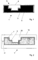
- FIG. 1 shows a chip card 1 according to a first exemplary embodiment, in which a core component 2 from a recyclate and a skin component 3 made of a PC plastic material is.
- the recycled material is shredded and melted plastic material from ABS, for example or PVC and has compared to the skin component an unappealing color.
- the material properties of the Recyclates can be identical to that for skin component 3 used material.
- the core component 2 is completely through the skin component 3 enclosed so that the skin component 3 a protective Layer forms. It preferably takes up 20% of the card volume a, so that the card 1 with any mechanical or temperature-related stress safely through the skin component 3 is protected.
- the bending properties of the card 1 are mainly due to the material of the core component 2 determined.
- the volume fraction of the skin component 3 can but also higher, up to approx. 40%.
- the skin component 3 has a recess 4 in which a Chip module 5 is used and is held in this inseparable.
- the recess 4 can on the one hand after the spraying process Milling generated or on the other hand during the spraying process be formed by lowering a displaceable die.
- a core component 6 made of a thermoplastic elastomer (TPE) and one Skin component 7 made of a high temperature resistant material, for example, PC.
- TPE thermoplastic elastomer
- the chip card 1 will molded in a mold 19, with a molding 20 the recess for later insertion of a chip module.
- An injection point 21 through which the injection material is injected into the mold 19, is about in the middle on a short narrow side of the chip card.
- the card 1 is a core component 8 consisting of an ABS material and a skin component 9 consisting of a Colorant added PC material. This is one any color of card 1 possible.
- FIG. 4 shows a device for injection molding a card, from an injection molding machine 10 with a master cylinder 11 and an auxiliary unit 12 with an auxiliary cylinder 13.
- the cylinders 11, 13 are plasticizing cylinders formed, a skin component in the secondary cylinder 13 14 is plasticized and in a preparatory step the same after moving the auxiliary unit 12 in the nozzle area of the main unit 10 through a main spray nozzle 15
- Injection molding machine 10 is passed into the master cylinder 11.
- the skin component melt displaces in the master cylinder 11 an already melted core component 16.
Landscapes
- Engineering & Computer Science (AREA)
- Computer Hardware Design (AREA)
- Microelectronics & Electronic Packaging (AREA)
- Mechanical Engineering (AREA)
- General Physics & Mathematics (AREA)
- Theoretical Computer Science (AREA)
- Manufacturing & Machinery (AREA)
- Physics & Mathematics (AREA)
- Chemical & Material Sciences (AREA)
- Dispersion Chemistry (AREA)
- Injection Moulding Of Plastics Or The Like (AREA)
- Credit Cards Or The Like (AREA)
- Cosmetics (AREA)
- Electrochromic Elements, Electrophoresis, Or Variable Reflection Or Absorption Elements (AREA)
Claims (14)
- Carte à puce comprenant un corps de carte qui peut être fabriqué par moulage par injection dans l'espace d'un moule en au moins une matière plastique, caractérisée en ce que le corps de carte peut être réalisé d'une part par injection d'une première matière plastique pour former un composant pellicule (3) de la carte à puce (1) et d'autre part par injection d'une deuxième matière plastique pour former un composant âme (2) de la carte à puce (1), le composant pellicule (3) entourant entièrement le composant âme (2) et le composant pellicule (3) présentant une part volumique d'au moins 20% du corps de la carte.
- Carte à puce selon la revendication 1, caractérisée en ce que le composant pellicule (3) présente une part volumique de 20% à 40% du corps de la carte.
- Carte à puce selon la revendication 1 ou 2, caractérisée en ce que le composant pellicule (3) présente un moyen de marquage au laser tel qu'il permet de constituer des informations visibles à l'oeil par le biais d'une transformation locale du matériau du composant pellicule (3) effectuée avec un rayon laser.
- Carte à puce selon l'une des revendications 1 à 3, caractérisée en ce que le moyen de marquage au laser est réalisé sous la forme d'un additif pour laser qui est mélangé à la matière plastique prévue pour le composant pellicule (3).
- Carte à puce selon la revendication 1 ou 2, caractérisée en ce que la première matière plastique associée au composant pellicule (3) est transparente et que la deuxième matière plastique associée au composant âme (2) présente un moyen de marquage au laser.
- Carte à puce selon l'une des revendications 1 à 5, caractérisée en ce que le moyen de marquage au laser est transparent dans la gamme des longueurs d'onde visibles et il est réalisé dans une gamme de longueurs d'onde absorbant le rayon laser.
- Carte à puce selon l'une des revendications 1 à 6, caractérisée en ce que le moyen de marquage au laser présente une coloration sous l'effet du rayon laser.
- Carte à puce selon l'une des revendications 1 à 7, caractérisée en ce que le composant pellicule (3) est réalisé dans une matière plastique pouvant être appliquée par transfert thermique sous pression, plus particulièrement du PVC.
- Carte à puce selon l'une des revendications 1 à 8, caractérisée en ce que le composant pellicule (3) présente une épaisseur comprise entre 0,1 mm et 0,2 mm.
- Carte à puce selon l'une des revendications 1 à 9, caractérisée en ce que le composant âme (2) est constitué de matière recyclée et le composant pellicule (3) de matière plastique de haute qualité.
- Carte à puce selon l'une des revendications 1 à 10, caractérisée en ce que le composant âme (6) est constitué d'un élastomère thermoplastique (TPE) et le composant pellicule (7) d'une matière plastique résistante aux hautes températures.
- Carte à puce selon l'une des revendications 1 à 11, caractérisée en ce que le composant pellicule (9) est constitué d'une matière plastique PC ou d'une matière plastique ABS.
- Carte à puce selon l'une des revendications 1 à 12, caractérisée en ce que, d'une part, le composant âme (8) est constitué d'une matière plastique ABS et, d'autre part, le composant pellicule (9) est constitué d'une matière plastique PC ou d'une matière plastique PMMA ou encore d'un matériau PET.
- Carte à puce selon l'une des revendications 1 à 13, caractérisée en ce que le composant pellicule (9) et/ou le composant âme (8) est constitué d'une matière plastique à laquelle a été ajouté un colorant.
Applications Claiming Priority (2)
| Application Number | Priority Date | Filing Date | Title |
|---|---|---|---|
| DE19736063 | 1997-08-20 | ||
| DE19736063A DE19736063C2 (de) | 1997-08-20 | 1997-08-20 | Chipkarte |
Publications (2)
| Publication Number | Publication Date |
|---|---|
| EP0897784A1 EP0897784A1 (fr) | 1999-02-24 |
| EP0897784B1 true EP0897784B1 (fr) | 2002-05-08 |
Family
ID=7839520
Family Applications (1)
| Application Number | Title | Priority Date | Filing Date |
|---|---|---|---|
| EP98112833A Expired - Lifetime EP0897784B1 (fr) | 1997-08-20 | 1998-07-10 | Carte à puce |
Country Status (5)
| Country | Link |
|---|---|
| US (1) | US20020023962A1 (fr) |
| EP (1) | EP0897784B1 (fr) |
| AT (1) | ATE217247T1 (fr) |
| DE (2) | DE19736063C2 (fr) |
| ES (1) | ES2175563T3 (fr) |
Families Citing this family (9)
| Publication number | Priority date | Publication date | Assignee | Title |
|---|---|---|---|---|
| DE20014560U1 (de) | 2000-08-23 | 2000-10-26 | Smon, Branislav, 71686 Remseck | Flachmaterial, insbesondere zur Herstellung von Kreditkarten, Geldkarten, Telefonkarten o.dgl. |
| DE10207001A1 (de) * | 2002-02-19 | 2003-09-04 | Orga Kartensysteme Gmbh | Chipkarte |
| EP1413978A1 (fr) * | 2002-10-24 | 2004-04-28 | SCHLUMBERGER Systèmes | Support de données |
| DE202004003554U1 (de) * | 2004-03-04 | 2004-06-03 | Novacard Informationssysteme Gmbh | Chipkarte |
| US20090184168A1 (en) * | 2008-01-17 | 2009-07-23 | Roger Ricketts | Recyclable plastic cards and methods of making same |
| US20110084148A1 (en) * | 2009-10-14 | 2011-04-14 | Ricketts Roger H | Plastic cards made from post-consumer plastic |
| CN102233649A (zh) * | 2011-05-06 | 2011-11-09 | 泰德兴精密电子(昆山)有限公司 | 三色产品注塑结构 |
| JP2013022880A (ja) * | 2011-07-22 | 2013-02-04 | Sekisui Techno Seikei Kk | 成形品の製造方法 |
| US9380698B1 (en) * | 2014-12-05 | 2016-06-28 | VivaLnk, Inc. | Stretchable electronic patch having a foldable circuit layer |
Family Cites Families (10)
| Publication number | Priority date | Publication date | Assignee | Title |
|---|---|---|---|---|
| JPS6058819A (ja) * | 1983-09-12 | 1985-04-05 | Kinugawa Rubber Ind Co Ltd | 二層成形品の製法 |
| JPS60176736A (ja) * | 1984-02-23 | 1985-09-10 | Matsushita Electric Works Ltd | 射出成型機 |
| JPS6369613A (ja) * | 1986-09-10 | 1988-03-29 | Mazda Motor Corp | 多層射出成形用の金型構造 |
| DE3711079A1 (de) * | 1987-04-02 | 1988-10-13 | Battenfeld Gmbh | Verfahren und vorrichtung zum spritzgiessen von formteilen aus mindestens zwei verschiedenen kunststoffkomponenten |
| DE3939864A1 (de) * | 1989-12-01 | 1991-06-06 | Gao Ges Automation Org | Mehrschichtige ausweiskarte mit langer lebensdauer |
| DE4142392C2 (de) * | 1991-12-20 | 2003-10-16 | Gao Ges Automation Org | Verfahren und Vorrichtung zum Herstellen von spritzgegossenen Chipkarten mit bereichsweise reduzierter Wandstärke |
| DE4142408A1 (de) * | 1991-12-20 | 1993-06-24 | Gao Ges Automation Org | Ausweiskarte sowie verfahren und vorrichtung zur herstellung derselben |
| US5443378A (en) * | 1994-07-11 | 1995-08-22 | Ferromatik Milacron Maschinenbau Gmbh | Apparatus for the sandwich method of injection molding |
| JP3192341B2 (ja) * | 1994-12-22 | 2001-07-23 | 松下電工株式会社 | 保温食器及びその製造方法 |
| DE19519902C2 (de) * | 1995-05-31 | 1998-03-19 | Richard Herbst | Verfahren zum Herstellen von Gegenständen aus Kunststoff sowie Halbzeug zur Verwendung bei diesem Verfahren |
-
1997
- 1997-08-20 DE DE19736063A patent/DE19736063C2/de not_active Expired - Lifetime
-
1998
- 1998-07-10 DE DE59804029T patent/DE59804029D1/de not_active Expired - Fee Related
- 1998-07-10 EP EP98112833A patent/EP0897784B1/fr not_active Expired - Lifetime
- 1998-07-10 ES ES98112833T patent/ES2175563T3/es not_active Expired - Lifetime
- 1998-07-10 AT AT98112833T patent/ATE217247T1/de not_active IP Right Cessation
- 1998-08-19 US US09/136,451 patent/US20020023962A1/en not_active Abandoned
Also Published As
| Publication number | Publication date |
|---|---|
| DE59804029D1 (de) | 2002-06-13 |
| ATE217247T1 (de) | 2002-05-15 |
| DE19736063C2 (de) | 2000-01-05 |
| US20020023962A1 (en) | 2002-02-28 |
| ES2175563T3 (es) | 2002-11-16 |
| DE19736063A1 (de) | 1999-02-25 |
| EP0897784A1 (fr) | 1999-02-24 |
Similar Documents
| Publication | Publication Date | Title |
|---|---|---|
| EP0888224B1 (fr) | Feuille decorative pour decorer des surfaces de substrat tridimensionnelles | |
| DE69934511T2 (de) | Verfahren und apparat zur herstellung eines verbundprodukts | |
| DE3750765T2 (de) | Mehrschichtige giessdüse. | |
| DE69301656T2 (de) | Dekorationsverfahren für die Oberseite des skis | |
| DE69004031T2 (de) | Verfahren zum Herstellen von Kartenkörpern und Karten mit graphischen Elementen und so erhaltene Karten. | |
| EP0504571A2 (fr) | Moule pour le moulage par injection de corps de brosse à plusieurs composants | |
| DE4237588A1 (fr) | ||
| DE68918245T2 (de) | Verfahren zum Herstellen von Schmuckstücken. | |
| WO2004043669A1 (fr) | Piece moulee par injection | |
| DE102004041833A1 (de) | Dekorierter Spritzgussartikel, Verfahren zur Herstellung eines dekorierten Spritzgussartikels sowie Transferfolie zur Verwendung in einem derartigen Verfahren | |
| EP0897784B1 (fr) | Carte à puce | |
| WO2006066719A2 (fr) | Piece moulee en matiere plastique et procede de realisation | |
| DE102009013789B4 (de) | Polymer-formteil | |
| DE102014011135A1 (de) | Verfahren und Vorrichtung zur Herstellung eines Dekorteils | |
| DE4224171A1 (de) | Spritzgußteil sowie Verfahren und Spritzgießwerkzeug zum Herstellen von Spritzgußteilen | |
| DE1177326B (de) | Verfahren zur Herstellung von aus thermoplastischen Kunststoffen bestehenden kuenstlichen Blumenblaettern und Vorrichtung zur Durchfuehrung dieses Verfahrens | |
| DE68914675T2 (de) | Stabilisiertes spritzgiessen während der anwendung eines gemeinsamen formteils mit separaten komplementären formteilen. | |
| DE3932016C2 (fr) | ||
| DE29717698U1 (de) | Lichtfenster für Signalleuchten, insbesondere für Kraftfahrzeug-Heckleuchten | |
| DE19651714A1 (de) | Dekoriertes Halbzeug aus transparenten Polyamiden Verfahren zu seiner herstellung und dessen Verwendung | |
| DE4339909C2 (de) | Verfahren zur Herstellung eines hintergrundbeleuchteten Spritzgießteils und Spritzgießteil | |
| DE19951785A1 (de) | Verfahren zum Herstellen eines Aussenhautteiles einer Fahrzeugkarosserie | |
| DE4303497A1 (de) | Verfahren zur Herstellung von Mehrkomponenten-Sichtelementen aus Kunststoff | |
| EP3208097A2 (fr) | Objet en plastique imprimé et son procédé et son dispositif de fabrication | |
| DE4442875C1 (de) | Verfahren und Spritzguß-Werkzeug zur Herstellung von Kunststoff-Gliedermaßstäben |
Legal Events
| Date | Code | Title | Description |
|---|---|---|---|
| PUAI | Public reference made under article 153(3) epc to a published international application that has entered the european phase |
Free format text: ORIGINAL CODE: 0009012 |
|
| AK | Designated contracting states |
Kind code of ref document: A1 Designated state(s): AT BE CH DE DK ES FR GB GR IT LI NL PT SE |
|
| AX | Request for extension of the european patent |
Free format text: AL;LT;LV;MK;RO;SI |
|
| 17P | Request for examination filed |
Effective date: 19990312 |
|
| AKX | Designation fees paid |
Free format text: AT BE CH DE DK ES FR GB GR IT LI NL PT SE |
|
| 17Q | First examination report despatched |
Effective date: 19990923 |
|
| RTI1 | Title (correction) |
Free format text: CHIP CARD |
|
| GRAG | Despatch of communication of intention to grant |
Free format text: ORIGINAL CODE: EPIDOS AGRA |
|
| GRAG | Despatch of communication of intention to grant |
Free format text: ORIGINAL CODE: EPIDOS AGRA |
|
| GRAH | Despatch of communication of intention to grant a patent |
Free format text: ORIGINAL CODE: EPIDOS IGRA |
|
| RAP1 | Party data changed (applicant data changed or rights of an application transferred) |
Owner name: ORGA KARTENSYSTEME GMBH |
|
| GRAH | Despatch of communication of intention to grant a patent |
Free format text: ORIGINAL CODE: EPIDOS IGRA |
|
| REG | Reference to a national code |
Ref country code: GB Ref legal event code: IF02 |
|
| GRAA | (expected) grant |
Free format text: ORIGINAL CODE: 0009210 |
|
| AK | Designated contracting states |
Kind code of ref document: B1 Designated state(s): AT BE CH DE DK ES FR GB GR IT LI NL PT SE |
|
| PG25 | Lapsed in a contracting state [announced via postgrant information from national office to epo] |
Ref country code: NL Free format text: LAPSE BECAUSE OF FAILURE TO SUBMIT A TRANSLATION OF THE DESCRIPTION OR TO PAY THE FEE WITHIN THE PRESCRIBED TIME-LIMIT Effective date: 20020508 Ref country code: GR Free format text: LAPSE BECAUSE OF FAILURE TO SUBMIT A TRANSLATION OF THE DESCRIPTION OR TO PAY THE FEE WITHIN THE PRESCRIBED TIME-LIMIT Effective date: 20020508 |
|
| REF | Corresponds to: |
Ref document number: 217247 Country of ref document: AT Date of ref document: 20020515 Kind code of ref document: T |
|
| REG | Reference to a national code |
Ref country code: CH Ref legal event code: EP |
|
| REF | Corresponds to: |
Ref document number: 59804029 Country of ref document: DE Date of ref document: 20020613 |
|
| PG25 | Lapsed in a contracting state [announced via postgrant information from national office to epo] |
Ref country code: BE Free format text: LAPSE BECAUSE OF NON-PAYMENT OF DUE FEES Effective date: 20020731 |
|
| PG25 | Lapsed in a contracting state [announced via postgrant information from national office to epo] |
Ref country code: SE Free format text: LAPSE BECAUSE OF FAILURE TO SUBMIT A TRANSLATION OF THE DESCRIPTION OR TO PAY THE FEE WITHIN THE PRESCRIBED TIME-LIMIT Effective date: 20020808 Ref country code: PT Free format text: LAPSE BECAUSE OF FAILURE TO SUBMIT A TRANSLATION OF THE DESCRIPTION OR TO PAY THE FEE WITHIN THE PRESCRIBED TIME-LIMIT Effective date: 20020808 Ref country code: DK Free format text: LAPSE BECAUSE OF FAILURE TO SUBMIT A TRANSLATION OF THE DESCRIPTION OR TO PAY THE FEE WITHIN THE PRESCRIBED TIME-LIMIT Effective date: 20020808 |
|
| GBT | Gb: translation of ep patent filed (gb section 77(6)(a)/1977) |
Effective date: 20020726 |
|
| ET | Fr: translation filed | ||
| NLV1 | Nl: lapsed or annulled due to failure to fulfill the requirements of art. 29p and 29m of the patents act | ||
| REG | Reference to a national code |
Ref country code: ES Ref legal event code: FG2A Ref document number: 2175563 Country of ref document: ES Kind code of ref document: T3 |
|
| BERE | Be: lapsed |
Owner name: *ORGA KARTENSYSTEME G.M.B.H. Effective date: 20020731 |
|
| PLBE | No opposition filed within time limit |
Free format text: ORIGINAL CODE: 0009261 |
|
| STAA | Information on the status of an ep patent application or granted ep patent |
Free format text: STATUS: NO OPPOSITION FILED WITHIN TIME LIMIT |
|
| 26N | No opposition filed |
Effective date: 20030211 |
|
| PGFP | Annual fee paid to national office [announced via postgrant information from national office to epo] |
Ref country code: GB Payment date: 20060628 Year of fee payment: 9 |
|
| PGFP | Annual fee paid to national office [announced via postgrant information from national office to epo] |
Ref country code: ES Payment date: 20060705 Year of fee payment: 9 |
|
| PGFP | Annual fee paid to national office [announced via postgrant information from national office to epo] |
Ref country code: FR Payment date: 20060720 Year of fee payment: 9 Ref country code: AT Payment date: 20060720 Year of fee payment: 9 |
|
| PGFP | Annual fee paid to national office [announced via postgrant information from national office to epo] |
Ref country code: CH Payment date: 20060724 Year of fee payment: 9 |
|
| PGFP | Annual fee paid to national office [announced via postgrant information from national office to epo] |
Ref country code: DE Payment date: 20060726 Year of fee payment: 9 |
|
| PGFP | Annual fee paid to national office [announced via postgrant information from national office to epo] |
Ref country code: IT Payment date: 20070830 Year of fee payment: 10 |
|
| REG | Reference to a national code |
Ref country code: CH Ref legal event code: PL |
|
| GBPC | Gb: european patent ceased through non-payment of renewal fee |
Effective date: 20070710 |
|
| PG25 | Lapsed in a contracting state [announced via postgrant information from national office to epo] |
Ref country code: LI Free format text: LAPSE BECAUSE OF NON-PAYMENT OF DUE FEES Effective date: 20070731 Ref country code: DE Free format text: LAPSE BECAUSE OF NON-PAYMENT OF DUE FEES Effective date: 20080201 Ref country code: CH Free format text: LAPSE BECAUSE OF NON-PAYMENT OF DUE FEES Effective date: 20070731 |
|
| PG25 | Lapsed in a contracting state [announced via postgrant information from national office to epo] |
Ref country code: GB Free format text: LAPSE BECAUSE OF NON-PAYMENT OF DUE FEES Effective date: 20070710 |
|
| REG | Reference to a national code |
Ref country code: FR Ref legal event code: ST Effective date: 20080331 |
|
| PG25 | Lapsed in a contracting state [announced via postgrant information from national office to epo] |
Ref country code: AT Free format text: LAPSE BECAUSE OF NON-PAYMENT OF DUE FEES Effective date: 20070710 |
|
| PG25 | Lapsed in a contracting state [announced via postgrant information from national office to epo] |
Ref country code: FR Free format text: LAPSE BECAUSE OF NON-PAYMENT OF DUE FEES Effective date: 20070731 |
|
| REG | Reference to a national code |
Ref country code: ES Ref legal event code: FD2A Effective date: 20070711 |
|
| PG25 | Lapsed in a contracting state [announced via postgrant information from national office to epo] |
Ref country code: ES Free format text: LAPSE BECAUSE OF NON-PAYMENT OF DUE FEES Effective date: 20070711 |
|
| PG25 | Lapsed in a contracting state [announced via postgrant information from national office to epo] |
Ref country code: IT Free format text: LAPSE BECAUSE OF NON-PAYMENT OF DUE FEES Effective date: 20080710 |