EP0887940B1 - Nachführungs-Analog-Digital-Wandler - Google Patents
Nachführungs-Analog-Digital-Wandler Download PDFInfo
- Publication number
- EP0887940B1 EP0887940B1 EP98110521A EP98110521A EP0887940B1 EP 0887940 B1 EP0887940 B1 EP 0887940B1 EP 98110521 A EP98110521 A EP 98110521A EP 98110521 A EP98110521 A EP 98110521A EP 0887940 B1 EP0887940 B1 EP 0887940B1
- Authority
- EP
- European Patent Office
- Prior art keywords
- voltage
- analog input
- input voltage
- converter
- analog
- Prior art date
- Legal status (The legal status is an assumption and is not a legal conclusion. Google has not performed a legal analysis and makes no representation as to the accuracy of the status listed.)
- Expired - Lifetime
Links
- 239000003990 capacitor Substances 0.000 claims description 12
- 230000004044 response Effects 0.000 claims description 6
- 230000005641 tunneling Effects 0.000 claims description 4
- 230000008859 change Effects 0.000 claims description 3
- 230000010354 integration Effects 0.000 claims description 3
- 238000005259 measurement Methods 0.000 claims description 2
- 238000006243 chemical reaction Methods 0.000 description 9
- 230000003247 decreasing effect Effects 0.000 description 6
- 238000010586 diagram Methods 0.000 description 5
- 230000007423 decrease Effects 0.000 description 3
- 238000000034 method Methods 0.000 description 3
- 238000013139 quantization Methods 0.000 description 3
- 239000004065 semiconductor Substances 0.000 description 3
- 230000008901 benefit Effects 0.000 description 2
- 230000004888 barrier function Effects 0.000 description 1
- 239000000969 carrier Substances 0.000 description 1
- 230000000295 complement effect Effects 0.000 description 1
- 230000003111 delayed effect Effects 0.000 description 1
- 230000004069 differentiation Effects 0.000 description 1
- 238000007599 discharging Methods 0.000 description 1
- 230000000694 effects Effects 0.000 description 1
- 239000000463 material Substances 0.000 description 1
- 239000002184 metal Substances 0.000 description 1
- 230000008569 process Effects 0.000 description 1
- 230000000630 rising effect Effects 0.000 description 1
- 239000003362 semiconductor superlattice Substances 0.000 description 1
- 230000035945 sensitivity Effects 0.000 description 1
Images


Classifications
-
- H—ELECTRICITY
- H03—ELECTRONIC CIRCUITRY
- H03M—CODING; DECODING; CODE CONVERSION IN GENERAL
- H03M1/00—Analogue/digital conversion; Digital/analogue conversion
- H03M1/12—Analogue/digital converters
- H03M1/50—Analogue/digital converters with intermediate conversion to time interval
Definitions
- This invention relates to electrical analog-to-digital converters, and more particularly to a tracking analog-to-digital converter.
- Analog-to-digital converters are used to translate analog input voltages to digital values which can be used by digital computers. The translation is accomplished by quantizing the analog input voltage and converting the quantization level to a digital code.
- ADCS using an input device producing output current pulses are e.g. disclosed in IBM Technical Disclosure Bulletin, vol. 31, no. 3, pages 257-258, August 1988, or in US 3,160,873 A.
- the ADC of IBM discloses in particular the usage of a superlattice device. An increasing or decreasing input voltage applied to the superlattice device causes a stepped current flowing through the supenattice device. A voltage corresponding to the stepped current is differentiated and produces pulses of different polarity for rising and falling voltages. The pulses can be separated and used as input for an up-down counter which continuously digitises the signal as it changes.
- the parallel ADC architecture commonly referred to as flash converters
- the parallel ADC architecture provides the fastest currently available approach to quantizing an analog signal. Quantization is effectuated by comparing the analog input voltage to successively higher reference voltage levels.
- a bank of comparators is connected to receive an analog input voltage and predetermined reference voltages.
- the reference voltage levels are generated using a resistor spring which divides the total reference voltage into equally spaced voltage levels of decreasing value to provide different quantization levels within the reference voltage range.
- the resolution of a flash converter is determined by the number of comparators used. One n-bit resolution digital signal is produced in each conversion cycle. Each additional bit of resolution causes a doubling of the amount of circuitry that is required.
- the conversion resolution is therefore restricted by the area available for the bank of comparators and string of resistors. Not only do the enormous number of resistors and comparators consume valuable area, it is difficult to produce the low-valued resistors required for flash converters while maintaining the resistor-matching characteristics required for accurate performance. Additional information on parallel ADC architecture can be found in Demler, High-Speed Analog-to-Digital Conversion , Academic Press, San Diego, 1991, at pages 16-18.
- Flash converters have an inherent capacitance characteristic which affects their ability to operate on high frequency analog signals.
- the base-emitter junction of the transistor on the analog input side has an input capacitance with a charging path through the reference ladder. The time required to charge the capacitor causes the reference voltage to lag fast changes in the current which dynamically distorts the voltage division of the reference ladder.
- a track-and-hold (T/H) used with a flash converter overcomes this limitation by holding an analog value so that the comparators are always converting a steady value rather than one which is continuously changing.
- the flash converter is not simultaneously quantizing changes in the analog input voltage.
- the analog input capacitance of comparators and its effect on flash converts is explained in greater detail in Analog Devices, Inc., Analog-Digital Conversion Handbook , P R T Prentic Hall, New Jersey, 1986, pages 423-426.
- Serial ADCs offer higher resolution, but, the total conversion time is greatly increased.
- An example of a serial ADC is the integrating ADC. Integrating ADC's are used in low-speed applications where high accuracy is of primary importance, and are described in Demler, High-Speed Analog-to-Digital Conversion , supra, pages 2-4.
- the digital output is directly proportional to the voltage level of the analog input voltage.
- the speed of the integrating ADC is limited by the number of bits of the digital output code. Increasing the resolution by one bit requires double the number of clock cycles. Because of the speed limitations, the integrating ADC is not suitable for converting fast changing analog input voltages.
- the tracking converter of the present invention as defined in claim 1 incorporates an input device which produces a pulsating current corresponding to the ADC's analog input voltage.
- the pulsating output is encoded to provide a unique digital code which can be read to yield an approximation of the analog input voltage level.
- An advantace of the tracking converter of this invention is that it operates at higher frequency rates.
- the tracking ADC overcomes the accuracy limitation of flash converters and the speed limitations of serial ADCs. As a result, it is capable of converting high frequency analog input voltages more accurately.
- the input device is a superlattice having a plurality of resonances.
- the number of resonances in the superlattice determines the resolution of the tracking converter.
- Superlattices can be vertically stacked to increase the resolution of the tracking converter without taking up valuable "chip real estate".
- a plurality of resonant-tunneling diodes produce the pulsating current. Increasing the number of resonant-tunneling diodes increases the resolution of the tracking ADC.
- FIG. 1 illustrates the current-voltage (I-V) characteristic 2 of an input device.
- I-V current-voltage
- the invention is described using a superlattice as the input device although other devices, such as resonant-tunneling diodes, may be substituted.
- superlattices have a plurality of resonances, referred to as minibands.
- Each miniband of a superlattice is similar to that of a metal-insulator-metal barrier of a tunnel diode or capacitor.
- When a voltage is applied carriers can tunnel from the first miniband to the second miniband until the input voltage exceeds the width of the first miniband.
- Semiconductor superlattices have been incorporated in high speed tunnel diodes, referred to as superlattice tunnel diodes. This type of diode is described in Sze, High Speed Semiconductor Devices , John Wiley & Sons, Inc., New York, 1990, pages 528-530.
- each miniband 10 along the voltage axis 12 has a bandwidth with a lower and upper threshold voltage, 14 and 16 , respectively.
- a lower threshold voltage 14 and 16 , respectively.
- the voltage level applied to the device exceeds the lower threshold 14 of a miniband 10 , that miniband 10 conducts until the upper threshold 16 is exceeded.
- FIG. 2a illustrates the relationship between an analog input voltage 18 and the I-V characteristic 2 of the superlattice .
- the horizontal voltage axis 12 is common for both while the two vertical axis are different.
- the superlattice current is graphed with respect to voltage while the analog input voltage is graphed with respect to time.
- the two graphs are illustrated together to simplify the explanation of the operation of the invention.
- the functionality of the invention is described with operation in the first quadrant of the superlattice I-V characteristic 2 plane.
- the superlattice operates in a converse manner following the I-V characteristics 2 in the third quadrant as shown in FIG. 1.
- FIG. 2a is a graph of the pulsating output current 24 , with respect to time, which is generated when the analog input voltage 18 is applied to the superlattice.
- analog input voltage 18 exceeds the first minibands 20 lower threshold 14 during most of the first time period 26 and exceeds the second minibands 22 lower threshold 14 during the second time period.
- the slope of the pulsating output current 24 pulse is dependant on the change in analog input voltage 18 with respect to time. As shown in FIG. 2b, the slope of the current pulse increases during the time period between the lower threshold 14 and the upper threshold 16 being exceeded as shown in pulses 32 and 34 . At the point where the analog input voltage 18 exceeds the upper threshold 16 , the current pulses 32 and 34 in FIG. 2b are shown decreasing.
- the analog input voltage 18 is a decreasing positive value.
- the resulting current output pulse 36 shown in FIG. 2b, increases sharply until the upper threshold 16 is no longer exceeded and decreases until the lower threshold 14 is no longer exceeded.
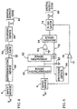
- the input device 4 a suneriaccice in this example, is connected to encoding device 38 which produces a digital output code 40 corresponding to the voltage level of the analog input voltage 18 applied.
- the encoding logic 38 may take many forms.
- differentiating device 42 differentiates the pulsating output current 24 to control the count of counting device 44 .
- Differentiation of the pulsating output current 24 results in the differentiated voltage 46 shown in FIG. 2c, having alternating positive and negative portions 48 and 50 , respectively.
- FIGs. 2b-2d are illustrated together to show the relationship between the waveforms.
- the differentiated voltage 46 is positive when the pulsating current 24 amplitude is increasing, and negative when it is decreasing.
- the sum of the area of the positive portion 48 and negative portion 50 , for the first period is positive since the voltage level of the analog input voltage 18 exceeds the upper threshold 16 of the first miniband 20 .
- the analog input voltage 18 does not exceed the upper threshold 16 of the third miniband 52 , resulting in a total area for that period equal to zero.
- the total area of the differentiated voltage 46 for the corresponding period is negative.
- Logic gate 54 shown in FIG. 4, following the differentiating device 42 can be used to provide a logic signal to control the direction counting device 44 counts.
- the counter may count up when the differentiated voltage 46 is positive, shown by area 48 in FIG. 2b, and count down when it is negative.
- the resulting digital output code 40 provides a unique digital value corresponding to an approximate measurement of analog input voltage 18.
- the digital output code 40 tracks changes in the voltage level of analog input voltage 18 .
- the tracking ADC provides a continuous approximation of the analog input voltage 18 .
- an integrating device 60 sums the area of each period of differentiated voltage 46.
- Integrating device 60 in this example includes an integrating capacitor 62 and a switching device 64 for discharging the integrating capacitor 62 .
- FIG. 2d is a graph of the integrated voltage 66 resulting from integration of differentiated voltage 46. As shown by the voltage ramp 68 in FIG. 2d, the charge on the integrating capacitor 62 increases to a level which is directly proportional to the voltage level of the positive portion 48 of the differentiated voltage 46. During the negative portion 50 of the period, the charge on the integrating capacitor 62 decreases as shown by the decreasing voltage ramp 70 .
- the polarity of the charge on the capacitor indicates a positive or negative area for that period.
- the charge on integrating capacitor 62 is positive.
- the charge is zero at the end of the third period and negative following summation of the forth period.
- a switching device 64 which monitors differentiated voltage 46 will provide a discharge path for integrating capacitor 62 following each period.
- a logic gate 54 following integrating device 60 may be used to control the direction which counting device 44 counts.
- Counting device 44 will count up or down one count following each period of differentiated voltage 46 .
- a trigger 72 derived from a delayed differentiated voltage 46 can be used to trigger the counting device 44 at the end of each period.
- counting device 44 may be connected to count up when the charge on the integrating capacitor 62 is positive and down when the charge is negative.
- Comparator 76 compares the analog input voltage 18 to a known reference voltage, a ground reference in this example, to produce a digital one when the analog input voltage 18 is positive, and a zero when negative. The output of comparator 76 instructs the latch 74 to display a true count when the analog input voltage 18 is positive and the two's complement of the count when the analog input voltage 18 is negative to provide a discrete digital output code 40 corresponding to the voltage level of analog input voltage 18 .
- Every trigger pulse 72 counting device 44 produces a digital output code 40 which corresponds to the voltage level of the analog input voltage 18 .
- Tracking changes in the analog input voltage 18 allows the new ADC described in this invention co overcome the speed limitations of known parallel and serial converters.
- Composing superlattice to have an increased number of resonances improves the resolution of the tracking ADC.
- Another method of increasing the resolution is level shifting. By shifting the voltage response threshold of successive superlattices to respond to correspondingly higher analog input voltage levels, higher resolution is accomplished. Additional information on the composition and performance of superlattice semiconductors can be found in Fink and Christian, Semiconductor Materials, Electronics Engineers' Handbook , Third Edition, McGraw-Hill Book Company, New York, 1989, pages 6-82 through 6-90.
- the first superlattice may be composed to respond to voltage levels from zero to two volts.
- the threshold of the second superlattice may be shifted to respond to voltage levels between two and four volts.
- a third superlattice may be shifted to respond to voltages between four and six volts.
- tracking ADC was described with a superlattice input device, other devices, such as a plurality of resonance tunneling diodes, could be used to emulate the superlattice structure.
- devices such as a plurality of resonance tunneling diodes, could be used to emulate the superlattice structure.
- embodiments were illustrated using a differentiating device, integrating device, and counting devices, alternative encoding devices could be used.
- the present invention discloses a tracking analog-to-digital converter (ADC) which incorporates an input device 4, such as a superlattice, which produces a pulsating output current 24 corresponding to the voltage level of an analog input voltage 18, and an encoding device 38 to provide a unique digital code 40 which can be read to yield an approximation of the voltage level of the analog input voltage 18.
- ADC tracking analog-to-digital converter
- the device operates at higher speeds than previously attainable.
- the resolution of the new ADC is increased by composing the input device 4 to respond to narrow voltage ranges.
- narrow response ranges are accomplished by composing the superlattice to have an increased number of minibands 10 or by vertically stacking a plurality of superlattices.
Landscapes
- Engineering & Computer Science (AREA)
- Theoretical Computer Science (AREA)
- Analogue/Digital Conversion (AREA)
Claims (5)
- Nachführungs-Analog-Digital-Wandler zum Wandeln einer analogen Eingangsspannung (18) in einen digitalen Ausgangs-Code (40) mit:einer Eingangsvorrichtung (4) mit einer Strom-Spannungs-Charakteristik (2), die die Eingangsvorrichtung Ausgangs-Stromimpulse (24) in Antwort auf die analoge Eingangsspannung erzeugen lässt, wobei die Steigung der pulsierenden Ausgangs-Stromimpulse (24) abhängig von der Änderung der analogen Eingangsspannung bezüglich der Zeit ist, und wobei jeder Impuls eine Zeitlänge besitzt, die eine Periode definiert,einer Codiervorrichtung (38), die angeordnet ist, um auf die Ausgangs-Stromimpulse anzusprechen, indem der digitale Ausgangscode entsprechend einer ungefähren Messung der analogen Eingangsspannung erzeugt wird und die eine Differenzierungsvorrichtung (42) aufweist, die mit der Eingangsvorrichtung (4) verbunden ist, die die Ausgangs-Stromimpulse differenziert, um eine differenzierte Spannung (46) mit abwechselnder Polarität zu erzeugen, dadurch gekennzeichnet, dass die Codiervorrichtung (38) ferner aufweisteine Integrations-Vorrichtung (60), um die differenzierte Spannung für jede Periode zu summieren und eine integrierte Spannung (66) entgegengesetzter Polarität für positive und negative Summierungen zu erzeugen, wobei die Integrations-Vorrichtung (60) aufweist:einen Integrations-Kondensator (62), der angeordnet ist, um auf einen Spannungspegel etwa gleich einem Spannungspegel direkt proportional zu der Integration der differenzierten Spannung über die Periode aufgeladen wird, undeine Schalt-Vorrichtung (64), um einen Entladepfad für den Integrations-Kondensator (62) auf jede Periode folgend bereitzustellen,ein Logikgatter (54), um die integrierte Spannung in ein entsprechendes Logiksignal umzuwandeln, undeine Zählvorrichtung (44), die angeordnet ist, um das Logiksignal zu empfangen, um den digitalen Ausgangscode (40) zu erzeugen.
- Wandler nach Anspruch 1, dadurch gekennzeichnet, dass die Eingangsvorrichtung (4) eine Vielzahl von Resonanztunneldioden aufweist, deren jede auf einen jeweils zunehmenden höheren Pegel der analogen Eingangsspannung (18) anspricht, wobei die Vielzahl von Resonanztunneldioden die Ausgangs-Stromimpulse erzeugen entsprechend der Anzahl der Vielzahl von Resonanztunneldioden, die leiten.
- Wandler nach Anspruch 1, dadurch gekennzeichnet, dass die Eingangsvorrichtung (4) ein Superlattice ist mit einer Vielzahl von Minibändern (10), die abhängig von der analogen Eingangsspannung (18) leiten, die die jeweiligen Schwellenwertpegel für die Vielzahl von Minibändern überschreitet, wobei das Superlattice die Ausgangs-Stromimpulse entsprechend der Anzahl der Vielzahl von Minibändern (10), die leiten, erzeugt.
- Wandler nach Anspruch 1 oder 3, dadurch gekennzeichnet, dass die Eingangsvorrichtung (4) eine Vielzahl von Superlattice umfasst, die vertikal gestapelt sind, um den Eingangsspannungsbetriebsbereich des Wandlers zu erhöhen, wobei die Vielzahl von Superlattice jeweils einen Spannungs-Ansprechschwellenwert besitzt.
- Wandler nach Anspruch 4, dadurch gekennzeichnet, dass der Spannungs-Ansprechschwellenwert von aufeinander folgenden Superlattice der Vielzahl von Superlattice verschoben wird, um auf entsprechend höhere Spannungspegel der analogen Eingangsspannung anzusprechen, um den Eingangsspannungsbetriebsbereich zu erhöhen.
Applications Claiming Priority (2)
| Application Number | Priority Date | Filing Date | Title |
|---|---|---|---|
| US08/880,283 US5945934A (en) | 1997-06-23 | 1997-06-23 | Tracking analog-to-digital converter |
| US880283 | 1997-06-23 |
Publications (3)
| Publication Number | Publication Date |
|---|---|
| EP0887940A2 EP0887940A2 (de) | 1998-12-30 |
| EP0887940A3 EP0887940A3 (de) | 2002-10-09 |
| EP0887940B1 true EP0887940B1 (de) | 2005-04-27 |
Family
ID=25375952
Family Applications (1)
| Application Number | Title | Priority Date | Filing Date |
|---|---|---|---|
| EP98110521A Expired - Lifetime EP0887940B1 (de) | 1997-06-23 | 1998-06-09 | Nachführungs-Analog-Digital-Wandler |
Country Status (4)
| Country | Link |
|---|---|
| US (1) | US5945934A (de) |
| EP (1) | EP0887940B1 (de) |
| JP (1) | JP3977516B2 (de) |
| DE (1) | DE69829915T2 (de) |
Families Citing this family (3)
| Publication number | Priority date | Publication date | Assignee | Title |
|---|---|---|---|---|
| GB9827932D0 (en) * | 1998-12-19 | 1999-02-10 | Secr Defence | Analogue to digital converter and method of analogue to digital conversion |
| ITMI20011996A1 (it) * | 2001-09-26 | 2003-03-26 | St Microelectronics Srl | Convertitore analogico digitale ad inseguimento |
| US7586427B1 (en) * | 2008-04-24 | 2009-09-08 | Northrop Grumman Corporation | Sequential triggering of series-connected resonant tunneling diodes |
Family Cites Families (2)
| Publication number | Priority date | Publication date | Assignee | Title |
|---|---|---|---|---|
| US3160873A (en) * | 1960-10-24 | 1964-12-08 | Rca Corp | Negative resistance analog to digital converter |
| US3937066A (en) * | 1973-11-01 | 1976-02-10 | Stanford Research Institute | Ultrasonic camera system and method |
-
1997
- 1997-06-23 US US08/880,283 patent/US5945934A/en not_active Expired - Lifetime
-
1998
- 1998-06-09 DE DE69829915T patent/DE69829915T2/de not_active Expired - Lifetime
- 1998-06-09 EP EP98110521A patent/EP0887940B1/de not_active Expired - Lifetime
- 1998-06-23 JP JP17619598A patent/JP3977516B2/ja not_active Expired - Lifetime
Also Published As
| Publication number | Publication date |
|---|---|
| JP3977516B2 (ja) | 2007-09-19 |
| US5945934A (en) | 1999-08-31 |
| JPH1188168A (ja) | 1999-03-30 |
| DE69829915T2 (de) | 2006-03-09 |
| DE69829915D1 (de) | 2005-06-02 |
| EP0887940A2 (de) | 1998-12-30 |
| EP0887940A3 (de) | 2002-10-09 |
Similar Documents
| Publication | Publication Date | Title |
|---|---|---|
| US6002356A (en) | Power saving flash A/D converter | |
| US6747589B2 (en) | Error correction architecture to increase speed and relax current drive requirements of SAR ADC | |
| US4672359A (en) | Superconducting analog-to-digital converter and digital magnetometer and related method for its use | |
| Draxelmayr | A 6b 600MHz 10mW ADC array in digital 90nm CMOS | |
| EP0227165B1 (de) | Schaltung zur Interpolation zwischen komplementären Spannungen | |
| US4978957A (en) | High-speed analog-to-digital converter | |
| WO2010055492A2 (en) | Time interpolation flash adc having automatic feedback calibration | |
| EP2238689A1 (de) | Analog-digital-wandler mit komparatorbasierter asynchroner binärer suche | |
| Wei et al. | A self-latching A/D converter using resonant tunneling diodes | |
| EP0609916B1 (de) | Supraleitender Analog-Digitalwandler und Leseverfahren dafür | |
| EP0887940B1 (de) | Nachführungs-Analog-Digital-Wandler | |
| EP0070734A2 (de) | Analog-Digital-Wandler | |
| US3859654A (en) | Analog to digital converter for electrical signals | |
| CN1522496A (zh) | 处理磁泡的模拟变量位转换器校准 | |
| US6677877B2 (en) | Comparator, analog-to-digital converter and method of analog-to-digital conversion using non-linear magneto-electronic device | |
| US6710735B1 (en) | Dual supply voltage pipelined ADC | |
| US5012243A (en) | Superconducting analog-to-digital converter with floating four-junction squid bidirectional counter | |
| US4591830A (en) | Comparator cell for analog-to-digital flash converter | |
| US20040257257A1 (en) | A/D converter and A/D conversion method | |
| US4654587A (en) | Digital peak detector and method of peak detection | |
| US11522555B1 (en) | Multistage analog-to-digital converters for crossbar-based circuits | |
| EP0259936B1 (de) | Kodeumsetzer mit komplementären Ausgangsspannungen | |
| CN110380728A (zh) | 一种高分辨率的混合模数电路转换装置及转换方法 | |
| KR20000070087A (ko) | 반도체 집적 회로, 동작 상태 검출기 및 전자 기기 | |
| US20030160716A1 (en) | Shared parallel digital-to-analog conversion |
Legal Events
| Date | Code | Title | Description |
|---|---|---|---|
| PUAI | Public reference made under article 153(3) epc to a published international application that has entered the european phase |
Free format text: ORIGINAL CODE: 0009012 |
|
| AK | Designated contracting states |
Kind code of ref document: A2 Designated state(s): AT BE CH CY DE DK ES FI FR GB GR IE IT LI LU MC NL PT SE |
|
| AX | Request for extension of the european patent |
Free format text: AL;LT;LV;MK;RO;SI |
|
| PUAL | Search report despatched |
Free format text: ORIGINAL CODE: 0009013 |
|
| RIC1 | Information provided on ipc code assigned before grant |
Free format text: 7H 03M 1/48 A, 7H 03M 1/50 B |
|
| AK | Designated contracting states |
Kind code of ref document: A3 Designated state(s): AT BE CH CY DE DK ES FI FR GB GR IE IT LI LU MC NL PT SE |
|
| AX | Request for extension of the european patent |
Free format text: AL;LT;LV;MK;RO;SI |
|
| 17P | Request for examination filed |
Effective date: 20030314 |
|
| AKX | Designation fees paid |
Designated state(s): DE FR GB |
|
| 17Q | First examination report despatched |
Effective date: 20030718 |
|
| GRAP | Despatch of communication of intention to grant a patent |
Free format text: ORIGINAL CODE: EPIDOSNIGR1 |
|
| GRAS | Grant fee paid |
Free format text: ORIGINAL CODE: EPIDOSNIGR3 |
|
| GRAA | (expected) grant |
Free format text: ORIGINAL CODE: 0009210 |
|
| AK | Designated contracting states |
Kind code of ref document: B1 Designated state(s): DE FR GB |
|
| REG | Reference to a national code |
Ref country code: GB Ref legal event code: FG4D |
|
| REG | Reference to a national code |
Ref country code: IE Ref legal event code: FG4D |
|
| REF | Corresponds to: |
Ref document number: 69829915 Country of ref document: DE Date of ref document: 20050602 Kind code of ref document: P |
|
| PLBE | No opposition filed within time limit |
Free format text: ORIGINAL CODE: 0009261 |
|
| STAA | Information on the status of an ep patent application or granted ep patent |
Free format text: STATUS: NO OPPOSITION FILED WITHIN TIME LIMIT |
|
| ET | Fr: translation filed | ||
| 26N | No opposition filed |
Effective date: 20060130 |
|
| REG | Reference to a national code |
Ref country code: FR Ref legal event code: PLFP Year of fee payment: 19 |
|
| REG | Reference to a national code |
Ref country code: FR Ref legal event code: PLFP Year of fee payment: 20 |
|
| PGFP | Annual fee paid to national office [announced via postgrant information from national office to epo] |
Ref country code: FR Payment date: 20170627 Year of fee payment: 20 Ref country code: GB Payment date: 20170627 Year of fee payment: 20 |
|
| PGFP | Annual fee paid to national office [announced via postgrant information from national office to epo] |
Ref country code: DE Payment date: 20170628 Year of fee payment: 20 |
|
| REG | Reference to a national code |
Ref country code: DE Ref legal event code: R071 Ref document number: 69829915 Country of ref document: DE |
|
| REG | Reference to a national code |
Ref country code: GB Ref legal event code: PE20 Expiry date: 20180608 |
|
| PG25 | Lapsed in a contracting state [announced via postgrant information from national office to epo] |
Ref country code: GB Free format text: LAPSE BECAUSE OF EXPIRATION OF PROTECTION Effective date: 20180608 |