EP0886810B1 - Multi-tool positioning system - Google Patents
Multi-tool positioning system Download PDFInfo
- Publication number
- EP0886810B1 EP0886810B1 EP97908012A EP97908012A EP0886810B1 EP 0886810 B1 EP0886810 B1 EP 0886810B1 EP 97908012 A EP97908012 A EP 97908012A EP 97908012 A EP97908012 A EP 97908012A EP 0886810 B1 EP0886810 B1 EP 0886810B1
- Authority
- EP
- European Patent Office
- Prior art keywords
- fast
- movable
- stage
- slow
- positioner
- Prior art date
- Legal status (The legal status is an assumption and is not a legal conclusion. Google has not performed a legal analysis and makes no representation as to the accuracy of the status listed.)
- Expired - Lifetime
Links
Images


Classifications
-
- B—PERFORMING OPERATIONS; TRANSPORTING
- B23—MACHINE TOOLS; METAL-WORKING NOT OTHERWISE PROVIDED FOR
- B23K—SOLDERING OR UNSOLDERING; WELDING; CLADDING OR PLATING BY SOLDERING OR WELDING; CUTTING BY APPLYING HEAT LOCALLY, e.g. FLAME CUTTING; WORKING BY LASER BEAM
- B23K26/00—Working by laser beam, e.g. welding, cutting or boring
- B23K26/08—Devices involving relative movement between laser beam and workpiece
-
- B—PERFORMING OPERATIONS; TRANSPORTING
- B23—MACHINE TOOLS; METAL-WORKING NOT OTHERWISE PROVIDED FOR
- B23K—SOLDERING OR UNSOLDERING; WELDING; CLADDING OR PLATING BY SOLDERING OR WELDING; CUTTING BY APPLYING HEAT LOCALLY, e.g. FLAME CUTTING; WORKING BY LASER BEAM
- B23K26/00—Working by laser beam, e.g. welding, cutting or boring
- B23K26/08—Devices involving relative movement between laser beam and workpiece
- B23K26/082—Scanning systems, i.e. devices involving movement of the laser beam relative to the laser head
-
- B—PERFORMING OPERATIONS; TRANSPORTING
- B23—MACHINE TOOLS; METAL-WORKING NOT OTHERWISE PROVIDED FOR
- B23K—SOLDERING OR UNSOLDERING; WELDING; CLADDING OR PLATING BY SOLDERING OR WELDING; CUTTING BY APPLYING HEAT LOCALLY, e.g. FLAME CUTTING; WORKING BY LASER BEAM
- B23K26/00—Working by laser beam, e.g. welding, cutting or boring
- B23K26/08—Devices involving relative movement between laser beam and workpiece
- B23K26/083—Devices involving movement of the workpiece in at least one axial direction
-
- B—PERFORMING OPERATIONS; TRANSPORTING
- B23—MACHINE TOOLS; METAL-WORKING NOT OTHERWISE PROVIDED FOR
- B23K—SOLDERING OR UNSOLDERING; WELDING; CLADDING OR PLATING BY SOLDERING OR WELDING; CUTTING BY APPLYING HEAT LOCALLY, e.g. FLAME CUTTING; WORKING BY LASER BEAM
- B23K26/00—Working by laser beam, e.g. welding, cutting or boring
- B23K26/08—Devices involving relative movement between laser beam and workpiece
- B23K26/083—Devices involving movement of the workpiece in at least one axial direction
- B23K26/0853—Devices involving movement of the workpiece in at least two axial directions, e.g. in a plane
-
- G—PHYSICS
- G05—CONTROLLING; REGULATING
- G05B—CONTROL OR REGULATING SYSTEMS IN GENERAL; FUNCTIONAL ELEMENTS OF SUCH SYSTEMS; MONITORING OR TESTING ARRANGEMENTS FOR SUCH SYSTEMS OR ELEMENTS
- G05B19/00—Program-control systems
- G05B19/02—Program-control systems electric
- G05B19/18—Numerical control [NC], i.e. automatically operating machines, in particular machine tools, e.g. in a manufacturing environment, so as to execute positioning, movement or co-ordinated operations by means of program data in numerical form
- G05B19/19—Numerical control [NC], i.e. automatically operating machines, in particular machine tools, e.g. in a manufacturing environment, so as to execute positioning, movement or co-ordinated operations by means of program data in numerical form characterised by positioning or contouring control systems, e.g. to control position from one programmed point to another or to control movement along a programmed continuous path
- G05B19/39—Numerical control [NC], i.e. automatically operating machines, in particular machine tools, e.g. in a manufacturing environment, so as to execute positioning, movement or co-ordinated operations by means of program data in numerical form characterised by positioning or contouring control systems, e.g. to control position from one programmed point to another or to control movement along a programmed continuous path using a combination of the means covered by at least two of the preceding groups G05B19/21, G05B19/27 and G05B19/33
-
- H—ELECTRICITY
- H05—ELECTRIC TECHNIQUES NOT OTHERWISE PROVIDED FOR
- H05K—PRINTED CIRCUITS; CASINGS OR CONSTRUCTIONAL DETAILS OF ELECTRIC APPARATUS; MANUFACTURE OF ASSEMBLAGES OF ELECTRICAL COMPONENTS
- H05K3/00—Apparatus or processes for manufacturing printed circuits
- H05K3/0011—Working of insulating substrates or insulating layers
- H05K3/0017—Etching of the substrate by chemical or physical means
- H05K3/0026—Etching of the substrate by chemical or physical means by laser ablation
- H05K3/0032—Etching of the substrate by chemical or physical means by laser ablation of organic insulating material
- H05K3/0038—Etching of the substrate by chemical or physical means by laser ablation of organic insulating material combined with laser drilling through a metal layer
-
- G—PHYSICS
- G05—CONTROLLING; REGULATING
- G05B—CONTROL OR REGULATING SYSTEMS IN GENERAL; FUNCTIONAL ELEMENTS OF SUCH SYSTEMS; MONITORING OR TESTING ARRANGEMENTS FOR SUCH SYSTEMS OR ELEMENTS
- G05B2219/00—Program-control systems
- G05B2219/30—Nc systems
- G05B2219/34—Director, elements to supervisory
- G05B2219/34047—Dsp digital signal processor
-
- G—PHYSICS
- G05—CONTROLLING; REGULATING
- G05B—CONTROL OR REGULATING SYSTEMS IN GENERAL; FUNCTIONAL ELEMENTS OF SUCH SYSTEMS; MONITORING OR TESTING ARRANGEMENTS FOR SUCH SYSTEMS OR ELEMENTS
- G05B2219/00—Program-control systems
- G05B2219/30—Nc systems
- G05B2219/34—Director, elements to supervisory
- G05B2219/34391—Synchronize axis movement and tool action, delay action, simulation inertia
-
- G—PHYSICS
- G05—CONTROLLING; REGULATING
- G05B—CONTROL OR REGULATING SYSTEMS IN GENERAL; FUNCTIONAL ELEMENTS OF SUCH SYSTEMS; MONITORING OR TESTING ARRANGEMENTS FOR SUCH SYSTEMS OR ELEMENTS
- G05B2219/00—Program-control systems
- G05B2219/30—Nc systems
- G05B2219/36—Nc in input of data, input key till input tape
- G05B2219/36029—Basic
-
- G—PHYSICS
- G05—CONTROLLING; REGULATING
- G05B—CONTROL OR REGULATING SYSTEMS IN GENERAL; FUNCTIONAL ELEMENTS OF SUCH SYSTEMS; MONITORING OR TESTING ARRANGEMENTS FOR SUCH SYSTEMS OR ELEMENTS
- G05B2219/00—Program-control systems
- G05B2219/30—Nc systems
- G05B2219/41—Servomotor, servo controller till figures
- G05B2219/41331—Galvano driver
-
- G—PHYSICS
- G05—CONTROLLING; REGULATING
- G05B—CONTROL OR REGULATING SYSTEMS IN GENERAL; FUNCTIONAL ELEMENTS OF SUCH SYSTEMS; MONITORING OR TESTING ARRANGEMENTS FOR SUCH SYSTEMS OR ELEMENTS
- G05B2219/00—Program-control systems
- G05B2219/30—Nc systems
- G05B2219/42—Servomotor, servo controller kind till VSS
- G05B2219/42209—Two slides, fine and quick, coarse and slow, piggyback, multirate positioner
-
- G—PHYSICS
- G05—CONTROLLING; REGULATING
- G05B—CONTROL OR REGULATING SYSTEMS IN GENERAL; FUNCTIONAL ELEMENTS OF SUCH SYSTEMS; MONITORING OR TESTING ARRANGEMENTS FOR SUCH SYSTEMS OR ELEMENTS
- G05B2219/00—Program-control systems
- G05B2219/30—Nc systems
- G05B2219/42—Servomotor, servo controller kind till VSS
- G05B2219/42219—Slow positioning with low pass, concurrent quick with high pass part of command
-
- G—PHYSICS
- G05—CONTROLLING; REGULATING
- G05B—CONTROL OR REGULATING SYSTEMS IN GENERAL; FUNCTIONAL ELEMENTS OF SUCH SYSTEMS; MONITORING OR TESTING ARRANGEMENTS FOR SUCH SYSTEMS OR ELEMENTS
- G05B2219/00—Program-control systems
- G05B2219/30—Nc systems
- G05B2219/45—Nc applications
- G05B2219/45041—Laser cutting
-
- G—PHYSICS
- G05—CONTROLLING; REGULATING
- G05B—CONTROL OR REGULATING SYSTEMS IN GENERAL; FUNCTIONAL ELEMENTS OF SUCH SYSTEMS; MONITORING OR TESTING ARRANGEMENTS FOR SUCH SYSTEMS OR ELEMENTS
- G05B2219/00—Program-control systems
- G05B2219/30—Nc systems
- G05B2219/45—Nc applications
- G05B2219/45139—Laser drilling
-
- H—ELECTRICITY
- H05—ELECTRIC TECHNIQUES NOT OTHERWISE PROVIDED FOR
- H05K—PRINTED CIRCUITS; CASINGS OR CONSTRUCTIONAL DETAILS OF ELECTRIC APPARATUS; MANUFACTURE OF ASSEMBLAGES OF ELECTRICAL COMPONENTS
- H05K2203/00—Indexing scheme relating to apparatus or processes for manufacturing printed circuits covered by H05K3/00
- H05K2203/01—Tools for processing; Objects used during processing
- H05K2203/0147—Carriers and holders
- H05K2203/0165—Holder for holding a Printed Circuit Board [PCB] during processing, e.g. during screen printing
-
- H—ELECTRICITY
- H05—ELECTRIC TECHNIQUES NOT OTHERWISE PROVIDED FOR
- H05K—PRINTED CIRCUITS; CASINGS OR CONSTRUCTIONAL DETAILS OF ELECTRIC APPARATUS; MANUFACTURE OF ASSEMBLAGES OF ELECTRICAL COMPONENTS
- H05K2203/00—Indexing scheme relating to apparatus or processes for manufacturing printed circuits covered by H05K3/00
- H05K2203/10—Using electric, magnetic and electromagnetic fields; Using laser light
- H05K2203/107—Using laser light
- H05K2203/108—Using a plurality of lasers or laser light with a plurality of wavelengths
-
- H—ELECTRICITY
- H05—ELECTRIC TECHNIQUES NOT OTHERWISE PROVIDED FOR
- H05K—PRINTED CIRCUITS; CASINGS OR CONSTRUCTIONAL DETAILS OF ELECTRIC APPARATUS; MANUFACTURE OF ASSEMBLAGES OF ELECTRICAL COMPONENTS
- H05K3/00—Apparatus or processes for manufacturing printed circuits
- H05K3/0008—Apparatus or processes for manufacturing printed circuits for aligning or positioning of tools relative to the circuit board
-
- H—ELECTRICITY
- H05—ELECTRIC TECHNIQUES NOT OTHERWISE PROVIDED FOR
- H05K—PRINTED CIRCUITS; CASINGS OR CONSTRUCTIONAL DETAILS OF ELECTRIC APPARATUS; MANUFACTURE OF ASSEMBLAGES OF ELECTRICAL COMPONENTS
- H05K3/00—Apparatus or processes for manufacturing printed circuits
- H05K3/0011—Working of insulating substrates or insulating layers
- H05K3/0017—Etching of the substrate by chemical or physical means
Definitions
- This invention relates to an apparatus and a method for positioning multiple "tools,” such as laser beams or other radiation beams, relative to target locations on multiple associated workpieces and, in particular, to a system that accurately coordinates the positioning of the multiple tools and associated target locations with a multi-stage, multi-head positioner.
- tools such as laser beams or other radiation beams
- micro-dimensioned drills may be used to form a cradle for a micro-dimensioned motor; a micro-dimensioned punch may be used to punch holes in a thin metal plate; a laser may be used to precisely machine or selectively erode metallic, crystalline, or amorphous specimens; and ion beams may be used to selectively implant charged particles into an integrated circuit. All of the above-mentioned processes share a common requirement for accurately and rapidly positioning a pertinent tool to target locations on the workpiece.
- multiple tools are simultaneously positioned relative to multiple corresponding workpieces to improve the processing throughput and reduce total manufacturing cost.
- One such application employs a multiple spindle drilling machine to simultaneously drill identical sets of holes in multiple circuit boards.
- Such machines have high throughput but require accurate fixturing of the multiple workpieces, cannot compensate for dimensional differences among the workpieces, and are subject to frequent downtime for drill replacement.
- prior workers have employed lasers to machine via holes between the upper layers of a multilayer circuit board. Such machines have high accuracy and do not require drill replacement, but they do not have the high throughput of multiple spindle drilling machines.
- Existing positioners are typically characterized by low speed and long movement or high speed and short movement.
- Low-speed and long-movement positioners such as X-Y translation tables, are characterized by high positional accuracy; whereas high-speed, short-movement positioners, such as galvanometer-driven beam deflectors, are characterized by deflection angle nonlinearities.
- the combined movement of the two positioners entails first moving the slow positioner to a known location near a target location on the workpiece, stopping the slow positioner, moving the fast positioner to the exact target location, stopping the fast positioner, causing the tool to operate on the target location, and then repeating the process for the next target location.
- This drawback can be illustrated by the laser machining of a workpiece such as, for example, an integrated circuit of a type having a regular pattern of small features requiring trimming by a laser beam.
- the positioner and laser beam will cooperate efficiently if the slow positioner can accurately move the laser beam from pattern to pattern and the fast positioner can rapidly direct the laser beam to all of the small features requiring trimming within each pattern.
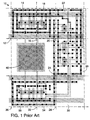
- Fig. 1 shows a portion of an integrated circuit 10 having a substantially regular pattern of transistors and associated electrical interconnections that are amenable to processing with an ion implantation tool positioned by a panelized database.
- the threshold voltages of selected transistors are adjusted by controllably implanting boron ions into appropriate p-channel substrate regions of integrated circuit 10.
- the substrate areas to be doped cover a larger area than the movement range of the fast positioner.
- the slow positioner drives the ion implantation tool into relative alignment with integrated circuit 10 at an origin 12 of a panel 14 (panels shown in dashed lines) after which movement the fast positioner executes the relatively short movements required between the ion implantation tool and integrated circuit 10 to process the substrate areas within panel 14 commanded by the database.
- the slow positioner moves the ion implantation tool into relative alignment with integrated circuit 10 at an origin 16 of a panel 18 after which movement the fast positioner executes the relatively short movements required between the ion implantation tool and integrated circuit 10 to process the substrate areas within panel 18 as commanded by the database.
- interconnect pad 40 is not completely enclosed within a single panel. Fortunately in this instance, interconnect pad 40 requires no ion implantation processing and can be ignored for panelization purposes.
- Database panelization is at best an inefficient, approximate optimization that divides the tool path into several predetermined compartmentalized small movement command clusters that are inherently inefficient because the movements are executed incrementally.
- Panelization also depends on the movement capacities of the particular positioners employed and the type of tool being positioned. For example, the panels assigned to integrated circuit 10 must be delineated in the database not only according to the pattern regularity of integrated circuit 10, but also according to the movement range of the fast positioner and specific target locations assigned to the ion implantation tool. If the tool type is changed, a different positioner type may be required that processes different features at different target locations. Either change would probably require that the database be repanelized to accommodate the new positioner and tool.
- Panelization further requires that each panel within a database must abut adjacent panels within the workpiece without causing a tool operation to straddle or overlap a panel boundary.
- the panelization shown in Fig. 1 may not be suitable because interconnect pad 40 straddles two panels.
- the workpiece includes irregular patterns, such as target locations for drilling holes in an etched circuit board.
- Some workpiece and tool type combinations are simply not conducive to panelization.
- pattern regularity may repeat, albeit at a dimensional distance greater than the movement range of a particular fast positioner. Adapting a fast positioner having a sufficiently large movement range may be counter-productive because of added mass and nonlinearities.
- An object of this invention as defined by independent claims 1 and 11, is, therefore, to provide an improved apparatus and method for cutting a pre-determined hole pattern in at least two circuit boards.
- An advantage of this invention is that it provides an apparatus and a method for performing tool path operations simultaneously on multiple workpieces without requiring a panelized database.
- Another advantage of this invention is that it provides an apparatus and a method for improving the accuracy and throughput of multiple simultaneous tool path operations employing a multi-rate positioning system.
- a multi-rate positioner system of this invention receives unpanelized positioning commands from a database, profiles the commands into half-sine positioning signals, and further processes the half-sine positioning signals into low-frequency and high-frequency positioning signals for actuating respective slow and fast positioners to target locations specified by the database.
- the slow and fast positioners move, without necessarily stopping, in response to a stream of positioning command data while coordinating their individually moving positions to produce temporarily stationary tool positions over target locations defined by the database.
- the multi-rate positioning system reduces the fast positioner movement range requirement while providing significantly increased tool processing throughput without requiring a panelized database.
- the half-sine positioning signal is divided into acceleration and position components.
- High tool processing throughput is achieved by passing the position component through a fourth-order profiling filter that has a fixed delay and produces low-frequency position and acceleration components for driving the slow positioner.
- the unfiltered position and acceleration components are delayed by the same amount as the fixed delay to produce high-frequency position and acceleration components for driving the fast positioner.
- Slow positioner errors caused by nonresponsiveness of the slow positioner to fast stage components fed through the profiling filter are corrected by directing these feedthrough-related errors to the fast positioner as part of the fast positioner command.
- Positioning errors caused by inertia and friction associated with the positioners are corrected by comparing the actual tool position with a commanded tool position in feedback networks that modify the slow and fast stage positioning signals.
- a multi-rate, multi-head positioner embodiment of this invention receives and processes the unpanelized positioning commands as above to actuate the slow positioner and multiple fast positioners that are mounted on the slow positioner to simultaneously position multiple tools relative to target locations on multiple associated workpieces.
- Each of the fast positioners is coupled to a fast stage signal processor that provides corrected position data to each fast stage positioner to compensate for fast stage nonlinearities and workpiece placement, offset, rotation, and dimensional variations among the multiple workpieces.
- the multi-rate, multi-head positioner system reduces workpiece processing cost and improves workpiece processing throughput by simultaneously processing multiple workpieces with a single system. Moreover, processed workpiece rejects are reduced because of the ability to process workpieces having placement, offset, rotation, and dimensional variations.
- a preferred embodiment of the multi-rate, multi-head positioner cuts blind via holes in etched circuit boards ("ECBs") with improved throughput and process yield.
- half of the tools are ultraviolet (“UV”) lasers, which readily cut conductor and dielectric layers, and the other half of the tools are infrared (“IR”) lasers, which readily cut only dielectric layers.
- UV lasers are controlled to cut an upper conductor layer and a portion of an underlying dielectric layer, and the IR lasers are controlled to cut the remaining dielectric layer without cutting through or damaging a second underlying conductor layer.
- the combined laser processing steps have a wide process window for cutting blind via holes in ECBs.
- the throughput is increased by cutting conductor layers in unprocessed ECBs while concurrently cutting dielectric layers in ECBs that have already had their conductor layer cut.
- the process yield is increased by performing a workpiece calibration prior to each cutting step to account for any ECB placement, offset, rotation, and dimensional variations.
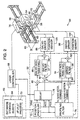
- Fig. 2 shows a multi-stage tool positioner system 50 having positioning command execution capabilities in accordance with this invention.
- Positioner system 50 is described only by way of example with reference to a single-head, laser-based hole cutting system that employs a digital signal processor ("DSP") 52 to control a fast galvanometer positioner stage 54 ("fast stage 54"), a slow X-axis translation stage 56 (“slow stage 56"), and a slow Y-axis translation stage 58 ("slow stage 58") to direct a laser beam 60 to target locations on a single workpiece 62, such as an etched circuit board.
- DSP digital signal processor
- positioner system 50 is configured with single fast stage 54 mounted on slow stage 56 and a single workpiece 62 mounted on slow stage 58
- other configurations of tool positioning systems such as one in which multiple fast stages 54 are mounted on slow stage 56 and multiple workpieces 62 are mounted on slow stage 58, may advantageously employ this invention.
- a system control computer 63 processes a tool path database stored in a database storage subsystem 64.
- the database contains the desired processing parameters for cutting holes and/or profiles with laser beam 60 in workpiece 62.
- the database is conventionally compiled using a tool path generating program, such as SMARTCAMTM manufactured by Camex Manufacturing Technologies located in Eugene, Oregon.
- System control computer 63 conveys parsed portions of the stored database to a laser controller 68 and position control portions of the database as a data stream to a delta process 70.
- Delta process 70 resolves the data stream into delta position ("dx" and "dy”), delta velocity (“dv”), and delta time (“dt”) components for each intended change in the path of laser beam 60 across workpiece 62. Consequently, each movement of laser beam 60 is defined in dx, dy, dv, and dt components that are further processed by a position profiler 72 into a half-sine profiled positioning signal.
- Laser controller 68 is controlled by timing data generated by delta process 70 and further coordinated by a triggering process that synchronizes the firing of a laser 76 to the motion of fast stage 54 and slow stages 56 and 58 according to a synchronization technique, such as one described in U.S. Pat. No. 5,453,594, issued September 26, 1995, for RADIATION BEAM POSITION AND EMISSION COORDINATION SYSTEM, which is assigned to the assignee of this application.
- Delta process 70 generates the dx, dy, dv, and dt components in accordance with a preferred BASIC language signal processing procedure described below with reference to Figs. 3A and 3B.
- limiting values for maximum acceleration (amax), maximum velocity (vmax), and minimum time (tmin) are initialized.
- the limiting values are physical hardware limits imposed by the particular positioner hardware (fast or slow) that is required to move a majority of the distance in response to a particular positioning command. For example, if the movement distance is less than 25 percent of the maximum fast positioner movement range, then the values are set for the fast positioner. Otherwise the values are set for the slow positioner.
- Limiting values for fast stage 54 and slow stages 56 and 58 are: Fast Slow vmax (Meters/Second) 1 0.25 amax (g) 50 1.0 tmin (Milliseconds) 2 20.0
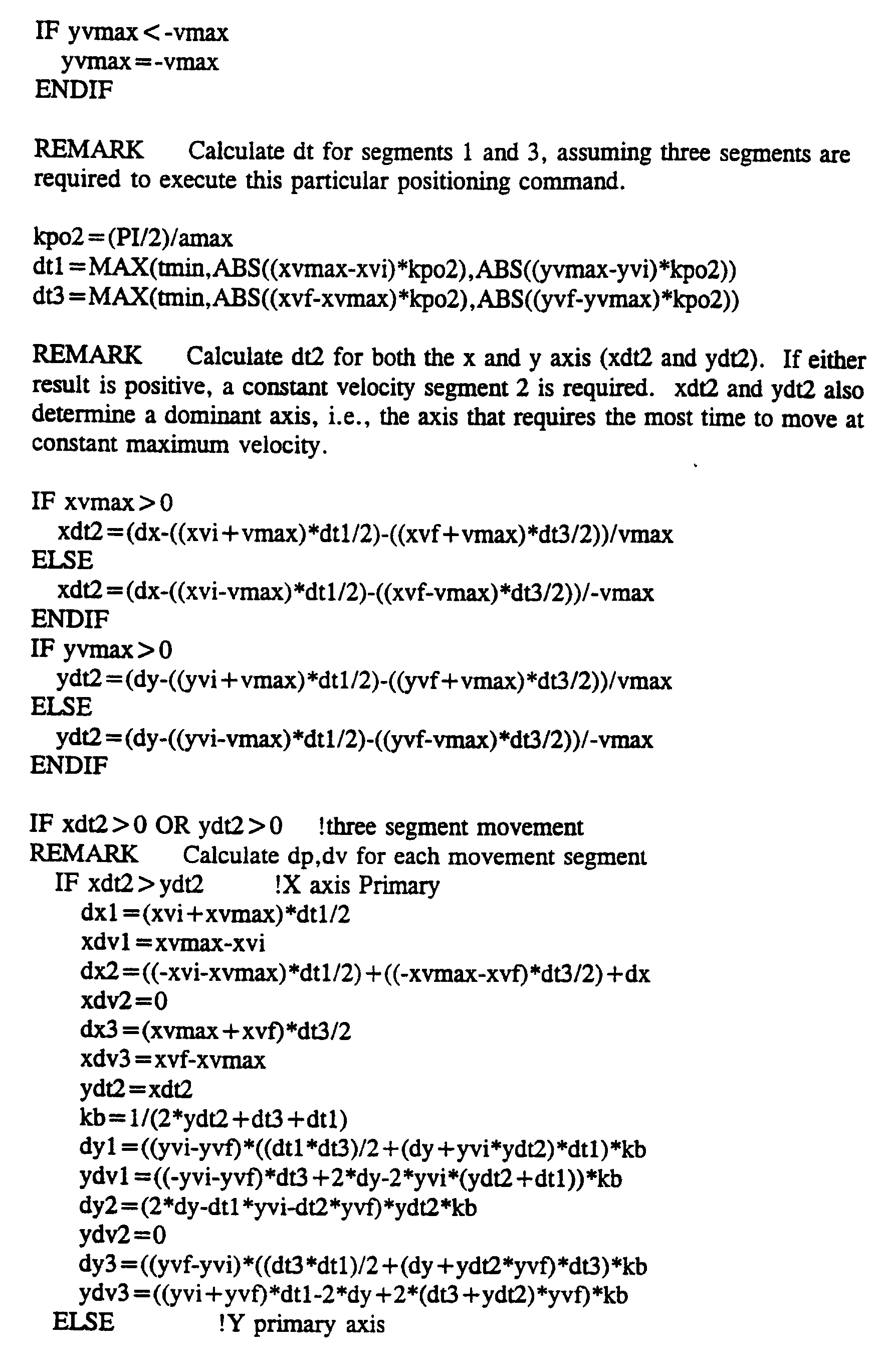
- Procedure gen_move calculates the dx, dy, dv, and dt values required for a positioner stage to move in either two or three movement segments from any initial position and initial velocity to any final position and final velocity.
- All movement segments include some combination of a half-sine profiled acceleration segment ("segment 1”), a constant velocity segment (“segment 2”), and a half-sine profiled deceleration segment (“segment 3").
- segment 1 a half-sine profiled acceleration segment
- segment 2 a constant velocity segment
- segment 3 a half-sine profiled deceleration segment
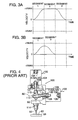
- Fig. 3A when a positioning command is sufficiently large to cause the positioner velocity to reach either +vmax or -vmax, segment 2 is included between segments 1 and 3. Otherwise, as shown in Fig. 3B, a two-segment movement command is executed that includes only segments 1 and 3 (segment 2 equals 0).
- Procedure gen_move generally conforms to, and skilled workers will readily understand, the following BASIC language description.
- the dx, dy, dv, and dt components generated by delta process 70 are further processed by position profiler 72 into the half-sine positioning signal required to move fast stage 54 and slow stages 56 and 58 as commanded by the database.
- positioner acceleration is proportional to motive force
- motive force is proportional to electrical current supplied to a positioner driver such as a linear or rotary servo motor or a galvanometer coil. Therefore, the positioning signal produced by position profiler 72 is a series of "full-spectrum" half-sine profiled acceleration-inducing positioning steps that cause movements such as those shown in Figs. 3A and 3B.
- the full-spectrum bandwidth need only be about 250 Hertz, a bandwidth sufficient to drive a typical galvanometer-driven mirror positioner at its maximum frequency.
- Instantaneous values of the full-spectrum positioning signal are generated by DSP 52 at a rate of about 10,000 points per second by employing the dx, dy, dv, and dt components generated by delta process 70 as variables for a sine value generation program running in DSP 52.
- the dx, dy, dv, and dt components may be employed to address and fetch associated sinusoidal waveform values stored in a sine value lookup table that is incorporated within DSP 52.
- the resulting full-spectrum positioning signal has acceleration and position components that are received by a profiling filter 78 having a constant signal propagation delay and a delay element 79 that compensates in DSP 52 for the constant signal propagation delay of profiling filter 78.
- delay element 79 delays the laser triggering pulses generated by position profiler 72 to coincide with the delayed movements of fast stage 54 and slow stages 56 and 58.
- Profiling filter 78 and delay element 79 also cooperate, as described below, to move slow stages 56 and 58 smoothly over the average position profile while limiting its acceleration to ⁇ 1 g and cooperate to limit fast stage 54 positioning movements to ⁇ 10 millimeters.
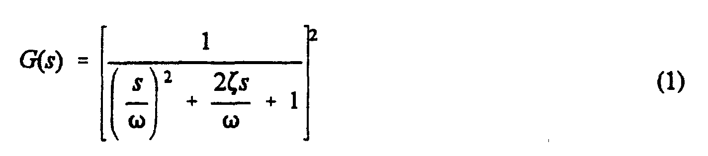
- profiling filter 78 is preferably a fourth-order low-pass filter represented below by Eq. 1.
- ⁇ is the natural, or cutoff, frequency of profiling filter 78 and ⁇ is its damping ratio.
- ⁇ is 38 radians per second and ⁇ equals 0.707.
- the 0.707 value of ⁇ is referred to as the critical damping ratio because it produces a phase lag that is linear with frequency up to the cutoff frequency ⁇ of profiling filter 78.
- the linear phase lag results in a constant time delay for any half-sine positioning signal having a frequency content up to the natural frequency. For the Eq. 1 filter, the time delay equals 4 ⁇ / ⁇ seconds.
- profiling filter 78 produces filtered position command data having a constant time delay with respect to the half-sine positioning signal position component
- the constant time delay is compensated for by delay element 79.
- Delay element 79 is preferably implemented in DSP 52 as a programmed delay in conveying the half-sine positioning signal acceleration and position components from position profiler 72 to fast stage 54 signal processing elements, the first of which are adders 80 and 82. Thereby, half-sine positioning signals directed to fast stage 54 are time synchronized with the filtered position commands directed to slow stages 56 and 58.
- the acceleration component from position profiler 72 is also filtered by profiling filter 78 to provide a filtered acceleration command to adder 80 and a feed forward process 94.
- Adder 80 functions as a high-pass filter by subtracting the filtered acceleration command from the acceleration component of the full-spectrum positioning signal to form a galvo acceleration feed forward signal, which is conveyed to a feed forward process 86.
- the filtered position command from profiling filter 78 and the delayed position component of the half-sine positioning signal are conveyed respectively to adders 90 and 82 for processing and distribution, respectively, to slow stages 56 and 58 and fast stage 54.
- a galvo filter 97 and a servo filter 98 are conventional loop compensation filters that function to keep fast stage 54 and slow stages 56 and 58 stable.
- Profiling filter 78 is implemented by cascading two or more second-order filters having critical damping ratios. As the number of cascaded filters increases beyond two, their cutoff frequencies increase by about the square root of the number of filters (e.g., two filters have cutoffs that are 1.414 times the cutoff for a single filter). Preferably two filters are cascaded to provide good smoothing while keeping the overall filter implementation simple.
- the profiling filter response represented by Eq. 1 can be expressed as a discrete equivalent through a bilinear transformation.
- the resulting digital transfer function is represented below by Eq. 2.
- Gz ( z ) k z 2 + 2 z + 1 2 z 2 + b 1 z + b 2 2
- Eqs. 3 and 4 are determined as represented below in Eq. 5.
- T is the sample period of the filter
- ⁇ is its cutoff frequency
- ⁇ is its damping ratio
- profiling filter 78 For profiling filter 78, the preferred 38 radian per second cutoff frequency (about 6 Hertz) is a very low frequency compared to the 10 kiloHertz rate at which DSP 52 updates positioning data for slow stages 56 and 58. If profiling filter 78 runs at the 10 kiloHertz slow stage update frequency, the discrete filter coefficients become sensitive to roundoff errors because the poles of the discrete filter move close to the unit circle. Therefore, it is preferred that profiling filter 78 run as two second-order filters as represented in Eqs. 3 and 4 to reduce the order of the filter equation and to keep the filter coefficients reasonably controlled.
- Profiling filter 78 also receives the acceleration command from position profiler 72 and generates the filtered acceleration command that is conveyed to servo feed forward process 94 and to adder 80.
- the desired move profile commands are preferably calculated at the 10 kiloHertz updating rate, and the slow stage acceleration and actual (not commanded) position is subtracted therefrom at adders 80 and 82 to produce, respectively, the fast stage acceleration and position command signals.
- the fast stage acceleration command signal is processed through adder 80 and feed forward process 86, while the fast stage position command signal is processed through adder 82 and galvo filter 97.
- the processed fast stage signals are combined in an adder 84 and conveyed to a galvanometer driver 88.
- the slow stage filtered acceleration command is processed through a feed forward process 94, while the slow stage filtered position command is processed through adder 90 and servo filter 98.
- the processed slow stage signals are combined in an adder 92 and conveyed to a linear servo motor driver 96.
- Galvanometer driver 88 provides deflection control current to a pair of mirror deflecting galvanometers in fast stage 54
- servo motor driver 96 provides control current to linear servo motors that control the positioning of slow stages 56 and 58.
- Fig. 4 shows a prior art galvanometer-driven mirror positioner 100 of a type suitable for use as fast stage 54.
- Galvanometer driver 88 (Fig. 2) provides rotational control current on conductors 102 to respective X-axis and Y-axis high-speed response D.C. motors 104 and 106 that rotate shafts 107 in bearings 108 to selectively pivot a pair of mirrors 110 and 112 that deflect laser beam 60 through an optional lens 114 to a predetermined target location on workpiece 62.
- a nonbearing motion positioner such as a piezoelectric element, a voice coil actuator, or other limited angle high-speed positioner device could be used in place of galvanometer-driven mirror positioner 100 in positioner system 50.
- Two signals are combined with the slow and fast stage position commands to reduce positional errors between the commanded position and the actual position of laser beam 60 on workpiece 62.
- the delayed fast stage position command at adder 82 and the filtered slow stage position command at adder 90 represent the ideal signal values required to cause proper positioning of stages 54, 56, and 58.
- practical factors such as gravity, friction, mass, and inaccuracies in the full-spectrum positioning signal generated by position profiler 72 are not contemplated in the unmodified position commands.
- Position sensors 120 and 122 may be well-known types employing rotating capacitor plates, linear and rotary encoder scales, or interferometer motion detectors together with appropriate analog-to-digital and/or digital-to-analog conversion techniques.
- sensed position data of fast stage 54 and slow stages 56 and 58 are generated by position sensors 120 and 122 and subtracted from the commanded position at adder 82 to generate positional difference data that are combined in adder 84 with acceleration data from feed forward process 86.
- sensed position data of slow stages 56 and 58 are generated by position sensor 122 and subtracted from the commanded position at adder 90 to generate positional difference data that are combined in adder 92 with acceleration data from feed forward process 94.
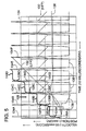
- Fig. 5 graphically shows how fast stage 54 and slow stages 56 and 58 coordinate their movements in response to a representative full-spectrum positioning signal 128 (shown in bold lines), which is divided in DSP 52 (Fig. 2) into a high-frequency position (“HFP") signal portion 130 and a low-frequency position (“LFP”) signal portion 132.
- HFP signal portion 130 represents the AC-coupled, 25-250 Hertz high-passband portion of full-spectrum positioning signal 128, and LFP signal portion 132 represents the direct-coupled, 0-25 Hertz low-passband portion of full-spectrum positioning signal 130.
- Each half-sine profiled positioning step in full-spectrum positioning signal 128 (uniquely identified by a letter suffix, e.g., 128A, 128B, 128C, and 128D) causes a correspondingly identified step in HFP signal portion 130 (e.g., 130A, 130B, 130C, and 130D).
- each positioning step is separated from adjacent positioning steps by about 10 milliseconds, but the time separation, if any, is a function of timing data in the tool path database.
- Fig. 5 further shows a resultant fast stage velocity waveform 134 and a resultant slow stage velocity waveform 136 that reveal, respectively, how fast stage 54 and slow stages 56 and 58 respond to HFP signal portion 130 and LFP signal portion 132.
- HFP signal portions 130A, 130B, 130C, and 130D each include acceleration segments that cause fast stage 54 to undergo sine-profiled velocity changes as represented by corresponding fast velocity waveform pulses 134A, 134B, 134C, and 134D.
- Fast velocity waveform 134 has a baseline 138 that transitions in a negative velocity direction and settles at a value of about -100 millimeters per second. This baseline shift is caused by combining in adder 80 the delayed and filtered acceleration commands.
- HFP signal portion 130 also represents how fast stage 54 responds positionally to each of fast velocity pulses 134.
- the peak fast stage positioning displacement required in this example is about 2.8 millimeters, which is well within the 10-millimeter linear range of a low-mass, galvanometer-driven mirror positioner.
- LFP signal portion 132 also represents how slow stages 56 and 58 respond positionally to slow velocity waveform 136.
- Slow stage velocity waveform 136 transitions in a positive velocity direction and settles at a value of about +100 millimeters per second. In this example, the slow stage position changes linearly with time such that at least one of slow stages 56 and 58 does not stop moving.
- Full-spectrum positioning signal 128 also represents the net positions resulting from the combined fast and slow stage positions represented respectively by waveforms 132 and 130.
- Plateaus 140A, 140B, 140C, and 140D indicate 10 millisecond time periods during which the coordinated position is stationary even though stages 54, 56, and 58 may all be moving. This is clearly shown for plateau 140C, directly under which waveforms 130 and 132 intersect with substantially equal and opposite slopes. Plateaus 140 correspond to time periods during which laser 76 may be triggered to process holes in workpiece 62.
- the above-described coordinated positioning is particularly beneficial for applications such as laser beam hole cutting that requires rapid movement between target locations along a tool path combined with pauses at each target location to fire the laser to cut a hole but, of course, is not limited to that application.
- Fig. 6 shows a multi-head positioner 150 embodiment of this invention in which multiple workpieces 152A, 152B, 152C, ... 152N are simultaneously processed.
- Multi-head positioner 150 employs one each of slow stages 56 and 58 configured such that workpieces 152 are fixtured and carried on Y-axis slow stage 58 and multiple fast stages 154A, 154B, 154C, ... 154N are carried on X-axis slow stage 58.
- slow stages 56 and 58 may be reversed.
- the number N of fast stages 154 carried on slow stage 58 is preferably limited to four, although N may vary with positioner types and applications.
- Each of workpieces 152 has associated with it a processing tool, preferably a laser 156A, 156B, 156C, ... 156N that directs processing energy toward associated fast stages 154A, 154B, 154C, ... 154N by way of associated mirrors 158A, 158B, 158C, ... 158N.
- Fast stages 154 deflect the processing energy to target locations in substantially square, 20 by 20 millimeter processing fields 162A, 162B, 162C, ... 162N located on associated workpieces 152.
- Video cameras 160A, 160B, 160C, ... 160N are positioned on slow stage 56 for viewing associated processing fields 162, sensing the alignments, offsets, rotations, and dimensional variations of workpieces 152, and aiming and focusing lasers 156.
- the same processing pattern is duplicated on workpieces 152 by each of lasers 156 and fast stages 154.
- processing pattern variations may be required to match the pattern to variations among workpiece geometries, scale factors, offsets, rotations, distortions. It may also be necessary to correct for fast stage nonlinearities and "abbe errors" (the degree to which a commanded tool position does not match a sensed target location) introduced by mounting position variations among workpieces 152 mounted on slow stage 58.
- multi-head positioner 150 can compensate for the above-described variations by employing programmable correction factors, described with reference to Figs. 7 and 8, when driving each of fast stages 154.
- Fig. 7 shows how multi-rate positioner DSP 52 (Fig. 2) may be adapted to coordinate the positioning of multiple fast stages 154 and slow stages 56 and 58, resulting in a multi-head DSP 170.
- multi-head DSP 170 receives from system control computer 63 dx, dy, dv, and dt components that are further processed by position profiler 72 into half-sine profiled positioning signals.
- DSP 170 also includes some of the same signal processing elements as DSP 52, namely profiling filter 78, delay element 79, feed forward process 94, servo driver 96, slow stage 56, and position sensor 122. Because Fig. 7 is simplified, only X-axis slow stage 56 processing elements are shown. Skilled workers will understand that corresponding Y-axis elements are implied.
- fast stage signal processors 172A, 172B, 172C, ... 172N each receive fast stage correction data from system control computer 63. In this way, fast stage position commands and current slow stage position data are received by each of fast stage signal processors 172 such that each of fast stages 154 is directed to a common set of target locations that are further positionable by unique error correction data.
- Fig. 8 shows a representative one of fast stage signal processors 172 receiving fast and slow stage positioning data from DSP 170 and correction data from system control computer 63.
- the correction data include slow stage and workpiece related correction data that are conveyed to a geometry correction processor 180 and fast stage linearity and scale factor correction data that are conveyed to a fast stage correction processor 182.
- correction data may be equation- or lookup table-based.
- correction data employed by geometry correction processor 180 and fast stage correction processor are preferably equation-based along lines described in U.S. Pat. No. 4,941,082 for LIGHT BEAM POSITIONING SYSTEM ("the '082 patent"), which is assigned to the assignee of this application.
- Fast stage linearity and scale factor errors are relatively constant and depend mostly on the individual characteristics of fast stages 154. Therefore, fast stage correction processor 182 requires relatively small and infrequent correction data changes. Generating this correction data entails, for example, directing each of fast stages 154 to at least 13 calibration points on an associated calibration target as described in the '082 patent.
- a reflected energy detector senses any differences between the directed and actual target point locations and provides difference data to system control computer 63 for processing. The resulting correction data are conveyed to and stored in each fast stage correction processor 182. Also, any differences between the directed and actual target point locations sensed by associated video cameras 160 are calibrated and compensated for. Slow stage linearity and scale factor errors are also relatively constant and do not, therefore, require frequent correction data changes.
- geometry correction processor 180 requires relatively large correction data changes every time workpieces 152 are changed. Generating this correction data entails, for example, directing slow stages 56 and 58 and each of fast stages 154 to at least two, and preferably four, predetermined calibration targets on each associated workpiece 152. These calibration targets may be, for example, corners, tooling holes, or photoetch targets of an ECB. Each video camera 160 senses differences between the directed and actual calibration target locations and provides difference data to system control computer 63 for processing. The resulting correction data for each workpiece 152 are conveyed to and stored in the associated geometry correction processor 180.
- corrected positioning data for the Y-axis are conveyed from correction processors 180 and 182 to feed forward process 86, galvo driver 88, and fast stage 154.
- Position feedback data are generated by position sensor 120 (as in Fig. 2) and combined for correction in adders 184 and 84. Skilled workers will understand that the same process applies to X-axis fast positioning.
- each fast stage is preferably limited to an 18 by 18 millimeter positioning range within its 20 by 20 millimeter maximum linear positioning range. The remaining 2 millimeters of positioning range is employed for applying the above-described corrections.
- a typical application of this invention is laser cutting of holes, such as blind via holes, in multilayer ECBs.
- Multilayer ECBs are typically manufactured by registering, stacking together, laminating, and pressing multiple 0.05- to 0.08-millimeter thick circuit board layers. Each layer typically contains a different interconnection pad and conductor pattern, which after processing constitutes a complex electrical component mounting and interconnection assembly.
- the component and conductor density trend of ECBs is increasing together with that of integrated circuits. Therefore, the positioning accuracy and dimensional tolerances of holes in ECBs is increasing proportionally.
- the pressing step causes expansion and dimensional variations that lead to scale factor and orthogonality variations among the ECBs.
- fixturing variations can cause dimensional rotation and offset errors among the ECBs.
- ECB thickness variations make it difficult to mechanically drill holes having an accurately predetermined depth.
- This invention solves the above-described problems as follows. Two to four calibration targets are etched at predetermined locations, preferably one at each corner, on each ECB. Video cameras 160 sense differences between the commanded and actual calibration target locations and provide difference data to system control computer 63 for processing. The resulting correction data are conveyed to and stored in geometry correction processor 180.
- Two calibration targets provide sufficient difference data to system control computer 63 to correct for rotation and offset variations among the ECBs.
- Three calibration targets provide sufficient difference data to system control computer 63 to correct for rotation, offset, scale factor, and orthogonality variations among the ECBs.
- Adding a fourth calibration target further allows for correction of trapezoidal distortion in each of the ECBs.
- ECB thickness variations are readily accommodated by the ⁇ 0.13-millimeter ( ⁇ 0.005 inch) laser depth of field.
- blind via holes presents a difficult challenge for any hole processing tool because of the tight depth, diameter, and positioning tolerances involved. This is because blind via holes are typically processed through a first conductor layer (e.g., copper, aluminum, gold, nickel, silver, palladium, tin, and lead), through one or more dielectric layers (e.g., polyimide, FR-4 resin, benzocyclobutene, bismaleimide triazine, cyanate ester-based resin, ceramic), and up to, but not through a second conductor layer. The resulting hole is plated with a conductive material to electrically connect the first and second conductor layers.
- a first conductor layer e.g., copper, aluminum, gold, nickel, silver, palladium, tin, and lead
- dielectric layers e.g., polyimide, FR-4 resin, benzocyclobutene, bismaleimide triazine, cyanate ester-based resin, ceramic
- multi-head positioner 150 is configured as an ECB blind via cutting apparatus in which N equals an even number, such as 2, 4, or 6, but preferably 4.
- Lasers 156A and 156C are UV lasers (wavelength is less than about 355 nanometers), and lasers 156B and 156N are IR lasers (wavelength is in a range from about 1,000 nanometers to about 10,000 nanometers, preferably 9,000 nanometers). Because the UV and IR lasers have substantially different wavelengths, mirrors 158 and optics for fast stages 154 are configured for compatibility with each associated laser's wavelength.
- UV lasers 156A and 156C are capable of cutting both the first conductor layer and the dielectric layer in a suitable manner. However, the laser power levels and pulse repetition rates must be carefully controlled to prevent unacceptable damage to the second conductor layer. This results in a narrow "process window.” Therefore, UV lasers 156A and 156C are controlled to cut through only the first conductor layer and a portion of the dielectric layer, a process that has a wide process window.
- IR lasers 156B and 156N have a wide process window for cutting through the remaining dielectric layer without cutting through or damaging the second conductor layer. However, the first conductor layer must be previously processed.
- the ECB blind via cutting apparatus employs UV lasers 156A and 156C to cut through the first conductor layers of workpieces 152A and 152C and IR lasers 156B and 156N to cut through the dielectric layers on workpieces 152B and 152N.
- multi-head positioner 150 to cut blind via holes proceeds according to the following preferred process. Assume, for example, that an eight workpiece batch of ECBs (ECB1, ECB2, ... and ECB8) is processed.
- the conductor layers are copper and the dielectric layer is FR-4 resin.
- the process for cutting blind via holes in eight workpieces is completed.
- the process may be adapted to concurrently process various numbers of workpieces, and the batch size is not limited to eight, nor to ECBs.
- the time required for UV lasers 156A and 156C to cut through the conductor layers is typically longer than the time required by IR lasers 152B and 152N to cut through the dielectric layer. Therefore, the longer processing time dictates the processing throughput. Because the target locations are substantially identical for all tools on multi-tool positioner 150, the different processing times are accounted for by providing appropriately different laser power levels and pulse repetition rates for the UV and IR lasers.
- UV lasers 154A and 154C have a beam diameter of only about 20 micrometers
- multi-tool positioner 150 must cause the UV beam to follow a spiral or circular path to cut such holes in a conductor layer. Therefore, cutting these relatively large holes takes a proportionally longer time.
- IR lasers 154B and 154N have a beam diameter of about 400 micrometers, which is about 20 times the UV laser beam diameter. Therefore, when cutting these relatively large diameter holes through the dielectric layers, at least some portion of the IR laser beam will cover the entire hole while the UV beam follows the spiral or circular path to cut a hole in a conductor layer. Under these circumstances, the IR laser beams are on the target locations for a relatively longer time and the different effective processing times are again accounted for by providing appropriately different laser power levels and pulse repetition rates for the UV and IR lasers.
- a single laser may be shared among multiple workpieces by employing suitable power splitting devices. It is also envisioned that switchable-wavelength lasers may be employed in this invention.
- This invention provides an improved combination of positioning accuracy, positioning speed, minimized or eliminated stopping time, nonpanelized tool path databases, and minimized fast stage movement range that dramatically improves processing throughput while reducing workpiece rejects caused by dimensional and orientation variations.
- portions of this invention may be implemented differently from the laser beam micro-machining implementation described above.
- many different positioning devices may be employed in different combinations drawn from among galvanometers, voice coils, piezoelectric transducers, stepper motors, and lead screw positioners.
- the DSPs need not be completely digital and may, for example, include any suitable combination of analog and digital subcircuits.
- the positioning signal profiles, spectral bandwidth and amplitudes, and filter characteristics described herein may all be modified to suit the requirements of other positioning applications.
Landscapes
- Physics & Mathematics (AREA)
- Engineering & Computer Science (AREA)
- Optics & Photonics (AREA)
- Mechanical Engineering (AREA)
- Plasma & Fusion (AREA)
- Manufacturing & Machinery (AREA)
- General Physics & Mathematics (AREA)
- Automation & Control Theory (AREA)
- Human Computer Interaction (AREA)
- Microelectronics & Electronic Packaging (AREA)
- Laser Beam Processing (AREA)
- Control Of Position Or Direction (AREA)
- Automatic Tool Replacement In Machine Tools (AREA)
- Drilling And Boring (AREA)
- Jigs For Machine Tools (AREA)
- Turning (AREA)
- Numerical Control (AREA)
- Manufacturing Of Printed Circuit Boards (AREA)
Abstract
Description
- This invention relates to an apparatus and a method for positioning multiple "tools," such as laser beams or other radiation beams, relative to target locations on multiple associated workpieces and, in particular, to a system that accurately coordinates the positioning of the multiple tools and associated target locations with a multi-stage, multi-head positioner.
- A variety of technologies employ tools to micro-machine, or deposit patterns or materials on target locations on a workpiece. For example, micro-dimensioned drills may be used to form a cradle for a micro-dimensioned motor; a micro-dimensioned punch may be used to punch holes in a thin metal plate; a laser may be used to precisely machine or selectively erode metallic, crystalline, or amorphous specimens; and ion beams may be used to selectively implant charged particles into an integrated circuit. All of the above-mentioned processes share a common requirement for accurately and rapidly positioning a pertinent tool to target locations on the workpiece.
- In some high volume production applications, multiple tools are simultaneously positioned relative to multiple corresponding workpieces to improve the processing throughput and reduce total manufacturing cost. One such application employs a multiple spindle drilling machine to simultaneously drill identical sets of holes in multiple circuit boards. Such machines have high throughput but require accurate fixturing of the multiple workpieces, cannot compensate for dimensional differences among the workpieces, and are subject to frequent downtime for drill replacement.
- In a related application, prior workers have employed lasers to machine via holes between the upper layers of a multilayer circuit board. Such machines have high accuracy and do not require drill replacement, but they do not have the high throughput of multiple spindle drilling machines.
- In addition, two emerging, but opposing, requirements exist for coordinating the relative motion between tools and workpieces. Namely, feature sizes are decreasing, causing the need for dimensional precision to increase, while at the same time the overall size of workpieces is increasing. Consequently, the accuracy, size, and speed requirements imposed on tool positioners are taxing the limits of existing positioning systems.
- Existing positioners are typically characterized by low speed and long movement or high speed and short movement. Low-speed and long-movement positioners, such as X-Y translation tables, are characterized by high positional accuracy; whereas high-speed, short-movement positioners, such as galvanometer-driven beam deflectors, are characterized by deflection angle nonlinearities.
- A solution for long-movement, high-speed positioning is described in U.S. Pat. No. 4,532,402 issued July 30, 1985 for METHOD AND APPARATUS FOR POSITIONING A FOCUSED BEAM ON AN INTEGRATED CIRCUIT in which a high-speed short-movement positioner ("fast positioner"), such as a galvanometer, is combined with a long-movement, low-speed, but high-accuracy positioner ("slow positioner") such as an X-Y translation table. The two positioners are capable of combining short and rapid movement with long and accurate movement to accurately and rapidly position a tool, such as a laser beam, to target locations on a workpiece, such as an integrated circuit or an etched circuit board. The combined movement of the two positioners entails first moving the slow positioner to a known location near a target location on the workpiece, stopping the slow positioner, moving the fast positioner to the exact target location, stopping the fast positioner, causing the tool to operate on the target location, and then repeating the process for the next target location.
- However, such a positioning method has serious drawbacks. Clearly, all the starting and stopping causes delays that unduly increase the time required for the tool to process the workpiece. A serious drawback is also imposed upon the computer-based machine tool control file or "database" that typically commands the tool to move to a series of predetermined target locations across the workpiece.
- This drawback can be illustrated by the laser machining of a workpiece such as, for example, an integrated circuit of a type having a regular pattern of small features requiring trimming by a laser beam. The positioner and laser beam will cooperate efficiently if the slow positioner can accurately move the laser beam from pattern to pattern and the fast positioner can rapidly direct the laser beam to all of the small features requiring trimming within each pattern.
- If, however, the size of the largest pattern exceeds the movement range of the fast positioner, the database positioning the tool across the workpiece must be "panelized" into abutting segments that each fit within the movement range of the fast positioner. The above-described trend toward increased dimensional precision and larger workpieces virtually guarantees the need for panelized databases. Panelization allocates the conflicting tasks of short, high-speed positioning and long, high-accuracy positioning into appropriate movement assignments for the fast and slow positioners.
- For example, Fig. 1 shows a portion of an integrated circuit 10 having a substantially regular pattern of transistors and associated electrical interconnections that are amenable to processing with an ion implantation tool positioned by a panelized database. In this example, the threshold voltages of selected transistors are adjusted by controllably implanting boron ions into appropriate p-channel substrate regions of integrated circuit 10. The substrate areas to be doped cover a larger area than the movement range of the fast positioner. Therefore, the slow positioner drives the ion implantation tool into relative alignment with integrated circuit 10 at an origin 12 of a panel 14 (panels shown in dashed lines) after which movement the fast positioner executes the relatively short movements required between the ion implantation tool and integrated circuit 10 to process the substrate areas within panel 14 commanded by the database. After panel 14 is processed, the slow positioner moves the ion implantation tool into relative alignment with integrated circuit 10 at an origin 16 of a panel 18 after which movement the fast positioner executes the relatively short movements required between the ion implantation tool and integrated circuit 10 to process the substrate areas within panel 18 as commanded by the database.
- The above-described process is repeated by stepping through origins 20, 24, 28, 32, and 36 of respective panels 22, 26, 30, 34, and 38 until integrated circuit 10 has been completely processed. Note that an interconnect pad 40 is not completely enclosed within a single panel. Fortunately in this instance, interconnect pad 40 requires no ion implantation processing and can be ignored for panelization purposes.
- Database panelization is at best an inefficient, approximate optimization that divides the tool path into several predetermined compartmentalized small movement command clusters that are inherently inefficient because the movements are executed incrementally.
- Panelization also depends on the movement capacities of the particular positioners employed and the type of tool being positioned. For example, the panels assigned to integrated circuit 10 must be delineated in the database not only according to the pattern regularity of integrated circuit 10, but also according to the movement range of the fast positioner and specific target locations assigned to the ion implantation tool. If the tool type is changed, a different positioner type may be required that processes different features at different target locations. Either change would probably require that the database be repanelized to accommodate the new positioner and tool.
- Panelization further requires that each panel within a database must abut adjacent panels within the workpiece without causing a tool operation to straddle or overlap a panel boundary. In the example of integrated circuit 10, if instead of an ion implantation tool a laser beam tool was employed to process metalization of interconnect pad 40, the panelization shown in Fig. 1 may not be suitable because interconnect pad 40 straddles two panels. The same problem can occur if the workpiece includes irregular patterns, such as target locations for drilling holes in an etched circuit board. Some workpiece and tool type combinations are simply not conducive to panelization. And, of course, pattern regularity may repeat, albeit at a dimensional distance greater than the movement range of a particular fast positioner. Adapting a fast positioner having a sufficiently large movement range may be counter-productive because of added mass and nonlinearities.
- What is needed, therefore, is a high throughput apparatus and method for accurately positioning a wide variety of tools relative to a wide variety of workpieces without requiring a panelized tool path database.
- An object of this invention as defined by independent claims 1 and 11, is, therefore, to provide an improved apparatus and method for cutting a pre-determined hole pattern in at least two circuit boards.
- An advantage of this invention is that it provides an apparatus and a method for performing tool path operations simultaneously on multiple workpieces without requiring a panelized database.
- Another advantage of this invention is that it provides an apparatus and a method for improving the accuracy and throughput of multiple simultaneous tool path operations employing a multi-rate positioning system.
- A multi-rate positioner system of this invention receives unpanelized positioning commands from a database, profiles the commands into half-sine positioning signals, and further processes the half-sine positioning signals into low-frequency and high-frequency positioning signals for actuating respective slow and fast positioners to target locations specified by the database. The slow and fast positioners move, without necessarily stopping, in response to a stream of positioning command data while coordinating their individually moving positions to produce temporarily stationary tool positions over target locations defined by the database. The multi-rate positioning system reduces the fast positioner movement range requirement while providing significantly increased tool processing throughput without requiring a panelized database.
- The half-sine positioning signal is divided into acceleration and position components. High tool processing throughput is achieved by passing the position component through a fourth-order profiling filter that has a fixed delay and produces low-frequency position and acceleration components for driving the slow positioner. The unfiltered position and acceleration components are delayed by the same amount as the fixed delay to produce high-frequency position and acceleration components for driving the fast positioner. Slow positioner errors caused by nonresponsiveness of the slow positioner to fast stage components fed through the profiling filter are corrected by directing these feedthrough-related errors to the fast positioner as part of the fast positioner command. Positioning errors caused by inertia and friction associated with the positioners are corrected by comparing the actual tool position with a commanded tool position in feedback networks that modify the slow and fast stage positioning signals.
- A multi-rate, multi-head positioner embodiment of this invention receives and processes the unpanelized positioning commands as above to actuate the slow positioner and multiple fast positioners that are mounted on the slow positioner to simultaneously position multiple tools relative to target locations on multiple associated workpieces. Each of the fast positioners is coupled to a fast stage signal processor that provides corrected position data to each fast stage positioner to compensate for fast stage nonlinearities and workpiece placement, offset, rotation, and dimensional variations among the multiple workpieces.
- The multi-rate, multi-head positioner system reduces workpiece processing cost and improves workpiece processing throughput by simultaneously processing multiple workpieces with a single system. Moreover, processed workpiece rejects are reduced because of the ability to process workpieces having placement, offset, rotation, and dimensional variations.
- A preferred embodiment of the multi-rate, multi-head positioner cuts blind via holes in etched circuit boards ("ECBs") with improved throughput and process yield. In this embodiment, half of the tools are ultraviolet ("UV") lasers, which readily cut conductor and dielectric layers, and the other half of the tools are infrared ("IR") lasers, which readily cut only dielectric layers. The UV lasers are controlled to cut an upper conductor layer and a portion of an underlying dielectric layer, and the IR lasers are controlled to cut the remaining dielectric layer without cutting through or damaging a second underlying conductor layer. The combined laser processing steps have a wide process window for cutting blind via holes in ECBs. Moreover, the throughput is increased by cutting conductor layers in unprocessed ECBs while concurrently cutting dielectric layers in ECBs that have already had their conductor layer cut. The process yield is increased by performing a workpiece calibration prior to each cutting step to account for any ECB placement, offset, rotation, and dimensional variations.
- Additional objects and advantages of this invention will be apparent from the following detailed description of preferred embodiments thereof, which proceed with reference to the accompanying drawings.
-
- Fig. 1 is a pictorial plan view of an integrated circuit work field panelized for tool processing according to a prior art positioner movement panelization scheme.
- Fig. 2 is a pictorial block diagram of a multi-stage laser beam positioning system of this invention.
- Figs. 3A and 3B are time versus velocity graphs showing respective two- and three-segment positioner velocity profiles processed from positioning commands according to this invention.
- Fig. 4 is a fragmentary pictorial side view showing a prior art galvanometer-driven mirror positioner of a type suitable for use with this invention.
- Fig. 5 is a waveform graph representing fast and slow positioner stage velocities and positions responsive to positioning signals according to this invention.
- Fig. 6 is an oblique pictorial view showing a multi-head laser machining system of this invention.
- Fig. 7 is a simplified electrical block diagram of a digital signal processing system including multiple fast stage signal processors employed in the multi-head laser machining system of Fig. 6.
- Fig. 8 is a simplified electrical block diagram of one of multiple fast stage signal processors employed in the digital signal processing system of Fig. 7.
-
- Fig. 2 shows a multi-stage tool positioner system 50 having positioning command execution capabilities in accordance with this invention. Positioner system 50 is described only by way of example with reference to a single-head, laser-based hole cutting system that employs a digital signal processor ("DSP") 52 to control a fast galvanometer positioner stage 54 ("fast stage 54"), a slow X-axis translation stage 56 ("slow stage 56"), and a slow Y-axis translation stage 58 ("slow stage 58") to direct a laser beam 60 to target locations on a single workpiece 62, such as an etched circuit board. Although positioner system 50 is configured with single fast stage 54 mounted on slow stage 56 and a single workpiece 62 mounted on slow stage 58, other configurations of tool positioning systems, such as one in which multiple fast stages 54 are mounted on slow stage 56 and multiple workpieces 62 are mounted on slow stage 58, may advantageously employ this invention.
- A system control computer 63 processes a tool path database stored in a database storage subsystem 64. The database contains the desired processing parameters for cutting holes and/or profiles with laser beam 60 in workpiece 62. The database is conventionally compiled using a tool path generating program, such as SMARTCAM™ manufactured by Camex Manufacturing Technologies located in Eugene, Oregon. System control computer 63 conveys parsed portions of the stored database to a laser controller 68 and position control portions of the database as a data stream to a delta process 70. Delta process 70 resolves the data stream into delta position ("dx" and "dy"), delta velocity ("dv"), and delta time ("dt") components for each intended change in the path of laser beam 60 across workpiece 62. Consequently, each movement of laser beam 60 is defined in dx, dy, dv, and dt components that are further processed by a position profiler 72 into a half-sine profiled positioning signal.
- Laser controller 68 is controlled by timing data generated by delta process 70 and further coordinated by a triggering process that synchronizes the firing of a laser 76 to the motion of fast stage 54 and slow stages 56 and 58 according to a synchronization technique, such as one described in U.S. Pat. No. 5,453,594, issued September 26, 1995, for RADIATION BEAM POSITION AND EMISSION COORDINATION SYSTEM, which is assigned to the assignee of this application.
- Delta process 70 generates the dx, dy, dv, and dt components in accordance with a preferred BASIC language signal processing procedure described below with reference to Figs. 3A and 3B.
- Before calling the preferred procedure, referred to as "gen_move," limiting values for maximum acceleration (amax), maximum velocity (vmax), and minimum time (tmin) are initialized. The limiting values are physical hardware limits imposed by the particular positioner hardware (fast or slow) that is required to move a majority of the distance in response to a particular positioning command. For example, if the movement distance is less than 25 percent of the maximum fast positioner movement range, then the values are set for the fast positioner. Otherwise the values are set for the slow positioner. Limiting values for fast stage 54 and slow stages 56 and 58 are:
Fast Slow vmax (Meters/Second) 1 0.25 amax (g) 50 1.0 tmin (Milliseconds) 2 20.0 - Procedure gen_move calculates the dx, dy, dv, and dt values required for a positioner stage to move in either two or three movement segments from any initial position and initial velocity to any final position and final velocity.
- All movement segments include some combination of a half-sine profiled acceleration segment ("segment 1"), a constant velocity segment ("segment 2"), and a half-sine profiled deceleration segment ("segment 3"). As shown in Fig. 3A, when a positioning command is sufficiently large to cause the positioner velocity to reach either +vmax or -vmax, segment 2 is included between segments 1 and 3. Otherwise, as shown in Fig. 3B, a two-segment movement command is executed that includes only segments 1 and 3 (segment 2 equals 0). Procedure gen_move generally conforms to, and skilled workers will readily understand, the following BASIC language description.



- Referring again to Fig. 2, the dx, dy, dv, and dt components generated by delta process 70 are further processed by position profiler 72 into the half-sine positioning signal required to move fast stage 54 and slow stages 56 and 58 as commanded by the database. Ideally, positioner acceleration is proportional to motive force, and motive force is proportional to electrical current supplied to a positioner driver such as a linear or rotary servo motor or a galvanometer coil. Therefore, the positioning signal produced by position profiler 72 is a series of "full-spectrum" half-sine profiled acceleration-inducing positioning steps that cause movements such as those shown in Figs. 3A and 3B. The full-spectrum bandwidth need only be about 250 Hertz, a bandwidth sufficient to drive a typical galvanometer-driven mirror positioner at its maximum frequency.
- Instantaneous values of the full-spectrum positioning signal are generated by DSP 52 at a rate of about 10,000 points per second by employing the dx, dy, dv, and dt components generated by delta process 70 as variables for a sine value generation program running in DSP 52. Alternatively, the dx, dy, dv, and dt components may be employed to address and fetch associated sinusoidal waveform values stored in a sine value lookup table that is incorporated within DSP 52.
- The resulting full-spectrum positioning signal has acceleration and position components that are received by a profiling filter 78 having a constant signal propagation delay and a delay element 79 that compensates in DSP 52 for the constant signal propagation delay of profiling filter 78. For example, delay element 79 delays the laser triggering pulses generated by position profiler 72 to coincide with the delayed movements of fast stage 54 and slow stages 56 and 58. Profiling filter 78 and delay element 79 also cooperate, as described below, to move slow stages 56 and 58 smoothly over the average position profile while limiting its acceleration to ± 1 g and cooperate to limit fast stage 54 positioning movements to ± 10 millimeters.
- The position component is received by profiling filter 78 to produce filtered position command data for driving slow stages 56 and 58. Profiling filter 78 is preferably a fourth-order low-pass filter represented below by Eq. 1.In Eq. 1, ω is the natural, or cutoff, frequency of profiling filter 78 and ζ is its damping ratio. Preferably, ω equals 38 radians per second and ζ equals 0.707. The 0.707 value of ζ is referred to as the critical damping ratio because it produces a phase lag that is linear with frequency up to the cutoff frequency ω of profiling filter 78. The linear phase lag results in a constant time delay for any half-sine positioning signal having a frequency content up to the natural frequency. For the Eq. 1 filter, the time delay equals 4ζ/ω seconds.
- Because profiling filter 78 produces filtered position command data having a constant time delay with respect to the half-sine positioning signal position component, the constant time delay is compensated for by delay element 79. Delay element 79 is preferably implemented in DSP 52 as a programmed delay in conveying the half-sine positioning signal acceleration and position components from position profiler 72 to fast stage 54 signal processing elements, the first of which are adders 80 and 82. Thereby, half-sine positioning signals directed to fast stage 54 are time synchronized with the filtered position commands directed to slow stages 56 and 58.
- The acceleration component from position profiler 72 is also filtered by profiling filter 78 to provide a filtered acceleration command to adder 80 and a feed forward process 94. Adder 80 functions as a high-pass filter by subtracting the filtered acceleration command from the acceleration component of the full-spectrum positioning signal to form a galvo acceleration feed forward signal, which is conveyed to a feed forward process 86. Likewise, the filtered position command from profiling filter 78 and the delayed position component of the half-sine positioning signal are conveyed respectively to adders 90 and 82 for processing and distribution, respectively, to slow stages 56 and 58 and fast stage 54. A galvo filter 97 and a servo filter 98 are conventional loop compensation filters that function to keep fast stage 54 and slow stages 56 and 58 stable.
- Profiling filter 78 is implemented by cascading two or more second-order filters having critical damping ratios. As the number of cascaded filters increases beyond two, their cutoff frequencies increase by about the square root of the number of filters (e.g., two filters have cutoffs that are 1.414 times the cutoff for a single filter). Preferably two filters are cascaded to provide good smoothing while keeping the overall filter implementation simple.
- The profiling filter response represented by Eq. 1 can be expressed as a discrete equivalent through a bilinear transformation. The resulting digital transfer function is represented below by Eq. 2.
- The time-domain equations for filter outputs yk and wk, given prior inputs and outputs, are represented below by Eqs. 3 and 4.
- The coefficients in Eqs. 3 and 4 are determined as represented below in Eq. 5.In Eq. 5, T is the sample period of the filter, ω is its cutoff frequency, and ζ is its damping ratio.

- For profiling filter 78, the preferred 38 radian per second cutoff frequency (about 6 Hertz) is a very low frequency compared to the 10 kiloHertz rate at which DSP 52 updates positioning data for slow stages 56 and 58. If profiling filter 78 runs at the 10 kiloHertz slow stage update frequency, the discrete filter coefficients become sensitive to roundoff errors because the poles of the discrete filter move close to the unit circle. Therefore, it is preferred that profiling filter 78 run as two second-order filters as represented in Eqs. 3 and 4 to reduce the order of the filter equation and to keep the filter coefficients reasonably controlled. Profiling filter 78 also receives the acceleration command from position profiler 72 and generates the filtered acceleration command that is conveyed to servo feed forward process 94 and to adder 80.
- The desired move profile commands are preferably calculated at the 10 kiloHertz updating rate, and the slow stage acceleration and actual (not commanded) position is subtracted therefrom at adders 80 and 82 to produce, respectively, the fast stage acceleration and position command signals.
- The fast stage acceleration command signal is processed through adder 80 and feed forward process 86, while the fast stage position command signal is processed through adder 82 and galvo filter 97. The processed fast stage signals are combined in an adder 84 and conveyed to a galvanometer driver 88.
- Likewise, the slow stage filtered acceleration command is processed through a feed forward process 94, while the slow stage filtered position command is processed through adder 90 and servo filter 98. The processed slow stage signals are combined in an adder 92 and conveyed to a linear servo motor driver 96.
- Galvanometer driver 88 provides deflection control current to a pair of mirror deflecting galvanometers in fast stage 54, and servo motor driver 96 provides control current to linear servo motors that control the positioning of slow stages 56 and 58.
- Fig. 4 shows a prior art galvanometer-driven mirror positioner 100 of a type suitable for use as fast stage 54. Galvanometer driver 88 (Fig. 2) provides rotational control current on conductors 102 to respective X-axis and Y-axis high-speed response D.C. motors 104 and 106 that rotate shafts 107 in bearings 108 to selectively pivot a pair of mirrors 110 and 112 that deflect laser beam 60 through an optional lens 114 to a predetermined target location on workpiece 62.
- Alternatively, a nonbearing motion positioner, such as a piezoelectric element, a voice coil actuator, or other limited angle high-speed positioner device could be used in place of galvanometer-driven mirror positioner 100 in positioner system 50.
- Likewise with reference to Fig. 2, alternative accurate rotary or linear positioner mechanisms may be substituted for the linear servo motors driving slow stages 56 and 58. However, in positioner system 50, linear motors that preferentially respond to the slow stage position command are preferred.
- Two signals are combined with the slow and fast stage position commands to reduce positional errors between the commanded position and the actual position of laser beam 60 on workpiece 62. The delayed fast stage position command at adder 82 and the filtered slow stage position command at adder 90 represent the ideal signal values required to cause proper positioning of stages 54, 56, and 58. However, practical factors such as gravity, friction, mass, and inaccuracies in the full-spectrum positioning signal generated by position profiler 72 are not contemplated in the unmodified position commands.
- The practical factors are accounted for by sensing the actual positions of stages 54, 56, and 58 with position sensors 120 and 122 to provide predictive position feedback data to adders 82 and 90 in DSP 52. Note that adder 82 in the fast stage positioning path receives position feedback data from both position sensors 120 and 122. Position sensors 120 and 122 may be well-known types employing rotating capacitor plates, linear and rotary encoder scales, or interferometer motion detectors together with appropriate analog-to-digital and/or digital-to-analog conversion techniques.
- As laser beam 60 undergoes movement across workpiece 62, the sensed beam position is continuously compared to the commanded beam position, with the positional difference representing a degree to which the practical factors have caused positioning errors. In particular, sensed position data of fast stage 54 and slow stages 56 and 58 are generated by position sensors 120 and 122 and subtracted from the commanded position at adder 82 to generate positional difference data that are combined in adder 84 with acceleration data from feed forward process 86. Likewise, sensed position data of slow stages 56 and 58 are generated by position sensor 122 and subtracted from the commanded position at adder 90 to generate positional difference data that are combined in adder 92 with acceleration data from feed forward process 94.
- Fig. 5 graphically shows how fast stage 54 and slow stages 56 and 58 coordinate their movements in response to a representative full-spectrum positioning signal 128 (shown in bold lines), which is divided in DSP 52 (Fig. 2) into a high-frequency position ("HFP") signal portion 130 and a low-frequency position ("LFP") signal portion 132. HFP signal portion 130 represents the AC-coupled, 25-250 Hertz high-passband portion of full-spectrum positioning signal 128, and LFP signal portion 132 represents the direct-coupled, 0-25 Hertz low-passband portion of full-spectrum positioning signal 130.
- Each half-sine profiled positioning step in full-spectrum positioning signal 128 (uniquely identified by a letter suffix, e.g., 128A, 128B, 128C, and 128D) causes a correspondingly identified step in HFP signal portion 130 (e.g., 130A, 130B, 130C, and 130D). In this example, each positioning step is separated from adjacent positioning steps by about 10 milliseconds, but the time separation, if any, is a function of timing data in the tool path database.
- Fig. 5 further shows a resultant fast stage velocity waveform 134 and a resultant slow stage velocity waveform 136 that reveal, respectively, how fast stage 54 and slow stages 56 and 58 respond to HFP signal portion 130 and LFP signal portion 132.
- In particular, HFP signal portions 130A, 130B, 130C, and 130D each include acceleration segments that cause fast stage 54 to undergo sine-profiled velocity changes as represented by corresponding fast velocity waveform pulses 134A, 134B, 134C, and 134D. Fast velocity waveform 134 has a baseline 138 that transitions in a negative velocity direction and settles at a value of about -100 millimeters per second. This baseline shift is caused by combining in adder 80 the delayed and filtered acceleration commands.
- HFP signal portion 130 also represents how fast stage 54 responds positionally to each of fast velocity pulses 134. The peak fast stage positioning displacement required in this example is about 2.8 millimeters, which is well within the 10-millimeter linear range of a low-mass, galvanometer-driven mirror positioner.
- LFP signal portion 132 also represents how slow stages 56 and 58 respond positionally to slow velocity waveform 136. Slow stage velocity waveform 136 transitions in a positive velocity direction and settles at a value of about +100 millimeters per second. In this example, the slow stage position changes linearly with time such that at least one of slow stages 56 and 58 does not stop moving.
- Full-spectrum positioning signal 128 also represents the net positions resulting from the combined fast and slow stage positions represented respectively by waveforms 132 and 130. Plateaus 140A, 140B, 140C, and 140D indicate 10 millisecond time periods during which the coordinated position is stationary even though stages 54, 56, and 58 may all be moving. This is clearly shown for plateau 140C, directly under which waveforms 130 and 132 intersect with substantially equal and opposite slopes. Plateaus 140 correspond to time periods during which laser 76 may be triggered to process holes in workpiece 62.
- The above-described coordinated positioning is particularly beneficial for applications such as laser beam hole cutting that requires rapid movement between target locations along a tool path combined with pauses at each target location to fire the laser to cut a hole but, of course, is not limited to that application.
- Fig. 6 shows a multi-head positioner 150 embodiment of this invention in which multiple workpieces 152A, 152B, 152C, ... 152N are simultaneously processed. (Hereafter multiple elements are referred to collectively without the letter suffix, e.g., "workpieces 152"). Multi-head positioner 150 employs one each of slow stages 56 and 58 configured such that workpieces 152 are fixtured and carried on Y-axis slow stage 58 and multiple fast stages 154A, 154B, 154C, ... 154N are carried on X-axis slow stage 58. Of course, the roles of slow stages 56 and 58 may be reversed.
- As the number of fast stages 154 carried on slow stage 58 increases, their accumulated mass becomes increasingly difficult to accelerate. Therefore, the number N of fast stages 154 carried on slow stage 58 is preferably limited to four, although N may vary with positioner types and applications.
- Each of workpieces 152 has associated with it a processing tool, preferably a laser 156A, 156B, 156C, ... 156N that directs processing energy toward associated fast stages 154A, 154B, 154C, ... 154N by way of associated mirrors 158A, 158B, 158C, ... 158N. Fast stages 154 deflect the processing energy to target locations in substantially square, 20 by 20 millimeter processing fields 162A, 162B, 162C, ... 162N located on associated workpieces 152.
- Video cameras 160A, 160B, 160C, ... 160N are positioned on slow stage 56 for viewing associated processing fields 162, sensing the alignments, offsets, rotations, and dimensional variations of workpieces 152, and aiming and focusing lasers 156.
- In the preferred embodiment, the same processing pattern is duplicated on workpieces 152 by each of lasers 156 and fast stages 154. However, in some processing applications, processing pattern variations may be required to match the pattern to variations among workpiece geometries, scale factors, offsets, rotations, distortions. It may also be necessary to correct for fast stage nonlinearities and "abbe errors" (the degree to which a commanded tool position does not match a sensed target location) introduced by mounting position variations among workpieces 152 mounted on slow stage 58. Unlike prior multi-spindle drilling machines, multi-head positioner 150 can compensate for the above-described variations by employing programmable correction factors, described with reference to Figs. 7 and 8, when driving each of fast stages 154.
- Fig. 7 shows how multi-rate positioner DSP 52 (Fig. 2) may be adapted to coordinate the positioning of multiple fast stages 154 and slow stages 56 and 58, resulting in a multi-head DSP 170. In like manner to DSP 52, multi-head DSP 170 receives from system control computer 63 dx, dy, dv, and dt components that are further processed by position profiler 72 into half-sine profiled positioning signals. DSP 170 also includes some of the same signal processing elements as DSP 52, namely profiling filter 78, delay element 79, feed forward process 94, servo driver 96, slow stage 56, and position sensor 122. Because Fig. 7 is simplified, only X-axis slow stage 56 processing elements are shown. Skilled workers will understand that corresponding Y-axis elements are implied.
- Only a single system control computer 63 is required to drive slow stages 56 and 58 and N fast stages 154. Multiple fast stage signal processors 172A, 172B, 172C, ... 172N each receive fast stage correction data from system control computer 63. In this way, fast stage position commands and current slow stage position data are received by each of fast stage signal processors 172 such that each of fast stages 154 is directed to a common set of target locations that are further positionable by unique error correction data.
- Fig. 8 shows a representative one of fast stage signal processors 172 receiving fast and slow stage positioning data from DSP 170 and correction data from system control computer 63. The correction data include slow stage and workpiece related correction data that are conveyed to a geometry correction processor 180 and fast stage linearity and scale factor correction data that are conveyed to a fast stage correction processor 182.
- The correction data may be equation- or lookup table-based. However, correction data employed by geometry correction processor 180 and fast stage correction processor are preferably equation-based along lines described in U.S. Pat. No. 4,941,082 for LIGHT BEAM POSITIONING SYSTEM ("the '082 patent"), which is assigned to the assignee of this application.
- Fast stage linearity and scale factor errors are relatively constant and depend mostly on the individual characteristics of fast stages 154. Therefore, fast stage correction processor 182 requires relatively small and infrequent correction data changes. Generating this correction data entails, for example, directing each of fast stages 154 to at least 13 calibration points on an associated calibration target as described in the '082 patent. A reflected energy detector senses any differences between the directed and actual target point locations and provides difference data to system control computer 63 for processing. The resulting correction data are conveyed to and stored in each fast stage correction processor 182. Also, any differences between the directed and actual target point locations sensed by associated video cameras 160 are calibrated and compensated for. Slow stage linearity and scale factor errors are also relatively constant and do not, therefore, require frequent correction data changes.
- On the other hand, slow stage and workpiece related errors are relatively variable and depend mostly on workpiece placement, offset, rotation, and dimensional variations among workpieces 152. Therefore, geometry correction processor 180 requires relatively large correction data changes every time workpieces 152 are changed. Generating this correction data entails, for example, directing slow stages 56 and 58 and each of fast stages 154 to at least two, and preferably four, predetermined calibration targets on each associated workpiece 152. These calibration targets may be, for example, corners, tooling holes, or photoetch targets of an ECB. Each video camera 160 senses differences between the directed and actual calibration target locations and provides difference data to system control computer 63 for processing. The resulting correction data for each workpiece 152 are conveyed to and stored in the associated geometry correction processor 180.
- For each fast stage signal processor 172, corrected positioning data for the Y-axis are conveyed from correction processors 180 and 182 to feed forward process 86, galvo driver 88, and fast stage 154. Position feedback data are generated by position sensor 120 (as in Fig. 2) and combined for correction in adders 184 and 84. Skilled workers will understand that the same process applies to X-axis fast positioning.
- In applying the correction data to fast stages 154, each fast stage is preferably limited to an 18 by 18 millimeter positioning range within its 20 by 20 millimeter maximum linear positioning range. The remaining 2 millimeters of positioning range is employed for applying the above-described corrections.
- The foregoing describes signal processing for a single axis of motion for each of the fast and slow positioner stages. Skilled workers will readily understand how to replicate the signal processing to coordinate the motion of both axes, both stages, and single or multiple fast positioners.
- A typical application of this invention is laser cutting of holes, such as blind via holes, in multilayer ECBs. Multilayer ECBs are typically manufactured by registering, stacking together, laminating, and pressing multiple 0.05- to 0.08-millimeter thick circuit board layers. Each layer typically contains a different interconnection pad and conductor pattern, which after processing constitutes a complex electrical component mounting and interconnection assembly. The component and conductor density trend of ECBs is increasing together with that of integrated circuits. Therefore, the positioning accuracy and dimensional tolerances of holes in ECBs is increasing proportionally.
- Unfortunately, the pressing step causes expansion and dimensional variations that lead to scale factor and orthogonality variations among the ECBs. Moreover, when multiple ECBs (workpieces 152) are attached to slow stage 58, fixturing variations can cause dimensional rotation and offset errors among the ECBs. Adding to that, ECB thickness variations make it difficult to mechanically drill holes having an accurately predetermined depth.
- This invention solves the above-described problems as follows. Two to four calibration targets are etched at predetermined locations, preferably one at each corner, on each ECB. Video cameras 160 sense differences between the commanded and actual calibration target locations and provide difference data to system control computer 63 for processing. The resulting correction data are conveyed to and stored in geometry correction processor 180.
- Two calibration targets provide sufficient difference data to system control computer 63 to correct for rotation and offset variations among the ECBs. Three calibration targets provide sufficient difference data to system control computer 63 to correct for rotation, offset, scale factor, and orthogonality variations among the ECBs. Adding a fourth calibration target further allows for correction of trapezoidal distortion in each of the ECBs.
- ECB thickness variations are readily accommodated by the ±0.13-millimeter (±0.005 inch) laser depth of field.
- Processing blind via holes presents a difficult challenge for any hole processing tool because of the tight depth, diameter, and positioning tolerances involved. This is because blind via holes are typically processed through a first conductor layer (e.g., copper, aluminum, gold, nickel, silver, palladium, tin, and lead), through one or more dielectric layers (e.g., polyimide, FR-4 resin, benzocyclobutene, bismaleimide triazine, cyanate ester-based resin, ceramic), and up to, but not through a second conductor layer. The resulting hole is plated with a conductive material to electrically connect the first and second conductor layers.
- Referring again to Fig. 6, multi-head positioner 150 is configured as an ECB blind via cutting apparatus in which N equals an even number, such as 2, 4, or 6, but preferably 4. Lasers 156A and 156C are UV lasers (wavelength is less than about 355 nanometers), and lasers 156B and 156N are IR lasers (wavelength is in a range from about 1,000 nanometers to about 10,000 nanometers, preferably 9,000 nanometers). Because the UV and IR lasers have substantially different wavelengths, mirrors 158 and optics for fast stages 154 are configured for compatibility with each associated laser's wavelength.
- UV lasers 156A and 156C are capable of cutting both the first conductor layer and the dielectric layer in a suitable manner. However, the laser power levels and pulse repetition rates must be carefully controlled to prevent unacceptable damage to the second conductor layer. This results in a narrow "process window." Therefore, UV lasers 156A and 156C are controlled to cut through only the first conductor layer and a portion of the dielectric layer, a process that has a wide process window.
- IR lasers 156B and 156N have a wide process window for cutting through the remaining dielectric layer without cutting through or damaging the second conductor layer. However, the first conductor layer must be previously processed.
- The ECB blind via cutting apparatus employs UV lasers 156A and 156C to cut through the first conductor layers of workpieces 152A and 152C and IR lasers 156B and 156N to cut through the dielectric layers on workpieces 152B and 152N.
- Using multi-head positioner 150 to cut blind via holes proceeds according to the following preferred process. Assume, for example, that an eight workpiece batch of ECBs (ECB1, ECB2, ... and ECB8) is processed. Preferably, the conductor layers are copper and the dielectric layer is FR-4 resin.
- Mount unprocessed ECB1 and ECB2 on slow stage 58 in workpiece positions 152A and 152C for processing by respective UV lasers 156A and 156C.
- Perform a workpiece calibration process as follows:
- direct slow stages 56 and 58 and fast stages 154 to calibration target locations on the ECBs;
- sense with video cameras 160 differences between the directed and actual target locations and provide difference data to system control computer 63 for processing; and
- store correction data for the ECBs in associated fast stage signal processors 172.
-
- Position slow stages 56 and 58 and fast stages 154 to a predetermined set of target locations such that UV lasers 156A and 156C cut through the first conductor layers on ECB1 and ECB2 at the set of target locations.
- Remount semiprocessed ECB1 and ECB2 on slow stage 58 in workpiece positions 152B and 152N for processing by respective IR lasers 156B and 156N.
- Mount unprocessed ECB3 and ECB4 on slow stage 58 in workpiece positions 152A and 152C for processing by respective UV lasers 156A and 156C.
- Perform the workpiece calibration process.
- Position slow stages 56 and 58 and fast stages 154 such that UV lasers 156A and 156C cut through the first conductor layers at the target locations on ECB3 and ECB4 while IR lasers 156B and 156D concurrently cut through the dielectric layers at the target locations on ECB1 and ECB2.
- Unmount processed ECB1 and ECB2 from slow stage 58.
- Remount semiprocessed ECB3 and ECB4 on slow stage 58 in workpiece positions 152B and 152N for processing by respective IR lasers 156B and 156N.
- Mount unprocessed ECB5 and ECB6 on slow stage 58 in workpiece positions 152A and 152C for processing by respective UV lasers 156A and 156C.
- Perform the workpiece calibration process.
- Position slow stages 56 and 58 and fast stages 154 such that UV lasers 156A and 156C cut through the first conductor layers at the target locations on ECB5 and ECB6 while IR lasers 156B and 156D concurrently cut through the dielectric layers at the target locations on ECB3 and ECB4.
- Unmount processed ECB3 and ECB4 from slow stage 58.
- Remount semiprocessed ECB5 and ECB6 on slow stage 58 in workpiece positions 152B and 152N for processing by respective IR lasers 156B and 156N.
- Mount unprocessed ECB7 and ECB8 on slow stage 58 in workpiece positions 152A and 152C for processing by respective UV lasers 156A and 156C.
- Perform the workpiece calibration process.
- Position slow stages 56 and 58 and fast stages 154 such that UV lasers 156A and 156C cut through the first conductor layers at the target locations on ECB7 and ECB8 while IR lasers 156B and 156D concurrently cut through the dielectric layers at the target locations on ECB5 and ECB6.
- Unmount processed ECB5 and ECB6 from slow stage 58.
- Remount semiprocessed ECB7 and ECB8 on slow stage 58 in workpiece positions 152B and 152N for processing by respective IR lasers 156B and 156N.
- Perform the workpiece calibration process.
- Position slow stages 56 and 58 and fast stages 154 such that IR lasers 156B and 156D cut through the dielectric layers at the target locations on ECB8 and ECB8.
- Unmount processed ECB7 and ECB8 from slow stage 58.
- The process for cutting blind via holes in eight workpieces is completed. Of course, the process may be adapted to concurrently process various numbers of workpieces, and the batch size is not limited to eight, nor to ECBs.
- The time required for UV lasers 156A and 156C to cut through the conductor layers is typically longer than the time required by IR lasers 152B and 152N to cut through the dielectric layer. Therefore, the longer processing time dictates the processing throughput. Because the target locations are substantially identical for all tools on multi-tool positioner 150, the different processing times are accounted for by providing appropriately different laser power levels and pulse repetition rates for the UV and IR lasers.
- Some applications require cutting relatively large hole diameters of about 200 micrometers or less. Because UV lasers 154A and 154C have a beam diameter of only about 20 micrometers, multi-tool positioner 150 must cause the UV beam to follow a spiral or circular path to cut such holes in a conductor layer. Therefore, cutting these relatively large holes takes a proportionally longer time. However, IR lasers 154B and 154N have a beam diameter of about 400 micrometers, which is about 20 times the UV laser beam diameter. Therefore, when cutting these relatively large diameter holes through the dielectric layers, at least some portion of the IR laser beam will cover the entire hole while the UV beam follows the spiral or circular path to cut a hole in a conductor layer. Under these circumstances, the IR laser beams are on the target locations for a relatively longer time and the different effective processing times are again accounted for by providing appropriately different laser power levels and pulse repetition rates for the UV and IR lasers.
- If suitable laser power is available, a single laser may be shared among multiple workpieces by employing suitable power splitting devices. It is also envisioned that switchable-wavelength lasers may be employed in this invention.
- This invention provides an improved combination of positioning accuracy, positioning speed, minimized or eliminated stopping time, nonpanelized tool path databases, and minimized fast stage movement range that dramatically improves processing throughput while reducing workpiece rejects caused by dimensional and orientation variations.
- Skilled workers will recognize that portions of this invention may be implemented differently from the laser beam micro-machining implementation described above. For example, many different positioning devices may be employed in different combinations drawn from among galvanometers, voice coils, piezoelectric transducers, stepper motors, and lead screw positioners. The DSPs need not be completely digital and may, for example, include any suitable combination of analog and digital subcircuits. Of course, the positioning signal profiles, spectral bandwidth and amplitudes, and filter characteristics described herein may all be modified to suit the requirements of other positioning applications.
- It will be obvious to skilled workers that many other changes may be made to the details of the above-described embodiments of this invention without departing from the underlying principles thereof. The scope of the present invention should, therefore, be determined only by the following claims.
Claims (20)
- A method for cutting a pre-determined hole pattern in at least first and second substantially identical circuit boards (152A-152N) each having at least a first conductor layer, a dielectric layer, and a second conductor layer, comprising:generating a first laser beam having a first wavelength;providing a first movable slow positioner stage (58); andproviding a first movable fast positioner stage (154A), the method being characterised by:generating at least a second laser beam having a second wavelength;mounting the circuit boards (152A-152N) on the first movable slow positioner stage (58), the first movable slow positioner stage (58) being movable so as to effect a large range of relative movement between the laser beams and the circuit boards (152A-152N);providing at least a second fast movable positioner stage (154B-154N) and a second movable slow positioner stage (56), the at least first and second movable fast position stages (154A-154N) being mounted on the second movable slow positioner stage (56) and being movable so as to effect small ranges of relative movement between the laser beams and associated ones of the circuit boards (152A-152N); andco-ordinating the said large and small ranges of relative movement such that the first laser beam cuts the pre-determined hole pattern in the first conductor layer of the first circuit board while the second laser beam cuts the predetermined hole pattern in the dielectric layer of the second circuit board.
- The method of claim 1 further comprising:generating slow and fast movement-controlling signals for positioning the laser beams relative to the circuit boards (152A-152N) in accordance with the predetermined hole pattern;driving the slow movable positioner stages (56,58) within the large range of relative movement in response to the slow movement-controlling signals; anddriving the multiple movable fast positioner stages (154A-154N) within the small ranges of relative movement in response to the fast movement-controlling signals.
- The method of claim 1 or 2 in which the second movable slow positioner stage (56) includes an X-axis translation stage and the first movable slow positioner stage (58) includes a Y-axis translation stage.
- The method of any preceding claim in which the first laser beam is generated by an ultra-violet laser (156A) and the second laser beam is generated by an infrared laser (156B).
- The method of any preceding claim in which the first wavelength is less than about 355 nanometers and the second wavelength is in a range from about 1,000 nanometers to about 10,000 nanometers.
- The method of any preceding claim in which the co-ordinating step is carried out such that the first and second laser beams concurrently cut the first conductor layer of the first circuit board and the dielectric layer of the second circuit board.
- The method of any preceding claim further comprising:identifying for each of the circuit boards (152A-152N) a substantially identical set of calibration targets;sensing the positioning of the sets of calibration targets to identify positioning errors associated with each of the circuit boards;processing the sensed positioning errors; andcorrecting the small ranges of relative movement to compensate for the positioning errors such that each of the laser beams are accurately positionable to the determined hole pattern on an associated circuit board (152A-152N).
- The method of claim 7 in which at least two calibration targets are identified and the positioning errors include rotation and offset variations among the circuit boards (152A-152N).
- The method of claim 8 in which at least three calibration targets are identified and the positioning errors include scale factor and orthogonality variations among the circuit boards (152A-152N).
- The method of claim 9 in which at least four calibration targets are identified and the positioning errors include trapezoidal distortion variations among the circuit boards (152A-152N).
- A system for cutting a predetermined hole pattern in at least first and second substantially identical circuit boards (152A-152N) each having at least a first conductor layer, a dielectric layer, and a second conductor layer, comprising:a first laser (156A) generating a first laser beam having a first wavelength;a first movable slow positioner stage (58); anda first movable fast positioner stage (154A). the system being characterised by:at least a second laser (156B-156N), generating a second laser beam having a second wavelength;the first movable slow positioner stage (58) having the circuit boards (152A-152N) mounted thereon, the first movable slow positioner stage (58) being movable so as to effect a large range of relative movement between the laser beams and the circuit boards (152A-152N);at least a second movable fast positioner stage (154B-154N). the at least first and second movable fast positioner stages (154A-154N) being movable so as to effect small ranges of relative movement between the laser beams and associated ones of the circuit boards (152A-152N);a second movable slow positioner stage (56) with the at least first and second movable fast positioner stages (154A-154N) mounted thereon, the second movable slow positioner stage (56) also being movable so as to effect a large range of relative movement between the laser beams and the circuit boards (152A-152N); anda signal processor co-ordinating the said large and small ranges of relative movement such that the first laser beam cuts the predetermined hole pattern in the first conductor layer of the first circuit board while the second laser beam cuts the predetermined hole pattern in the dielectric layer of the second circuit board.
- The system of claim 11, in which the signal processor generates slow and fast movement-controlling signals for positioning the laser beams relative to the circuit board (152A-152N) in accordance with the predetennined hole pattern, drives the first and second movable slow positioner stages (56, 58) in response to the slow movement-controlling signal and drives the movable fast positioner stages (154A-154N) in response to the fast movement-controlling signals.
- The system of claims 11 or 12 in which the second movable slow positioner stage (56) includes an X-axis translation stage and the first movable slow positioner stage (58) includes a Y-axis translation stage.
- The system of any one of claims 11 to 13 in which the first laser beam is generated by an ultra-violet laser (156A), and the second laser beam is generated by an infrared laser (156B).
- The system of any one of claims 11 to 14 in which the first wavelength is less than about 355 nanometers and the second wavelength is in a range from about 1,000 nanometers to about 10,000 nanometers.
- The system of any one of claims 11 to 15, in which the first laser beam cuts the first conductor layer of the first circuit board (152A) and the second laser beam concurrently cuts the dielectric layer of the second circuit board (152B).
- The system of any one of claims 11 to 16 further comprising:a substantially identical set of calibration targets on each of the circuit boards (152A-152N);at least one video camera (160A-160N) sensing the position of the sets of calibration targets to identify positioning errors associated with each of the circuit boards (152A-152N);a computer (63) processing the sensed positioning errors to generate correction data; andfast stage signal processors (172A-172N) receiving the correction data and correcting the fast movement-controlling signals to compensate for the positioning errors such that each of the laser beams are accurately positionable to the predetermined hole pattern on an associated circuit board.
- A system of any one of claims 11 to 17 in which each circuit board includes at least two calibration targets and the positioning errors include rotation and offset variations among the circuit boards (152A-152N).
- The system of claim 18 in which each circuit board contains at least three calibration targets and the positioning errors include scale factor and orthogonality variations among the circuit boards (152A-152N).
- A system of claim 19 in which each circuit board includes at least four calibration targets and the positioning errors include trapezoidal distortion variations among the circuit boards (152A-152N).
Applications Claiming Priority (5)
| Application Number | Priority Date | Filing Date | Title |
|---|---|---|---|
| US08/615,049 US5751585A (en) | 1995-03-20 | 1996-03-12 | High speed, high accuracy multi-stage tool positioning system |
| US615049 | 1996-03-12 | ||
| US08/728,619 US5847960A (en) | 1995-03-20 | 1996-10-10 | Multi-tool positioning system |
| US728619 | 1996-10-10 | ||
| PCT/US1997/003385 WO1997034206A1 (en) | 1996-03-12 | 1997-03-04 | Multi-tool positioning system |
Publications (2)
| Publication Number | Publication Date |
|---|---|
| EP0886810A1 EP0886810A1 (en) | 1998-12-30 |
| EP0886810B1 true EP0886810B1 (en) | 2001-10-24 |
Family
ID=27087400
Family Applications (1)
| Application Number | Title | Priority Date | Filing Date |
|---|---|---|---|
| EP97908012A Expired - Lifetime EP0886810B1 (en) | 1996-03-12 | 1997-03-04 | Multi-tool positioning system |
Country Status (9)
| Country | Link |
|---|---|
| US (1) | US5847960A (en) |
| EP (1) | EP0886810B1 (en) |
| JP (1) | JP3155012B2 (en) |
| CN (1) | CN1125384C (en) |
| AT (1) | ATE207629T1 (en) |
| AU (1) | AU1986597A (en) |
| CA (1) | CA2247404C (en) |
| DE (1) | DE69707653T2 (en) |
| WO (1) | WO1997034206A1 (en) |
Cited By (1)
| Publication number | Priority date | Publication date | Assignee | Title |
|---|---|---|---|---|
| DE102005032336A1 (en) * | 2005-07-08 | 2007-01-11 | Fachhochschule Aschaffenburg | Method for influencing a control or for controlling a movement device and control or control component of a movement device |
Families Citing this family (105)
| Publication number | Priority date | Publication date | Assignee | Title |
|---|---|---|---|---|
| JPH10219728A (en) * | 1997-01-31 | 1998-08-18 | Komatsu Ltd | Construction machine interference prevention equipment |
| US6122564A (en) * | 1998-06-30 | 2000-09-19 | Koch; Justin | Apparatus and methods for monitoring and controlling multi-layer laser cladding |
| US6144118A (en) | 1998-09-18 | 2000-11-07 | General Scanning, Inc. | High-speed precision positioning apparatus |
| US6119918A (en) * | 1999-02-03 | 2000-09-19 | Industrial Technology Research Institute | Solder head control mechanism |
| KR100600921B1 (en) | 1999-04-27 | 2006-07-13 | 지에스아이 루모닉스 인코퍼레이티드 | Laser Correction Device and Method |
| AU5478800A (en) * | 1999-08-20 | 2001-03-19 | Electro Scientific Industries, Inc. | Multiple ultraviolet beam solid-state laser systems and methods |
| US6833911B2 (en) | 1999-10-08 | 2004-12-21 | Identification Dynamics, Inc. | Method and apparatus for reading firearm microstamping |
| US7111423B2 (en) * | 1999-10-08 | 2006-09-26 | Identification Dynamics, Llc | Method and apparatus for reading firearm microstamping |
| US6420675B1 (en) | 1999-10-08 | 2002-07-16 | Nanovia, Lp | Control system for ablating high-density array of vias or indentation in surface of object |
| US6653593B2 (en) | 1999-10-08 | 2003-11-25 | Nanovia, Lp | Control system for ablating high-density array of vias or indentation in surface of object |
| US6256121B1 (en) | 1999-10-08 | 2001-07-03 | Nanovia, Lp | Apparatus for ablating high-density array of vias or indentation in surface of object |
| US6886284B2 (en) * | 1999-10-08 | 2005-05-03 | Identification Dynamics, Llc | Firearm microstamping and micromarking insert for stamping a firearm identification code and serial number into cartridge shell casings and projectiles |
| US6310701B1 (en) | 1999-10-08 | 2001-10-30 | Nanovia Lp | Method and apparatus for ablating high-density array of vias or indentation in surface of object |
| US8217304B2 (en) * | 2001-03-29 | 2012-07-10 | Gsi Group Corporation | Methods and systems for thermal-based laser processing a multi-material device |
| US6281471B1 (en) | 1999-12-28 | 2001-08-28 | Gsi Lumonics, Inc. | Energy-efficient, laser-based method and system for processing target material |
| US7838794B2 (en) | 1999-12-28 | 2010-11-23 | Gsi Group Corporation | Laser-based method and system for removing one or more target link structures |
| EP1113635A1 (en) * | 1999-12-31 | 2001-07-04 | STMicroelectronics S.r.l. | Robust communication system for transmissions in a noisy environment |
| US7671295B2 (en) | 2000-01-10 | 2010-03-02 | Electro Scientific Industries, Inc. | Processing a memory link with a set of at least two laser pulses |
| DE60114397T2 (en) * | 2000-01-11 | 2006-08-03 | Electro Scientific Industries, Inc., Portland | METHOD AND DEVICE FOR CORRECTING ABBE ERRORS |
| US20030024913A1 (en) * | 2002-04-15 | 2003-02-06 | Downes Joseph P. | Laser scanning method and system for marking articles such as printed circuit boards, integrated circuits and the like |
| DE10039341A1 (en) * | 2000-08-04 | 2002-02-14 | Leica Microsystems | Stereo microscope with processing laser and integrated scanning system |
| US7157038B2 (en) * | 2000-09-20 | 2007-01-02 | Electro Scientific Industries, Inc. | Ultraviolet laser ablative patterning of microstructures in semiconductors |
| US6676878B2 (en) | 2001-01-31 | 2004-01-13 | Electro Scientific Industries, Inc. | Laser segmented cutting |
| US6689985B2 (en) * | 2001-01-17 | 2004-02-10 | Orbotech, Ltd. | Laser drill for use in electrical circuit fabrication |
| US20060091126A1 (en) * | 2001-01-31 | 2006-05-04 | Baird Brian W | Ultraviolet laser ablative patterning of microstructures in semiconductors |
| CN1301178C (en) * | 2001-01-31 | 2007-02-21 | 电子科学工业公司 | Patterning of Microstructures in Semiconductors by Ultraviolet Laser Ablation |
| CA2438566A1 (en) * | 2001-02-16 | 2002-08-29 | Electro Scientific Industries, Inc. | On-the-fly beam path error correction for memory link processing |
| US8497450B2 (en) * | 2001-02-16 | 2013-07-30 | Electro Scientific Industries, Inc. | On-the fly laser beam path dithering for enhancing throughput |
| US6816294B2 (en) | 2001-02-16 | 2004-11-09 | Electro Scientific Industries, Inc. | On-the-fly beam path error correction for memory link processing |
| US7245412B2 (en) * | 2001-02-16 | 2007-07-17 | Electro Scientific Industries, Inc. | On-the-fly laser beam path error correction for specimen target location processing |
| US6781090B2 (en) * | 2001-03-12 | 2004-08-24 | Electro Scientific Industries, Inc. | Quasi-CW diode-pumped, solid-state harmonic laser system and method employing same |
| US6806440B2 (en) * | 2001-03-12 | 2004-10-19 | Electro Scientific Industries, Inc. | Quasi-CW diode pumped, solid-state UV laser system and method employing same |
| EP1380000A2 (en) * | 2001-03-26 | 2004-01-14 | Cymer, Inc. | Method and device for vibration control |
| ATE508398T1 (en) * | 2001-03-29 | 2011-05-15 | Lasx Ind Inc | CONTROL FOR A LASER USING PREDICTIVE MODELS OF THE LASER BEAM MOTION SYSTEM |
| TW528636B (en) * | 2001-05-09 | 2003-04-21 | Electro Scient Ind Inc | Micromachining with high-energy, intra-cavity Q-switched CO2 laser pulses |
| TW552645B (en) * | 2001-08-03 | 2003-09-11 | Semiconductor Energy Lab | Laser irradiating device, laser irradiating method and manufacturing method of semiconductor device |
| JP4340745B2 (en) * | 2002-01-11 | 2009-10-07 | エレクトロ サイエンティフィック インダストリーズ インコーポレーテッド | Laser machining method for workpieces that expand the laser spot |
| US6706998B2 (en) | 2002-01-11 | 2004-03-16 | Electro Scientific Industries, Inc. | Simulated laser spot enlargement |
| DE10210040C1 (en) * | 2002-03-07 | 2003-10-30 | Siemens Ag | Operating procedures and trolleys for a laser processing system |
| US6951995B2 (en) | 2002-03-27 | 2005-10-04 | Gsi Lumonics Corp. | Method and system for high-speed, precise micromachining an array of devices |
| US7563695B2 (en) * | 2002-03-27 | 2009-07-21 | Gsi Group Corporation | Method and system for high-speed precise laser trimming and scan lens for use therein |
| US6987240B2 (en) * | 2002-04-18 | 2006-01-17 | Applied Materials, Inc. | Thermal flux processing by scanning |
| US7204419B2 (en) * | 2003-05-01 | 2007-04-17 | Identifcation Dynamics, Llc | Method and apparatus for reading firearm microstamping |
| US7139633B2 (en) * | 2002-08-29 | 2006-11-21 | Jyoti Mazumder | Method of fabricating composite tooling using closed-loop direct-metal deposition |
| US6706999B1 (en) | 2003-02-24 | 2004-03-16 | Electro Scientific Industries, Inc. | Laser beam tertiary positioner apparatus and method |
| US20050241203A1 (en) * | 2003-05-01 | 2005-11-03 | Lizotte Todd E | Method and apparatus for cartridge identification imprinting in difficult contexts by recess protected indicia |
| DE10336861B3 (en) * | 2003-08-11 | 2004-12-09 | Siemens Ag | Determining surface position of workpiece in laser processing machine involves measuring carrier marker at several defined carrier height positions using camera, deriving and storing calibration curve |
| WO2011123205A1 (en) | 2010-03-30 | 2011-10-06 | Imra America, Inc. | Laser-based material processing apparatus and methods |
| US7139294B2 (en) * | 2004-05-14 | 2006-11-21 | Electro Scientific Industries, Inc. | Multi-output harmonic laser and methods employing same |
| US7005957B2 (en) * | 2004-05-29 | 2006-02-28 | Tsung-Mou Yu | Mechanism for trip-free of the bimetallic plate of a safety switch device |
| US7133182B2 (en) * | 2004-06-07 | 2006-11-07 | Electro Scientific Industries, Inc. | AOM frequency and amplitude modulation techniques for facilitating full beam extinction in laser systems |
| JP4791457B2 (en) * | 2004-06-07 | 2011-10-12 | エレクトロ サイエンティフィック インダストリーズ インコーポレーテッド | AOM modulation technology to improve laser system performance |
| US7687740B2 (en) * | 2004-06-18 | 2010-03-30 | Electro Scientific Industries, Inc. | Semiconductor structure processing using multiple laterally spaced laser beam spots delivering multiple blows |
| US7935941B2 (en) * | 2004-06-18 | 2011-05-03 | Electro Scientific Industries, Inc. | Semiconductor structure processing using multiple laser beam spots spaced on-axis on non-adjacent structures |
| US7435927B2 (en) * | 2004-06-18 | 2008-10-14 | Electron Scientific Industries, Inc. | Semiconductor link processing using multiple laterally spaced laser beam spots with on-axis offset |
| US7923306B2 (en) * | 2004-06-18 | 2011-04-12 | Electro Scientific Industries, Inc. | Semiconductor structure processing using multiple laser beam spots |
| US8383982B2 (en) * | 2004-06-18 | 2013-02-26 | Electro Scientific Industries, Inc. | Methods and systems for semiconductor structure processing using multiple laser beam spots |
| US7629234B2 (en) * | 2004-06-18 | 2009-12-08 | Electro Scientific Industries, Inc. | Semiconductor structure processing using multiple laterally spaced laser beam spots with joint velocity profiling |
| US7633034B2 (en) * | 2004-06-18 | 2009-12-15 | Electro Scientific Industries, Inc. | Semiconductor structure processing using multiple laser beam spots overlapping lengthwise on a structure |
| US8148211B2 (en) * | 2004-06-18 | 2012-04-03 | Electro Scientific Industries, Inc. | Semiconductor structure processing using multiple laser beam spots spaced on-axis delivered simultaneously |
| US7352784B2 (en) * | 2004-07-20 | 2008-04-01 | Jds Uniphase Corporation | Laser burst boosting method and apparatus |
| US8694148B2 (en) * | 2004-11-15 | 2014-04-08 | Electro Scientific Industries, Inc. | Tracking and marking specimens having defects formed during laser via drilling |
| US7396706B2 (en) * | 2004-12-09 | 2008-07-08 | Electro Scientific Industries, Inc. | Synchronization technique for forming a substantially stable laser output pulse profile having different wavelength peaks |
| KR20070089150A (en) * | 2004-12-09 | 2007-08-30 | 일렉트로 싸이언티픽 인더스트리이즈 인코포레이티드 | Multi-wavelength Laser Micromachining of Semiconductor Devices |
| US7318778B2 (en) * | 2005-06-11 | 2008-01-15 | Owens Mark R | Golf putter with removable laser |
| ITTO20050578A1 (en) * | 2005-08-16 | 2007-02-17 | Prima Ind Spa | PROCEDURE FOR THE MANAGEMENT OF SYSTEMS EQUIPPED WITH REDUNDANT ACTUATORS |
| JP4291313B2 (en) * | 2005-09-13 | 2009-07-08 | 住友重機械工業株式会社 | Head operation control device, control method, and stage device |
| DE102005061570A1 (en) * | 2005-12-22 | 2007-07-05 | Siemens Ag | Method for determining position-led approximate path to be traveled e.g. by processing machines and machine tools, involves using scalar path parameter in start function |
| US20070215575A1 (en) * | 2006-03-15 | 2007-09-20 | Bo Gu | Method and system for high-speed, precise, laser-based modification of one or more electrical elements |
| US8084706B2 (en) * | 2006-07-20 | 2011-12-27 | Gsi Group Corporation | System and method for laser processing at non-constant velocities |
| JP5654234B2 (en) * | 2006-08-22 | 2015-01-14 | ケンブリッジ テクノロジー インコーポレイテッド | XY high speed drilling system |
| EP1990126B1 (en) * | 2007-05-08 | 2012-11-21 | Volvo Car Corporation | Method of laser cutting a painted or multilayered workpiece by means of a scanned laser beam |
| US20080303474A1 (en) * | 2007-06-08 | 2008-12-11 | Gsi Group Corporation | Systems and methods for controlling limited rotation motor systems |
| EP2252426A4 (en) | 2008-03-21 | 2014-08-06 | Imra America Inc | METHODS AND SYSTEMS FOR LASER MATERIAL PROCESSING |
| JP5288987B2 (en) * | 2008-10-21 | 2013-09-11 | 三菱電機株式会社 | Laser processing equipment |
| TWI594828B (en) * | 2009-05-28 | 2017-08-11 | 伊雷克托科學工業股份有限公司 | Acousto-optic deflector applications in laser processing of features in a workpiece, and related laser processing method |
| US20110210105A1 (en) * | 2009-12-30 | 2011-09-01 | Gsi Group Corporation | Link processing with high speed beam deflection |
| CN102510788B (en) * | 2010-06-14 | 2014-12-24 | 三菱电机株式会社 | Laser processing device and laser processing method |
| JP5014471B2 (en) * | 2010-06-30 | 2012-08-29 | ファナック株式会社 | Numerical controller for multi-axis machines |
| KR101973660B1 (en) | 2010-10-22 | 2019-04-30 | 일렉트로 싸이언티픽 인더스트리이즈 인코포레이티드 | Laser processing systems and methods for beam dithering and skiving |
| TWI461695B (en) * | 2011-01-05 | 2014-11-21 | Univ Nat Chiao Tung | Multi-axis inertial micromotion system |
| JP5926527B2 (en) * | 2011-10-17 | 2016-05-25 | 信越化学工業株式会社 | Manufacturing method of transparent SOI wafer |
| CN103212856B (en) * | 2012-01-19 | 2016-02-24 | 昆山思拓机器有限公司 | The process of the thicker material of a kind of Ultra-Violet Laser processing |
| JP5744243B2 (en) * | 2012-02-08 | 2015-07-08 | 三菱電機株式会社 | Servo control device |
| US9046888B2 (en) * | 2012-06-27 | 2015-06-02 | Mitsubishi Electric Research Laboratories, Inc. | Method and system for detouring around features cut from sheet materials with a laser cutter according to a pattern |
| US9104192B2 (en) * | 2012-06-27 | 2015-08-11 | Mitsubishi Electric Research Laboratories, Inc. | System and method for controlling machines according to pattern of contours |
| DE102014207220A1 (en) * | 2014-04-15 | 2015-10-15 | Trumpf Werkzeugmaschinen Gmbh + Co. Kg | Method for laser machining a workpiece by means of a laser beam and associated laser processing machine |
| DE102014207170B4 (en) | 2014-04-15 | 2016-09-22 | Trumpf Werkzeugmaschinen Gmbh + Co. Kg | Method for free cutting a workpiece part by means of a laser beam and associated laser cutting machine |
| RU2661977C1 (en) * | 2014-07-03 | 2018-07-23 | Ниппон Стил Энд Сумитомо Метал Корпорейшн | Laser processing apparatus |
| WO2016122821A2 (en) | 2015-01-29 | 2016-08-04 | Imra America, Inc. | Laser-based modification of transparent materials |
| RU2584816C1 (en) * | 2015-05-29 | 2016-05-20 | Общество с ограниченной ответственностью "ДиСиКон" (ООО "ДСК") | Method and system for reducing positioning error of ptz chamber |
| EP3183093B1 (en) * | 2015-06-22 | 2020-08-05 | Electro Scientific Industries, Inc. | Multi-axis machine tool and methods of controlling the same |
| KR102781391B1 (en) | 2015-09-09 | 2025-03-17 | 일렉트로 싸이언티픽 인더스트리이즈 인코포레이티드 | Laser processing apparatus, methods of laser-processing workpieces and related arrangements |
| JP6321605B2 (en) * | 2015-10-30 | 2018-05-09 | ファナック株式会社 | Numerical control device for speed control by curvature and curvature variation |
| JP6199003B1 (en) * | 2016-03-16 | 2017-09-20 | 三菱電機株式会社 | Machine motion trajectory measuring device |
| CN108700661A (en) | 2016-03-17 | 2018-10-23 | 伊雷克托科学工业股份有限公司 | The positioning of image plane in radium-shine system of processing |
| WO2018042414A1 (en) | 2016-08-28 | 2018-03-08 | ACS Motion Control Ltd. | Method and system for laser machining of relatively large workpieces |
| US11260472B2 (en) | 2016-12-30 | 2022-03-01 | Electro Scientific Industries, Inc. | Method and system for extending optics lifetime in laser processing apparatus |
| EP3630408A4 (en) * | 2017-05-29 | 2021-04-07 | ACS Motion Control Ltd. | SYSTEM AND PROCESS FOR MACHINING RELATIVELY LARGE WORKPIECES |
| CN112074370B (en) | 2018-06-05 | 2023-03-14 | 伊雷克托科学工业股份有限公司 | Laser processing apparatus, method of operation thereof, and method of processing workpieces using same |
| TWI892641B (en) | 2019-01-31 | 2025-08-01 | 美商伊雷克托科學工業股份有限公司 | Optical system |
| CN109732674A (en) * | 2019-02-26 | 2019-05-10 | 深圳市富邦精密机械科技有限公司 | Digital die-cutting machine and its multitool cut-sytle pollination method, system |
| US20220168847A1 (en) | 2019-06-10 | 2022-06-02 | Electro Scientific Industries, Inc. | Laser processing apparatus, methods of operating the same, and methods of processing workpieces using the same |
| CN110640303B (en) * | 2019-09-26 | 2022-06-07 | 南京魔迪多维数码科技有限公司 | High-precision vision positioning system and positioning calibration method thereof |
| CN119509472B (en) * | 2024-10-26 | 2026-02-06 | 天地上海采掘装备科技有限公司 | A method for detecting rocker arm tilt angle based on MEMS accelerometer |
Family Cites Families (27)
| Publication number | Priority date | Publication date | Assignee | Title |
|---|---|---|---|---|
| DE2739533C2 (en) * | 1977-09-02 | 1985-09-05 | Dronsek, Max Günter, Dipl.-Ing., 8891 Klingen | Device for adjusting the length of the work spindle on a numerically controlled machine tool |
| JPS57101907A (en) * | 1980-12-17 | 1982-06-24 | Fujitsu Ltd | Drilling control method of numerical control drilling machine |
| DE3244307A1 (en) * | 1982-11-30 | 1984-05-30 | Siemens AG, 1000 Berlin und 8000 München | ROBOT CONTROL |
| US4532402A (en) * | 1983-09-02 | 1985-07-30 | Xrl, Inc. | Method and apparatus for positioning a focused beam on an integrated circuit |
| US4618938A (en) * | 1984-02-22 | 1986-10-21 | Kla Instruments Corporation | Method and apparatus for automatic wafer inspection |
| JPS61110499A (en) * | 1984-11-05 | 1986-05-28 | 株式会社日立製作所 | Position correction method for automatic electronic parts insertion machine |
| US4791927A (en) * | 1985-12-26 | 1988-12-20 | Allied Corporation | Dual-wavelength laser scalpel background of the invention |
| IN169597B (en) * | 1986-06-19 | 1991-11-16 | Gen Electric | |
| DE3714504A1 (en) * | 1987-04-30 | 1988-11-10 | Lambda Physik Gmbh | Method of working materials with laser beams |
| US4876656A (en) * | 1987-08-28 | 1989-10-24 | Motorola Inc. | Circuit location sensor for component placement apparatus |
| US4990840A (en) * | 1988-02-19 | 1991-02-05 | The Cross Company | Method and system for controlling a machine tool such as a turning machine |
| US4941082A (en) * | 1988-04-25 | 1990-07-10 | Electro Scientific Industries, Inc. | Light beam positioning system |
| US4977494A (en) * | 1989-02-17 | 1990-12-11 | Hughes Aircraft Company | High speed digital motion controller architecture |
| US5315526A (en) * | 1989-12-07 | 1994-05-24 | Okuma Corporation | Numerically controlled lathe |
| US5126648A (en) * | 1990-03-22 | 1992-06-30 | Megamation Incorporated | High resolution piggyback linear motor design for placement systems and the like |
| DE4016088C2 (en) * | 1990-05-18 | 1996-04-18 | Siemens Nixdorf Inf Syst | Method for drilling multilayer printed circuit boards |
| US5255199A (en) * | 1990-12-14 | 1993-10-19 | Martin Marietta Energy Systems, Inc. | Cutting tool form compensaton system and method |
| JP2721757B2 (en) * | 1991-05-24 | 1998-03-04 | 工業技術院長 | Positioning control method and device |
| JPH0511854A (en) * | 1991-07-04 | 1993-01-22 | Mitsubishi Electric Corp | Two-step actuator controller |
| EP0527248B1 (en) * | 1991-08-08 | 1996-04-24 | Siemens Aktiengesellschaft | Machine tool control system for machining of sheet material |
| US5220262A (en) * | 1992-02-25 | 1993-06-15 | Cincinnati Milacron, Inc. | Method and apparatus for reducing cross-coupled movement through the structural dynamics of a computer numerically controlled machine |
| US5377096A (en) * | 1992-12-16 | 1994-12-27 | International Business Machines Corporation | Digital actuator controller using low-pass filter |
| DE4321631B4 (en) * | 1993-06-30 | 2010-09-23 | Robert Bosch Gmbh | Method for generating NC control data |
| US5453933A (en) * | 1993-09-08 | 1995-09-26 | Hurco Companies, Inc. | CNC control system |
| US5453594A (en) * | 1993-10-06 | 1995-09-26 | Electro Scientific Industries, Inc. | Radiation beam position and emission coordination system |
| US5751585A (en) * | 1995-03-20 | 1998-05-12 | Electro Scientific Industries, Inc. | High speed, high accuracy multi-stage tool positioning system |
| JP6320638B2 (en) | 2015-07-03 | 2018-05-09 | 三菱電機株式会社 | 3D point group selection device and 3D point group selection method |
-
1996
- 1996-10-10 US US08/728,619 patent/US5847960A/en not_active Expired - Lifetime
-
1997
- 1997-03-04 AU AU19865/97A patent/AU1986597A/en not_active Abandoned
- 1997-03-04 JP JP53266297A patent/JP3155012B2/en not_active Expired - Lifetime
- 1997-03-04 DE DE69707653T patent/DE69707653T2/en not_active Expired - Lifetime
- 1997-03-04 CN CN97192996A patent/CN1125384C/en not_active Expired - Lifetime
- 1997-03-04 AT AT97908012T patent/ATE207629T1/en not_active IP Right Cessation
- 1997-03-04 EP EP97908012A patent/EP0886810B1/en not_active Expired - Lifetime
- 1997-03-04 WO PCT/US1997/003385 patent/WO1997034206A1/en not_active Ceased
- 1997-03-04 CA CA002247404A patent/CA2247404C/en not_active Expired - Lifetime
Cited By (2)
| Publication number | Priority date | Publication date | Assignee | Title |
|---|---|---|---|---|
| DE102005032336A1 (en) * | 2005-07-08 | 2007-01-11 | Fachhochschule Aschaffenburg | Method for influencing a control or for controlling a movement device and control or control component of a movement device |
| DE102005032336B4 (en) * | 2005-07-08 | 2008-09-04 | Fachhochschule Aschaffenburg | Method for influencing a control or for controlling a movement device and control or control component of a movement device |
Also Published As
| Publication number | Publication date |
|---|---|
| EP0886810A1 (en) | 1998-12-30 |
| US5847960A (en) | 1998-12-08 |
| CA2247404C (en) | 2003-12-09 |
| JPH11510740A (en) | 1999-09-21 |
| WO1997034206A1 (en) | 1997-09-18 |
| HK1016285A1 (en) | 1999-10-29 |
| ATE207629T1 (en) | 2001-11-15 |
| JP3155012B2 (en) | 2001-04-09 |
| DE69707653T2 (en) | 2002-05-08 |
| CN1125384C (en) | 2003-10-22 |
| CA2247404A1 (en) | 1997-09-18 |
| DE69707653D1 (en) | 2001-11-29 |
| CN1213440A (en) | 1999-04-07 |
| AU1986597A (en) | 1997-10-01 |
Similar Documents
| Publication | Publication Date | Title |
|---|---|---|
| US5847960A (en) | Multi-tool positioning system | |
| EP0815499B1 (en) | Multi-rate positioner system having an improved profiling filter | |
| US6430465B2 (en) | Abbe error correction system and method | |
| JP4711393B2 (en) | Laser beam three-dimensional positioning apparatus and method | |
| US8497450B2 (en) | On-the fly laser beam path dithering for enhancing throughput | |
| CN1195591A (en) | Laser processing apparatus | |
| CA2370832A1 (en) | A system and method for material processing using multiple laser beams | |
| KR100443549B1 (en) | Multi-tool positioning system | |
| HK1016285B (en) | Multi-tool positioning system | |
| HK1003070B (en) | Multi-rate positioner system having an improved profiling filter | |
| JP3614308B2 (en) | Laser processing method | |
| Belski | Decoupling laser process parameters and 5D trajectory generation using position-based pulse control mechanisms | |
| JP2012200745A (en) | Laser processing method and processing device | |
| JPS6356383A (en) | Control system for laser beam processing position | |
| Panusittikorn et al. | Error Compensation via Command Signal Deconvolution |
Legal Events
| Date | Code | Title | Description |
|---|---|---|---|
| PUAI | Public reference made under article 153(3) epc to a published international application that has entered the european phase |
Free format text: ORIGINAL CODE: 0009012 |
|
| 17P | Request for examination filed |
Effective date: 19980911 |
|
| AK | Designated contracting states |
Kind code of ref document: A1 Designated state(s): AT CH DE FI FR GB IE IT LI NL SE |
|
| 17Q | First examination report despatched |
Effective date: 19991105 |
|
| GRAG | Despatch of communication of intention to grant |
Free format text: ORIGINAL CODE: EPIDOS AGRA |
|
| GRAG | Despatch of communication of intention to grant |
Free format text: ORIGINAL CODE: EPIDOS AGRA |
|
| GRAG | Despatch of communication of intention to grant |
Free format text: ORIGINAL CODE: EPIDOS AGRA |
|
| GRAH | Despatch of communication of intention to grant a patent |
Free format text: ORIGINAL CODE: EPIDOS IGRA |
|
| GRAH | Despatch of communication of intention to grant a patent |
Free format text: ORIGINAL CODE: EPIDOS IGRA |
|
| GRAA | (expected) grant |
Free format text: ORIGINAL CODE: 0009210 |
|
| AK | Designated contracting states |
Kind code of ref document: B1 Designated state(s): AT CH DE FI FR GB IE IT LI NL SE |
|
| REF | Corresponds to: |
Ref document number: 207629 Country of ref document: AT Date of ref document: 20011115 Kind code of ref document: T |
|
| REG | Reference to a national code |
Ref country code: CH Ref legal event code: EP |
|
| REG | Reference to a national code |
Ref country code: IE Ref legal event code: FG4D |
|
| REF | Corresponds to: |
Ref document number: 69707653 Country of ref document: DE Date of ref document: 20011129 |
|
| ET | Fr: translation filed | ||
| REG | Reference to a national code |
Ref country code: CH Ref legal event code: NV Representative=s name: ISLER & PEDRAZZINI AG |
|
| REG | Reference to a national code |
Ref country code: GB Ref legal event code: IF02 |
|
| PLBE | No opposition filed within time limit |
Free format text: ORIGINAL CODE: 0009261 |
|
| STAA | Information on the status of an ep patent application or granted ep patent |
Free format text: STATUS: NO OPPOSITION FILED WITHIN TIME LIMIT |
|
| 26N | No opposition filed | ||
| PGFP | Annual fee paid to national office [announced via postgrant information from national office to epo] |
Ref country code: FI Payment date: 20030115 Year of fee payment: 7 |
|
| PGFP | Annual fee paid to national office [announced via postgrant information from national office to epo] |
Ref country code: IE Payment date: 20030128 Year of fee payment: 7 |
|
| PGFP | Annual fee paid to national office [announced via postgrant information from national office to epo] |
Ref country code: AT Payment date: 20030204 Year of fee payment: 7 |
|
| PGFP | Annual fee paid to national office [announced via postgrant information from national office to epo] |
Ref country code: NL Payment date: 20030206 Year of fee payment: 7 |
|
| PGFP | Annual fee paid to national office [announced via postgrant information from national office to epo] |
Ref country code: FR Payment date: 20030303 Year of fee payment: 7 |
|
| PGFP | Annual fee paid to national office [announced via postgrant information from national office to epo] |
Ref country code: SE Payment date: 20030304 Year of fee payment: 7 |
|
| PGFP | Annual fee paid to national office [announced via postgrant information from national office to epo] |
Ref country code: CH Payment date: 20030319 Year of fee payment: 7 |
|
| PG25 | Lapsed in a contracting state [announced via postgrant information from national office to epo] |
Ref country code: IE Free format text: LAPSE BECAUSE OF NON-PAYMENT OF DUE FEES Effective date: 20040304 Ref country code: FI Free format text: LAPSE BECAUSE OF NON-PAYMENT OF DUE FEES Effective date: 20040304 Ref country code: AT Free format text: LAPSE BECAUSE OF NON-PAYMENT OF DUE FEES Effective date: 20040304 |
|
| PG25 | Lapsed in a contracting state [announced via postgrant information from national office to epo] |
Ref country code: SE Free format text: LAPSE BECAUSE OF NON-PAYMENT OF DUE FEES Effective date: 20040305 |
|
| PG25 | Lapsed in a contracting state [announced via postgrant information from national office to epo] |
Ref country code: LI Free format text: LAPSE BECAUSE OF NON-PAYMENT OF DUE FEES Effective date: 20040331 Ref country code: CH Free format text: LAPSE BECAUSE OF NON-PAYMENT OF DUE FEES Effective date: 20040331 |
|
| PG25 | Lapsed in a contracting state [announced via postgrant information from national office to epo] |
Ref country code: NL Free format text: LAPSE BECAUSE OF NON-PAYMENT OF DUE FEES Effective date: 20041001 |
|
| EUG | Se: european patent has lapsed | ||
| REG | Reference to a national code |
Ref country code: CH Ref legal event code: PL |
|
| PG25 | Lapsed in a contracting state [announced via postgrant information from national office to epo] |
Ref country code: FR Free format text: LAPSE BECAUSE OF NON-PAYMENT OF DUE FEES Effective date: 20041130 |
|
| NLV4 | Nl: lapsed or anulled due to non-payment of the annual fee |
Effective date: 20041001 |
|
| REG | Reference to a national code |
Ref country code: FR Ref legal event code: ST |
|
| REG | Reference to a national code |
Ref country code: IE Ref legal event code: MM4A |
|
| PG25 | Lapsed in a contracting state [announced via postgrant information from national office to epo] |
Ref country code: IT Free format text: LAPSE BECAUSE OF NON-PAYMENT OF DUE FEES Effective date: 20050304 |
|
| PGFP | Annual fee paid to national office [announced via postgrant information from national office to epo] |
Ref country code: GB Payment date: 20090206 Year of fee payment: 13 |
|
| GBPC | Gb: european patent ceased through non-payment of renewal fee |
Effective date: 20100304 |
|
| PG25 | Lapsed in a contracting state [announced via postgrant information from national office to epo] |
Ref country code: GB Free format text: LAPSE BECAUSE OF NON-PAYMENT OF DUE FEES Effective date: 20100304 |
|
| PGFP | Annual fee paid to national office [announced via postgrant information from national office to epo] |
Ref country code: DE Payment date: 20160331 Year of fee payment: 20 |
|
| REG | Reference to a national code |
Ref country code: DE Ref legal event code: R071 Ref document number: 69707653 Country of ref document: DE |