EP0886317A2 - Dielectric device, Dielectric memory and method of fabricating the same - Google Patents
Dielectric device, Dielectric memory and method of fabricating the same Download PDFInfo
- Publication number
- EP0886317A2 EP0886317A2 EP98304720A EP98304720A EP0886317A2 EP 0886317 A2 EP0886317 A2 EP 0886317A2 EP 98304720 A EP98304720 A EP 98304720A EP 98304720 A EP98304720 A EP 98304720A EP 0886317 A2 EP0886317 A2 EP 0886317A2
- Authority
- EP
- European Patent Office
- Prior art keywords
- layer
- dielectric
- film
- lower electrode
- contact hole
- Prior art date
- Legal status (The legal status is an assumption and is not a legal conclusion. Google has not performed a legal analysis and makes no representation as to the accuracy of the status listed.)
- Ceased
Links
- 238000004519 manufacturing process Methods 0.000 title claims description 16
- 239000010410 layer Substances 0.000 claims abstract description 232
- 239000011229 interlayer Substances 0.000 claims abstract description 53
- 238000000034 method Methods 0.000 claims description 27
- 239000004065 semiconductor Substances 0.000 claims description 20
- 238000009792 diffusion process Methods 0.000 claims description 17
- 230000004888 barrier function Effects 0.000 claims description 15
- 238000000059 patterning Methods 0.000 claims description 13
- 239000012535 impurity Substances 0.000 claims description 12
- 239000013078 crystal Substances 0.000 claims description 6
- 239000010408 film Substances 0.000 abstract description 131
- 239000010409 thin film Substances 0.000 abstract description 58
- 239000000758 substrate Substances 0.000 abstract description 28
- XUIMIQQOPSSXEZ-UHFFFAOYSA-N Silicon Chemical compound [Si] XUIMIQQOPSSXEZ-UHFFFAOYSA-N 0.000 abstract description 23
- 229910052710 silicon Inorganic materials 0.000 abstract description 23
- 239000010703 silicon Substances 0.000 abstract description 23
- 239000000463 material Substances 0.000 description 21
- 239000004020 conductor Substances 0.000 description 20
- BASFCYQUMIYNBI-UHFFFAOYSA-N platinum Substances [Pt] BASFCYQUMIYNBI-UHFFFAOYSA-N 0.000 description 15
- 108091006146 Channels Proteins 0.000 description 14
- WMWLMWRWZQELOS-UHFFFAOYSA-N bismuth(iii) oxide Chemical compound O=[Bi]O[Bi]=O WMWLMWRWZQELOS-UHFFFAOYSA-N 0.000 description 14
- 238000005530 etching Methods 0.000 description 13
- 239000010936 titanium Substances 0.000 description 12
- 230000003247 decreasing effect Effects 0.000 description 10
- 239000000470 constituent Substances 0.000 description 9
- VYPSYNLAJGMNEJ-UHFFFAOYSA-N Silicium dioxide Chemical compound O=[Si]=O VYPSYNLAJGMNEJ-UHFFFAOYSA-N 0.000 description 8
- 239000003990 capacitor Substances 0.000 description 8
- 238000000151 deposition Methods 0.000 description 8
- 238000005229 chemical vapour deposition Methods 0.000 description 7
- 230000008021 deposition Effects 0.000 description 7
- HTXDPTMKBJXEOW-UHFFFAOYSA-N iridium(IV) oxide Inorganic materials O=[Ir]=O HTXDPTMKBJXEOW-UHFFFAOYSA-N 0.000 description 7
- 229910021420 polycrystalline silicon Inorganic materials 0.000 description 7
- 229920005591 polysilicon Polymers 0.000 description 7
- GWEVSGVZZGPLCZ-UHFFFAOYSA-N Titan oxide Chemical compound O=[Ti]=O GWEVSGVZZGPLCZ-UHFFFAOYSA-N 0.000 description 5
- 238000004544 sputter deposition Methods 0.000 description 5
- 229910052721 tungsten Inorganic materials 0.000 description 5
- 229910052681 coesite Inorganic materials 0.000 description 4
- 229910052906 cristobalite Inorganic materials 0.000 description 4
- 239000000377 silicon dioxide Substances 0.000 description 4
- 229910052682 stishovite Inorganic materials 0.000 description 4
- 229910052905 tridymite Inorganic materials 0.000 description 4
- 229910015844 BCl3 Inorganic materials 0.000 description 3
- 229910010252 TiO3 Inorganic materials 0.000 description 3
- 229910052697 platinum Inorganic materials 0.000 description 3
- 230000009257 reactivity Effects 0.000 description 3
- WOCIAKWEIIZHES-UHFFFAOYSA-N ruthenium(iv) oxide Chemical compound O=[Ru]=O WOCIAKWEIIZHES-UHFFFAOYSA-N 0.000 description 3
- 238000003980 solgel method Methods 0.000 description 3
- FAQYAMRNWDIXMY-UHFFFAOYSA-N trichloroborane Chemical compound ClB(Cl)Cl FAQYAMRNWDIXMY-UHFFFAOYSA-N 0.000 description 3
- 229910002370 SrTiO3 Inorganic materials 0.000 description 2
- ATJFFYVFTNAWJD-UHFFFAOYSA-N Tin Chemical compound [Sn] ATJFFYVFTNAWJD-UHFFFAOYSA-N 0.000 description 2
- CETPSERCERDGAM-UHFFFAOYSA-N ceric oxide Chemical compound O=[Ce]=O CETPSERCERDGAM-UHFFFAOYSA-N 0.000 description 2
- 229910000422 cerium(IV) oxide Inorganic materials 0.000 description 2
- 238000006243 chemical reaction Methods 0.000 description 2
- 238000010276 construction Methods 0.000 description 2
- QXYJCZRRLLQGCR-UHFFFAOYSA-N dioxomolybdenum Chemical compound O=[Mo]=O QXYJCZRRLLQGCR-UHFFFAOYSA-N 0.000 description 2
- 238000002844 melting Methods 0.000 description 2
- 229910052751 metal Inorganic materials 0.000 description 2
- 239000002184 metal Substances 0.000 description 2
- 238000001451 molecular beam epitaxy Methods 0.000 description 2
- 229910052758 niobium Inorganic materials 0.000 description 2
- 230000003647 oxidation Effects 0.000 description 2
- 238000007254 oxidation reaction Methods 0.000 description 2
- 238000001020 plasma etching Methods 0.000 description 2
- 229910052715 tantalum Inorganic materials 0.000 description 2
- 229910052719 titanium Inorganic materials 0.000 description 2
- WFKWXMTUELFFGS-UHFFFAOYSA-N tungsten Chemical compound [W] WFKWXMTUELFFGS-UHFFFAOYSA-N 0.000 description 2
- 239000010937 tungsten Substances 0.000 description 2
- 229910052720 vanadium Inorganic materials 0.000 description 2
- 108090000699 N-Type Calcium Channels Proteins 0.000 description 1
- 102000004129 N-Type Calcium Channels Human genes 0.000 description 1
- 108010075750 P-Type Calcium Channels Proteins 0.000 description 1
- 229910020289 Pb(ZrxTi1-x)O3 Inorganic materials 0.000 description 1
- 229910020273 Pb(ZrxTi1−x)O3 Inorganic materials 0.000 description 1
- 229910019599 ReO2 Inorganic materials 0.000 description 1
- 229910002785 ReO3 Inorganic materials 0.000 description 1
- 229910019834 RhO2 Inorganic materials 0.000 description 1
- 229910019897 RuOx Inorganic materials 0.000 description 1
- 229910002353 SrRuO3 Inorganic materials 0.000 description 1
- 229910004200 TaSiN Inorganic materials 0.000 description 1
- 229910045601 alloy Inorganic materials 0.000 description 1
- 239000000956 alloy Substances 0.000 description 1
- 229910052787 antimony Inorganic materials 0.000 description 1
- 229910002113 barium titanate Inorganic materials 0.000 description 1
- 229910052797 bismuth Inorganic materials 0.000 description 1
- JCXGWMGPZLAOME-UHFFFAOYSA-N bismuth atom Chemical compound [Bi] JCXGWMGPZLAOME-UHFFFAOYSA-N 0.000 description 1
- 229910000420 cerium oxide Inorganic materials 0.000 description 1
- 229910021419 crystalline silicon Inorganic materials 0.000 description 1
- KZYDBKYFEURFNC-UHFFFAOYSA-N dioxorhodium Chemical compound O=[Rh]=O KZYDBKYFEURFNC-UHFFFAOYSA-N 0.000 description 1
- 239000002019 doping agent Substances 0.000 description 1
- 238000001035 drying Methods 0.000 description 1
- 238000001704 evaporation Methods 0.000 description 1
- 230000005669 field effect Effects 0.000 description 1
- 230000006870 function Effects 0.000 description 1
- 229910052737 gold Inorganic materials 0.000 description 1
- 238000010438 heat treatment Methods 0.000 description 1
- 238000005468 ion implantation Methods 0.000 description 1
- 238000010884 ion-beam technique Methods 0.000 description 1
- 229910052741 iridium Inorganic materials 0.000 description 1
- 229910000457 iridium oxide Inorganic materials 0.000 description 1
- 238000000608 laser ablation Methods 0.000 description 1
- 229910052745 lead Inorganic materials 0.000 description 1
- HFGPZNIAWCZYJU-UHFFFAOYSA-N lead zirconate titanate Chemical compound [O-2].[O-2].[O-2].[O-2].[O-2].[Ti+4].[Zr+4].[Pb+2] HFGPZNIAWCZYJU-UHFFFAOYSA-N 0.000 description 1
- 150000002736 metal compounds Chemical class 0.000 description 1
- 238000002488 metal-organic chemical vapour deposition Methods 0.000 description 1
- 150000002739 metals Chemical class 0.000 description 1
- 239000003595 mist Substances 0.000 description 1
- 229910052750 molybdenum Inorganic materials 0.000 description 1
- 229910052757 nitrogen Inorganic materials 0.000 description 1
- 229910000510 noble metal Inorganic materials 0.000 description 1
- 229910052762 osmium Inorganic materials 0.000 description 1
- XSXHWVKGUXMUQE-UHFFFAOYSA-N osmium dioxide Inorganic materials O=[Os]=O XSXHWVKGUXMUQE-UHFFFAOYSA-N 0.000 description 1
- BMMGVYCKOGBVEV-UHFFFAOYSA-N oxo(oxoceriooxy)cerium Chemical compound [Ce]=O.O=[Ce]=O BMMGVYCKOGBVEV-UHFFFAOYSA-N 0.000 description 1
- 238000005498 polishing Methods 0.000 description 1
- 230000008569 process Effects 0.000 description 1
- 230000009467 reduction Effects 0.000 description 1
- YSZJKUDBYALHQE-UHFFFAOYSA-N rhenium trioxide Chemical compound O=[Re](=O)=O YSZJKUDBYALHQE-UHFFFAOYSA-N 0.000 description 1
- 229910052703 rhodium Inorganic materials 0.000 description 1
- 229910052707 ruthenium Inorganic materials 0.000 description 1
- 229910001925 ruthenium oxide Inorganic materials 0.000 description 1
- 229910052709 silver Inorganic materials 0.000 description 1
- 238000000992 sputter etching Methods 0.000 description 1
- 239000000126 substance Substances 0.000 description 1
- OGIDPMRJRNCKJF-UHFFFAOYSA-N titanium oxide Inorganic materials [Ti]=O OGIDPMRJRNCKJF-UHFFFAOYSA-N 0.000 description 1
- DZKDPOPGYFUOGI-UHFFFAOYSA-N tungsten dioxide Inorganic materials O=[W]=O DZKDPOPGYFUOGI-UHFFFAOYSA-N 0.000 description 1
Images


Classifications
-
- H—ELECTRICITY
- H01—ELECTRIC ELEMENTS
- H01L—SEMICONDUCTOR DEVICES NOT COVERED BY CLASS H10
- H01L28/00—Passive two-terminal components without a potential-jump or surface barrier for integrated circuits; Details thereof; Multistep manufacturing processes therefor
- H01L28/40—Capacitors
- H01L28/55—Capacitors with a dielectric comprising a perovskite structure material
-
- H—ELECTRICITY
- H01—ELECTRIC ELEMENTS
- H01L—SEMICONDUCTOR DEVICES NOT COVERED BY CLASS H10
- H01L29/00—Semiconductor devices adapted for rectifying, amplifying, oscillating or switching, or capacitors or resistors with at least one potential-jump barrier or surface barrier, e.g. PN junction depletion layer or carrier concentration layer; Details of semiconductor bodies or of electrodes thereof ; Multistep manufacturing processes therefor
- H01L29/66—Types of semiconductor device ; Multistep manufacturing processes therefor
- H01L29/68—Types of semiconductor device ; Multistep manufacturing processes therefor controllable by only the electric current supplied, or only the electric potential applied, to an electrode which does not carry the current to be rectified, amplified or switched
- H01L29/76—Unipolar devices, e.g. field effect transistors
- H01L29/772—Field effect transistors
- H01L29/78—Field effect transistors with field effect produced by an insulated gate
- H01L29/78391—Field effect transistors with field effect produced by an insulated gate the gate comprising a layer which is used for its ferroelectric properties
Definitions
- the present invention relates generally to a dielectric device having a dielectric film, a dielectric memory using a dielectric film in its gate portion, and a method of fabricating the same.
- a memory having a capacitor composed of a ferroelectric thin film provided in a gate portion of a field effect transistor (FET) has been known as a nondestructive readable nonvolatile memory.
- FET field effect transistor
- an MFS metal- ferroelectrics-semiconductor
- MFIS metal-ferroelectrics-insulator-semiconductor
- MFMIS metal-ferroelectrics-metal-insulator-semiconductor
- a ferroelectric thin film is provided as a gate insulating film of an FET, so that the ferroelectric thin film is brought into direct contact with a semiconductor substrate. Therefore, constituent atoms react with each other and mutually diffuse on the surface of the ferroelectric thin film with the semiconductor substrate. As a result, the characteristics of the ferroelectric memory are degraded, decreasing the reliability thereof.
- an insulating film is provided as a diffusion barrier layer (a buffer layer) for preventing constituent atoms from mutually diffusing between a semiconductor substrate and a ferroelectric thin film.
- a diffusion barrier layer a buffer layer
- the diffusion barrier characteristics of the insulating film are not sufficient, so that the problems of the reaction and the mutual diffusion of the constituent atoms on the surface of the ferroelectric thin film with the semiconductor substrate are not satisfactorily solved.
- a capacitor composed of a ferroelectric thin film (hereinafter referred to as a ferroelectric capacitor) is formed on a gate electrode of a normal FET formed on the semiconductor substrate.
- Fig. 7 is a schematic cross-sectional view showing one example of the conventional ferroelectric memory having the MFMIS structure.
- a source region 22 composed of an n + layer and a drain region 23 composed of an n + layer are formed with predetermined spacing on the surface of a P-type silicon substrate 21.
- a region of the silicon substrate 21 between the source region 22 and the drain region 23 is a channel region 24.
- a gate oxide film 25, a floating gate electrode 26, a ferroelectric thin film 27 and a control gate electrode 28 are formed in this order on the channel region 24.
- the surface of the floating gate electrode 26 with the ferroelectric thin film 27 is negatively charged, and the surface of the floating gate electrode 26 with the gate oxide film 25 is positively charged, so that an inversion layer is formed in the channel region 24 between the source region 22 and the drain region 23.
- an FET is turned on, although the voltage of the control gate electrode 28 is zero.
- the surface of the floating gate electrode 26 with the ferroelectric thin film 27 is positively charged, and the surface of the floating gate electrode 26 with the gate oxide film 25 is negatively charged.
- no inversion layer is formed in the channel region 24 between the source region 22 and the drain region 23, so that the FET is turned off.
- the FET can be selectively turned on or off even after a voltage applied to the control gate electrode 28 is set to zero. Therefore, it is possible to discriminate between data "1" and "0" which are stored in the ferroelectric memory by detecting a current between a source and a drain.
- the ferroelectric thin film 27 is formed on the floating gate electrode 26 composed of a material which is low in reactivity, for example, Pt (platinum), and the gate oxide film 25 and the floating gate electrode 26 function as diffusion barrier layers. Consequently, constituent atoms are prevented from reacting with each other and mutually diffusing between the ferroelectric thin film and the semiconductor substrate, as compared with the ferroelectric memory having the MFS structure and the ferroelectric memory having the MFIS structure.
- Pt platinum
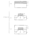
- Fig. 8 is a schematic cross-sectional view showing another example of the conventional ferroelectric memory having the MFMIS structure.
- the ferroelectric memory shown in Fig. 8 is disclosed in JP-A-5-327062.
- a source region 34 composed of a p + layer and a drain region 35 composed of a p + layer are formed with predetermined spacing on the surface of an n + silicon substrate 31.
- a region of the silicon substrate 31 between the source region 34 and the drain region 35 is a channel region 36.
- a gate oxide film 32 is formed on the channel region 36, and a first lower electrode 33 is formed on the gate oxide film 32.
- An interlayer insulating film 37 is formed on the silicon substrate 31 and the first lower electrode 33.
- a contact hole 39 is formed in the interlayer insulating film 37 on the first lower electrode 33, and a wiring layer 40 is formed in the contact hole 39.
- Contact holes are respectively provided in the interlayer insulating film 37 on the source region 34 and the interlayer insulating film 37 on the drain region 35, and wiring layers 45 and 46 are respectively formed in the contact holes.
- a second lower electrode 42 is formed on the wiring layer 40 connected to the first lower electrode 33.
- a ferroelectric thin film 43 is formed on the second lower electrode 42, and an upper electrode 44 is formed on the ferroelectric thin film 43.
- ohmic electrodes 47 and 48 are respectively formed on the wiring layers 45 and 46 which are connected to the source region 34 and the drain region 35.
- the ferroelectric thin film 43 is formed on the second lower electrode 42 composed of a material which is low in reactivity, for example, Pt, and the interlayer insulating film 37 is provided between the first lower electrode 33 and the second lower electrode 42, so that constituent atoms are further prevented from reacting with each other and mutually diffusing between the ferroelectric thin film 43 and the silicon substrate 31.
- a conductive material such as Pt which is a material for the upper electrode 44 and the second lower electrode 42 which have been etched may, in some cases, adhere or deposit on sidewalls of the ferroelectric thin film 43. Therefore, a current leaks between the upper electrode 44 and the second lower electrode 42, so that the reliability of the ferroelectric memory is decreased, and the fabrication yield thereof is decreased.
- An object of the present invention is to provide a dielectric device whose reliability and yield are prevented from being decreased by the adhesion or the deposition of a conductive material on sidewalls of a dielectric film.
- Another object of the present invention is to provide a dielectric memory whose reliability and yield are prevented from being decreased by the adhesion or the deposition of a conductive material on sidewalls of a dielectric film.
- Still another object of the present invention is to provide a method of fabricating a dielectric device whose reliability and yield are prevented from being decreased by the adhesion or the deposition of a conductive material on sidewalls of a dielectric film.
- a further object of the present invention is to provide a method of fabricating a dielectric memory whose reliability and yield are prevented from being decreased by the adhesion or the deposition of a conductive material on sidewalls of the dielectric film.
- a dielectric device comprises a first conductive layer, an insulating layer formed so as to cover the first conductive layer and having a contact hole, a second conductive layer provided in the contact hole of the insulating layer, and a dielectric film formed on the second conductive layer.
- the second conductive layer which is brought into contact with the dielectric film is provided in the contact hole of the insulating layer.
- a material for the second conductive layer does not adhere or deposit on sidewalls of the dielectric film. Consequently, the reliability and the yield are prevented from being decreased by the adhesion or the deposition of a conductive material on the sidewalls of the dielectric film.
- the dielectric film may be a ferroelectric film. In this case, the reliability and the yield of the dielectric device including the ferroelectric film are improved.
- the dielectric device may further comprise a third conductive layer formed on the dielectric film.
- a dielectric capacitor is constructed. Also in this case, since the second conductive layer which is contact with the dielectric film is provided in the contact hole of the insulating layer, reduction of the area of the capacitor is realized.
- the dielectric device may further comprise a connecting layer formed under the second conductive layer in the contact hole for electrically connecting the second conductive layer to the first conductive layer.
- the connecting layer and the second electrode layer are provided in the contact hole of the insulating layer, and the second conductive layer in the contact hole is electrically connected to the first conductive layer by the connecting layer.
- a dielectric memory provided in a semiconductor according to another aspect of the present invention comprises first and second impurity regions formed with predetermined spacing in the semiconductor, a gate insulating film formed on a region between the first and second impurity regions, a first lower electrode layer formed on the gate insulating film, an interlayer insulating film formed on the semiconductor so as to cover the first lower electrode layer and the gate insulating film and having a contact hole, a second lower electrode layer formed in the contact hole of the interlayer insulating film and electrically connected to the first lower electrode layer, a dielectric film formed on the interlayer insulating film so as to be brought into contact with the upper surface of the second lower electrode layer, and an upper electrode layer formed on the dielectric film.
- the second lower electrode layer which is brought into contact with the lower surface of the dielectric film is provided in the contact hole of the interlayer insulating film.
- a material for the second lower electrode layer does not adhere or deposit on sidewalls of the dielectric film.
- a current does not leak between the upper electrode layer and the second lower electrode layer because the second lower electrode layer is provided in the contact hole of the interlayer insulating film. Consequently, the reliability and the yield are prevented from being decreased by the adhesion or the deposition of a conductive material on the sidewalls of the dielectric film.
- the dielectric memory may further comprise a connecting layer formed under the second lower electrode layer in the contact hole for electrically connecting the second lower electrode layer to the first lower electrode layer.
- the connecting layer and the second lower electrode layer are provided in the contact hole of the interlayer insulating film, and the second lower electrode layer in the contact hole is electrically connected to the first lower electrode layer by the connecting layer.
- the dielectric memory may further comprise a buffer layer formed on the interlayer insulating film.
- the dielectric film is formed on the interlayer insulating film through the buffer layer, so that the stress applied to the dielectric film formed on the interlayer insulating film is retrieved. Therefore, the dielectric film is prevented from being cracked, and constituent elements are prevented from reacting with each other and mutually diffusing between the dielectric film and the interlayer insulating film.
- the dielectric film may be a ferroelectric film. In this case, the reliability and the yield of the dielectric memory including the ferroelectric film are improved.
- the ferroelectric film may have a perovskite crystal structure.
- the semiconductor may be a semiconductor substrate, or a semiconductor layer.
- the semiconductor may be silicon of a first conductivity type, and the first and second impurity regions may be formed of silicon of a second conductivity type opposite to the first conductivity type.
- a dielectric device comprises an insulating layer having a contact hole, a conductive layer provided in the contact hole of the insulating layer, and a dielectric film formed on the conductive layer.
- the conductive layer which is brought into contact with the dielectric film is provided in the contact hole of the insulating layer, so that a material for the conductive layer does not adhere or deposit on sidewalls of the dielectric film at the time of patterning the dielectric film. Consequently, the reliability and the yield are prevented from being decreased by the adhesion or the deposition of a conductive material on the sidewalls of the dielectric film.
- the dielectric device may further comprise another conductive layer formed on the dielectric film.
- a dielectric capacitor is constructed.
- a method of fabricating a dielectric device comprises the steps of forming a first conductive layer, forming an insulating layer on the first conductive layer, forming a contact hole in the insulating layer, forming a second conductive layer in the contact hole of the insulating layer, forming a dielectric film on the second conductive layer, and patterning the dielectric film.
- the second conductive layer is formed in the contact hole of the insulating layer.
- a material for the second conductive layer does not adhere or deposit on sidewalls of the dielectric film. Consequently, the reliability and the yield of the dielectric device are improved.
- the dielectric film may be a ferroelectric film. In this case, the reliability and the yield of the dielectric device including the ferroelectric film are improved.
- the fabricating method may further comprise the steps of forming a third conductive layer on the dielectric film, and patterning the third conductive layer. In this case, a dielectric capacitor is constructed.
- a method of fabricating a dielectric memory comprises the steps of forming a gate insulating layer on a channel region, forming a first lower electrode layer on the gate insulating film, forming an interlayer insulating film so as to cover the first lower electrode layer and the gate insulating film, forming a contact hole in the interlayer insulating film, forming a second lower electrode layer electrically connected to the first lower electrode layer in the contact hole of the interlayer insulating film, forming a dielectric film on the interlayer insulating film so as to be brought into contact with the upper surface of the second lower electrode layer, forming an upper electrode layer on the dielectric film, and patterning the upper electrode layer and the dielectric film.
- the second lower electrode layer is formed in the contact hole of the interlayer insulating film.
- a material for the second lower electrode layer does not adhere or deposit on sidewalls of the dielectric film. Even if a material for the upper electrode layer adheres or deposits on the sidewalls of the dielectric film, a current does not leak between the upper electrode layer and the second lower electrode layer because the second lower electrode layer is provided in the contact hole of the interlayer insulating film. Consequently, the reliability and the yield of the dielectric memory are improved.
- the step of forming the second lower electrode layer may comprise the steps of forming a connecting layer up to a predetermined depth in the contact hole, and forming an electrode layer on the connecting layer in the contact hole.
- the connecting layer and the second lower electrode layer are provided in the contact hole, and the second lower electrode layer is electrically connected to the first lower electrode layer by the connecting layer.
- the fabricating method may further comprise the step of forming a diffusion barrier layer on the connecting layer. Therefore, the oxidation of the connecting layer and the diffusion of impurities into the first lower electrode layer are prevented.
- the fabricating method may further comprise the step of forming a buffer layer on the interlayer insulating film.
- the dielectric film is formed on the interlayer insulating film through the buffer layer, so that the stress applied to the dielectric film is retrieved. Therefore, the dielectric film is prevented from being cracked, and constituent elements are prevented from reacting with each other and mutually diffusing between the dielectric film and the interlayer insulating film.
- the dielectric film may be a ferroelectric film. In this case, the reliability and the yield of the dielectric memory including the ferroelectric film are improved.
- the ferroelectric film may have a perovskite crystal structure.
- the fabricating method may further comprise the step of forming first and second impurity regions on both side of a channel region.
- the channel region may be formed of silicon of a first conductivity type
- the first and second impurity regions may be formed of silicon of a second conductivity type opposite to the first conductivity type.
- Fig. 1 is a schematic cross-sectional view showing the construction of a ferroelectric memory according to one embodiment of the present invention.
- a source region 4 composed of an n + layer and a drain region 5 composed of an n + layer are formed with predetermined spacing in the surface of a p-type single crystalline silicon substrate 1.
- a region of the silicon substrate 1 between the source region 4 and the drain region 5 is a channel region 6.
- a gate insulating film 2 composed of SiO 2 is formed on the channel region 6.
- a first lower electrode (a gate electrode) 3 composed of polysilicon is formed on the gate insulating film 2.
- An interlayer insulating film 7 is formed on the silicon substrate 1 so as to cover the first lower electrode 3 and the gate insulating film 2.
- a buffer layer 8 composed of TiO 2 (titanium oxide), CeO 2 (cerium oxide), etc. is formed on the interlayer insulating film 7.
- a contact hole 9 is formed in the interlayer insulating film 7 and the buffer layer 8 on the first lower electrode 3.
- a connecting layer (a plug) 10 composed of a conductive material such as polysilicon or W (tungsten) is formed up to a predetermined depth in the contact hole 9.
- a second lower electrode 12 composed of a conductive material such as Pt (platinum) or IrO 2 (iridium oxide) is formed on the connecting layer 10 in the contact hole 9.
- a ferroelectric thin film 13 composed of PZT (lead titanate zirconate) or SrBiTaO having a perovskite crystal structure is formed on the buffer layer 8 so as to be brought into contact with the upper surface of a second lower electrode 12.
- An upper electrode 14 composed of a conductive material such as Pt or IrO 2 is formed on the ferroelectric thin film 13.
- Contact holes are respectively formed in the buffer layer 8 and the interlayer insulating film 7 on the source region 4 and the buffer layer 8 and the interlayer insulating film 7 on the drain region 5, and a source electrode 15 and a drain electrode 16 which are composed of a conductive material such as polysilicon are respectively formed in the contact holes.
- Wiring layers 17 and 18 are respectively formed on the source electrode 15 and the drain electrode 16.
- the source region 4 and the drain region 5 respectively correspond to first and second impurity regions
- the first lower electrode 3 corresponds to a first conductive layer or a first lower electrode layer
- the second lower electrode 12 corresponds to a second lower electrode layer
- the connecting layer 10 corresponds to a connecting layer
- the connecting layer 10 and the second lower electrode 12 constitute a second conductive layer
- the upper electrode 14 corresponds to an upper electrode layer.
- Figs. 2, 3, 4 and 5 are cross-sectional views showing the steps of a method of fabricating the ferroelectric memory shown in Fig. 1.
- a gate insulating film 2 composed of SiO 2 having a thickness of 100 ⁇ is formed on a p-type silicon substrate 1 by a thermal oxidation method, and a first lower electrode 3 composed of polysilicon having a thickness of 2000 ⁇ is formed on the gate insulating film 2 by a CVD method (a chemical vapor deposition method).
- the first lower electrode 3 and the gate insulating film 2 in a portion excluding a gate forming region on the silicon substrate 1 are then removed using a dry process such as reactive-ion etching (RIE) or ion milling, to form a gate portion.
- RIE reactive-ion etching
- n-type impurities an n-type dopant
- a region of the silicon substrate 1 between the source region 4 and the drain region 5 is a channel region 6.
- an interlayer insulating film 7 composed of SiO 2 , etc. having a thickness of approximately 6000 ⁇ is formed by a CVD method or the like on the silicon substrate 1 so as to cover the first lower electrode 3 and the gate insulating film 2, as shown in Fig. 2 (c).
- a buffer layer 8 having a thickness of 500 ⁇ composed of TiO 2 , CeO 2 , etc. is then formed on the interlayer insulating film 7. Thereafter, a contact hole 9 is provided by a lithographic technique in the buffer layer 8 and the interlayer insulating film 7 on the first lower electrode 3, as shown in Fig. 3 (e).
- a connecting layer 10 composed of a conductive material such as polysilicon or W is formed in the contact hole 9.
- the thickness of the connecting layer 10 is set such that the distance from an upper end of the contact hole 9 to the upper surface of the connecting layer 10 is 1500 ⁇ .
- a conductive layer is formed on the inside of the contact hole 9 and the whole surface of the buffer layer 8, after which the whole surface is etched, to remove a conductive layer on the buffer layer 8.
- a diffusion barrier layer 11 composed of a conductive material such as TiN or TaSiN is then formed on the inside of the contact hole 9 and the whole surface of the buffer layser 8 by a sputtering method, a CVD method or the like in order to prevent the connecting layer 10 from being oxidized and prevent impurities from being diffused into a gate portion.
- the whole surface of the diffusion barrier layer 11 is etched, to remove the diffusion barrier layer 11 on the buffer layer 8 as well as to etch the buffer layer 11 back until the upper surface of the diffusion barrier layer 11 in the contact hole 9 is lower than the upper surface of the buffer layer 8.
- mixed gas of BCl 3 and Cl 2 is used as etching gas, and the etching conditions are an RF power of 250 W and a pressure of 2 ⁇ 10 -2 torr.
- the other gas such as Ar or N 2 may be mixed with the mixed gas.
- a diffusion barrier layer 11 having a thickness of 300 ⁇ is thus formed on the connecting layer 10 in the contact hole 9.
- the diffusion barrier layer 11 will be a part of the second lower electrode 12 formed in the subsequent process.
- a second lower electrode 12 having a thickness of 3000 ⁇ composed of a conductive material such as Pt or IrO 2 is then formed on the buffer layer 8 and the diffusion barrier layer 11 in the contact hole 9 by a sputtering method, a CVD method, a sol-gel method or the like.
- a sputtering method a sputtering method, a CVD method, a sol-gel method or the like.
- Another material on which a ferroelectric crystal can be grown may be used as a material for the second lower electrode 12.
- RuO x ruthenium oxide
- the second lower electrode 12 is then flattened by etch-back, a CMP method (a chemical mechanical polishing method) or the like, leaving the second lower electrode 12 in the contact hole 9, to form the second lower electrode 12 having a thickness of 1200 ⁇ in the contact hole 9.
- Cl 2 is used as etching gas
- the etching conditions are an RF power of 300 W and a pressure of 3 ⁇ 10 -3 torr.
- the etching gas the other gas such as Ar, HBr or BCl 3 may be used, or their mixed gas may be used.
- the second lower electrode 12 and the diffusion barrier layer 11 may be simultaneously flattened by etch-back or a CMP method after continuously forming the diffusion barrier layer 11 and the second lower electrode 12 instead of etching the diffusion barrier layer 11 back in the step shown in Fig. 4 (f).
- a ferroelectric thin film 13 having a thickness of 2000 ⁇ composed of PZT, SrBiTaO, etc. is then formed by a sol-gel method, a sputtering method, a CVD method or the like on the second lower electrode 12 and the buffer layer 8.
- an upper electrode 14 composed of a conductive material such as Pt or IrO 2 having a thickness of 1500 ⁇ is then formed by a sputtering method on the ferroelectric thin film 13.
- the upper electrode 14 and the ferroelectric thin film 13 are simultaneously patterned by etching, as shown in Fig. 6 (m).
- Cl 2 is used as etching gas
- the etching conditions are an RF power of 300 W and a pressure of 3 ⁇ 10 -3 torr.
- the etching gas the other gas such as Ar, CF 4 , SF 6 , HBr, or BCl 3 may be used, or their mixed gas may be used.
- the upper electrode 14 and the ferroelectric thin film 13 may be separately etched. At the time of etching, the whole of the buffer layer 8 may be etched.
- the ferroelectric thin film 13 need not necessarily extend over the buffer layer 8, provided that it is brought into contact with the upper surface of the second lower electrode 12.
- the buffer layer 8 and the interlayer insulating film 7 on the source electrode 4 and the buffer layer 8 and the interlayer insulating film 7 on the drain electrode 5 are then respectively provided with the contact holes, and a source electrode 15 and a drain electrode 16 composed of a conductive material such as polysilicon or tungsten are respectively formed in the contact holes, as shown in Fig. 1. Finally, wiring layers 17 and 18 composed of Al are respectively formed on the source electrode 15 and the drain electrode 16. A ferroelectric memory according to the present embodiment is thus fabricated.
- the second lower electrode 12 is provided in the contact hole 9 of the interlayer insulating film 7.
- the conductive material for the second lower electrode 12 does not adhere or deposit on sidewalls of the ferroelectric thin film 13. Even if the conductive material for the upper electrode 14 adheres or deposits on the sidewalls of the ferroelectric thin film 13, a current does not leak between the upper electrode 14 and the second lower electrode 12 because the second lower electrode 12 is provided in the contact hole 9 of the interlayer insulating film 7. As a result, the reliability and the yield of the ferroelectric memory are improved.
- the ferroelectric thin film 13 is formed on the interlayer insulating film 7 through the buffer layer 8, so that the stress applied to the ferroelectric thin film 13 is retrieved by the buffer layer 8. Therefore, the ferroelectric thin film 13 is prevented from being cracked, and constituent elements are prevented from reacting with each other (for example, reaction between Pb and SiO 2 ) and mutually diffusing between the ferroelectric thin film 13 and the interlayer insulating film 7. As a result, the reliability and the yield of the ferroelectric memory are further improved.
- the ferroelectric thin film 13 is formed on the second upper electrode 12 composed of a material which is low in reactivity, for example, Pt, and the interlayer insulating film 7 is provided between the ferroelectric thin film 13 and the silicon substrate 1, so that the constituent elements are sufficiently prevented from reacting with each other or mutually diffusing between the ferroelectric thin film 13 and the silicon substrate 1.
- the surface of the second lower electrode 12 with the ferroelectric thin film 13 is negatively charged, and the surface of the first lower electrode 3 with the gate insulating film 2 is positively charged.
- an inversion layer is formed in the channel region 6 between the source region 4 and the drain region 5, so that an FET is turned on, although the voltage of the upper electrode 14 is zero.
- the surface of the second lower electrode 12 with the ferroelectric thin film 13 is positively charged, and the surface of the first lower electrode 3 with the gate insulating film 2 is negatively charged.
- no inversion layer is formed in the channel region 6 between the source region 4 and the drain region 5, so that the FET is turned off.
- the FET When the ferroelectric thin film 13 is thus sufficiently polarized inversely, the FET can be selectively turned on or off even after a voltage applied to the upper electrode 14 is set to zero. Therefore, it is possible to discriminate between data "1" and "0" which are stored in the ferroelectric memory by detecting a current between a source and a drain.
- a voltage other than "0" by which the FET can be selectively turn on or off, may be applied to the upper electrode 14.
- ferroelectric thin film 13 ferroelectrics composed of the following materials may be used.
- a molecular beam epitaxy (MBE) method As a method of forming the ferroelectric thin film 13, a molecular beam epitaxy (MBE) method, a laser ablation method, a laser molecular beam epitaxy method, a sputtering method (of an RF (Radio Frequency) type, a DC (Direct Current) type, or an ion beam type), a reactive evaporation method, an MOCVD method (a metal organic chemical vapor deposition method), a mist deposition method, a sol-gel method, etc. can be used depending on the above-mentioned material for the ferroelectric thin film 13.
- MBE molecular beam epitaxy
- a material for the second lower electrode 12 and the upper electrode 14 are not limited to Pt or IrO 2 .
- the other material may be used. Examples include noble metals (Au, Ag, Pt, Ru, Rh, Pb, Os, Ir, etc.), high-melting point metals (Co, W, Ti, etc.), high-melting point metal compounds (TiN, IrSiN, etc.), conductive oxides (RuO 2 , RhO 2 , OsO 2 , IrO 2 , ReO 2 , ReO 3 , MoO 2 , WO 2 , SrRuO 3 , Pb 2 RuO 3-X , Bi 2 Ru 2 O 7-X , etc.), or alloys of the materials.
- the second lower electrode 12 and the upper electrode 14 may have a multilayer structure of the above-mentioned materials, or a two-layer structure in which a Pt layer is formed on a Ti layer, for example.
- Materials for the first lower electrode 3 and the connecting layer 10 are not limited to polysilicon or W. Other conductive materials may be used.
- the FET is formed on the silicon substrate 1, the FET may be formed on the other semiconductor substrate or semiconductor layer.
- ferroelectric memory having an n-type channel Although description was made of the ferroelectric memory having an n-type channel, a ferroelectric memory having a p-type channel is also realized by reversing the conductivity type of each layer.
- one contact hole 9 is provided in the interlayer insulating film 7 on the first lower electrode 3
- a plurality of contact holes may be formed in the interlayer insulating film 7 on the first lower electrode 3 so that second lower electrodes in the contact holes are brought into contact with the ferroelectric thin film 13.
- one ferroelectric thin film may be shared by a plurality of FETs so that the ferroelectric thin film is brought into contact with second lower electrodes in a plurality of contact holes provided in upper parts of the plurality of FETs.
- the present invention is also applicable to a ferroelectric memory which performs nonvolatile operations. Further, the present invention is also applicable to another dielectric device such as a capacitor having a structure in which a conductive layer is brought into contact with a dielectric film.
Abstract
Description
- Bi2O3 / SrTa2O6
- (SrBi2Ta2O9) : SBT
- Bi2O3 / SrNb2O6
- (SrBi2Nb2O9)
- Bi2O3 / SrTa2O6 / BaTiO3
- Bi2O3 / SrTaO6 / SrTiO3
- Bi2O3 / Bi2Ti3O9
- (Bi4Ti3O12) : BIT
- Bi2O3 / Sr3Ti4O12
- (Sr3Bi2Ti4O15)
- Bi2O3 / Bi2Ti3O9 / SrTiO3
- (SrBi4Ti4O15)
Claims (20)
- A dielectric device comprising:a first conductive layer;an insulating layer formed so as to cover said first conductive layer and having a contact hole;a second conductive layer provided in said contact hole of said insulating layer; anda dielectric film formed on said second conductive layer.
- The dielectric device according to claim 1, wherein
said dielectric film is a ferroelectric film. - The dielectric device according to claim 1, further comprising
a third conductive layer formed on said dielectric film. - The dielectric device according to claim 1, further comprising
a connecting layer formed under said second conductive layer in said contact hole for electrically connecting said second conductive layer to said first conductive layer. - A dielectric memory comprising:first and second impurity regions formed with predetermined spacing in a semiconductor;a gate insulating film formed on a region between said first and second impurity regions;a first lower electrode layer formed on said gate insulating film;an interlayer insulating film formed on said semiconductor so as to cover said first lower electrode layer and said gate insulating film and having a contact hole;a second lower electrode layer formed in said contact hole of said interlayer insulating film and electrically connected to said first lower electrode layer;a dielectric film formed on said interlayer insulating film so as to be brought into contact with the upper surface of said second lower electrode layer; andan upper electrode layer formed on said dielectric film.
- The dielectric memory according to claim 5, further comprising
a connecting layer formed under said second lower electrode layer in said contact hole for electrically connecting said second lower electrode layer to said first lower electrode layer. - The dielectric memory according to claim 5, further comprising
a buffer layer formed on said interlayer insulating film. - The dielectric memory according to claim 5, wherein
said dielectric film is a ferroelectric film. - The dielectric memory according to claim 8, wherein
said ferroelectric film has a perovskite crystal structure. - A dielectric device comprising:an insulating layer having a contact hole;a conductive layer provided in said contact hole of said insulating layer; anda dielectric film formed on said conductive layer.
- The dielectric device according to claim 10, further comprising
another conductive layer formed on said dielectric film. - A method of fabricating a dielectric device, comprising the steps of:forming a first conductive layer;forming an insulating layer on said first conductive layer;forming a contact hole in said insulating layer;forming a second conductive layer in said contact hole of said insulating layer;forming a dielectric film on said second conductive layer; andpatterning said dielectric film.
- The method according to claim 12, wherein
said dielectric film is a ferroelectric film. - The method according to claim 12, further comprising the steps offorming a third conductive layer on said dielectric film, andpatterning said third conductive layer.
- A method of fabricating a dielectric memory, comprising the steps of:forming a gate insulating film on a channel region;forming a first lower electrode layer on said gate insulating film;forming an interlayer insulating film so as to cover said first lower electrode layer and said gate insulating film;forming a contact hole in said interlayer insulating film;forming a second lower electrode layer electrically connected to said first lower electrode layer in said contact hole of said interlayer insulating film;forming a dielectric film on said interlayer insulating film so as to be brought into contact with the upper surface of said second lower electrode layer;forming an upper electrode layer on said dielectric film; andpatterning said upper electrode layer and said dielectric film.
- The method according to claim 15, whereinthe step of forming said second lower electrode layer comprises the steps offorming a connecting layer up to a predetermined depth of said contact hole, andforming an electrode layer on said connecting layer in said contact hole.
- The method according to claim 16, further comprising the step of
forming a diffusion barrier layer on said connecting layer. - The method according to claim 15, further comprising
forming a buffer layer on said interlayer insulating film. - The method according to claim 15, wherein
said dielectric film is a ferroelectric film. - The method according to claim 19, wherein
said ferroelectric film has a perovskite crystal structure.
Applications Claiming Priority (2)
| Application Number | Priority Date | Filing Date | Title |
|---|---|---|---|
| JP158809/97 | 1997-06-16 | ||
| JP15880997A JP3281839B2 (en) | 1997-06-16 | 1997-06-16 | Dielectric memory and method of manufacturing the same |
Publications (2)
| Publication Number | Publication Date |
|---|---|
| EP0886317A2 true EP0886317A2 (en) | 1998-12-23 |
| EP0886317A3 EP0886317A3 (en) | 1999-02-17 |
Family
ID=15679840
Family Applications (1)
| Application Number | Title | Priority Date | Filing Date |
|---|---|---|---|
| EP98304720A Ceased EP0886317A3 (en) | 1997-06-16 | 1998-06-15 | Dielectric device, Dielectric memory and method of fabricating the same |
Country Status (3)
| Country | Link |
|---|---|
| US (1) | US6194752B1 (en) |
| EP (1) | EP0886317A3 (en) |
| JP (1) | JP3281839B2 (en) |
Cited By (8)
| Publication number | Priority date | Publication date | Assignee | Title |
|---|---|---|---|---|
| EP0923117A1 (en) * | 1997-12-04 | 1999-06-16 | Sharp Kabushiki Kaisha | Method of manufacture of single transistor ferroelectric memory cell using chemical-mechanical polishing |
| EP1006590A1 (en) * | 1998-12-01 | 2000-06-07 | Rohm Co., Ltd. | Ferroelectric memory and method for manufacturing same |
| WO2000049660A1 (en) * | 1999-02-16 | 2000-08-24 | Symetrix Corporation | Iridium oxide diffusion barrier between local interconnect layer and thin film of layered superlattice material |
| EP1102329A2 (en) * | 1999-11-17 | 2001-05-23 | Sanyo Electric Co., Ltd. | Dielectric element |
| DE10009762A1 (en) * | 2000-03-01 | 2001-09-20 | Infineon Technologies Ag | Production of storage capacitor comprises applying cerium oxide layer to first electrode layer, applying amorphous dielectric layer, heating and applying second electrode layer on dielectric layer |
| US6762476B2 (en) | 2001-02-06 | 2004-07-13 | Sanyo Electric Co., Ltd | Dielectric element including oxide dielectric film and method of manufacturing the same |
| US6888189B2 (en) | 2000-11-08 | 2005-05-03 | Sanyo Electric Co., Ltd. | Dielectric element including oxide-based dielectric film and method of fabricating the same |
| EP1657738A2 (en) | 1999-02-04 | 2006-05-17 | Rohm Co., Ltd. | Capacitor and method for manufacturing the same |
Families Citing this family (16)
| Publication number | Priority date | Publication date | Assignee | Title |
|---|---|---|---|---|
| JP3171170B2 (en) * | 1998-05-25 | 2001-05-28 | 日本電気株式会社 | Thin film capacitor and method of manufacturing the same |
| JP2000349249A (en) * | 1999-06-08 | 2000-12-15 | Oki Electric Ind Co Ltd | Manufacture of semiconductor storage device |
| US6495878B1 (en) * | 1999-08-02 | 2002-12-17 | Symetrix Corporation | Interlayer oxide containing thin films for high dielectric constant application |
| EP1096502B1 (en) * | 1999-10-13 | 2005-06-29 | Rohm Co., Ltd. | Nonvolatile memory and its driving method |
| KR100612561B1 (en) * | 2000-06-19 | 2006-08-11 | 주식회사 하이닉스반도체 | Method of manufacturing a capacitor in a semiconductor device |
| US20020109166A1 (en) * | 2001-02-13 | 2002-08-15 | Hsu Sheng Teng | MFMOS/MFMS non-volatile memory transistors and method of making same |
| US6531324B2 (en) * | 2001-03-28 | 2003-03-11 | Sharp Laboratories Of America, Inc. | MFOS memory transistor & method of fabricating same |
| US6566148B2 (en) * | 2001-08-13 | 2003-05-20 | Sharp Laboratories Of America, Inc. | Method of making a ferroelectric memory transistor |
| DE10212962B4 (en) * | 2002-03-22 | 2007-11-29 | Qimonda Ag | Semiconductor memory cell with access transistor based on an organic semiconductor material and semiconductor memory device |
| US6531325B1 (en) * | 2002-06-04 | 2003-03-11 | Sharp Laboratories Of America, Inc. | Memory transistor and method of fabricating same |
| DE10308970A1 (en) * | 2003-02-28 | 2004-09-09 | Infineon Technologies Ag | Semiconductor memory cell and method for its production |
| DE10333557B8 (en) * | 2003-07-23 | 2008-05-29 | Qimonda Ag | Method for producing a memory device, memory cell, memory device and method for operating the memory device |
| KR100543528B1 (en) * | 2003-08-26 | 2006-01-31 | 한국과학기술연구원 | Fabrication method of self-aligned ferroelectric gate transistor using a buffer layer of high etching selectivity |
| KR100823168B1 (en) * | 2007-01-08 | 2008-04-18 | 삼성전자주식회사 | Ferroelectric memory device and method for forming the same |
| US9773793B2 (en) * | 2009-10-09 | 2017-09-26 | Texas Instuments Incorporated | Transistor performance modification with stressor structures |
| US10937783B2 (en) | 2016-11-29 | 2021-03-02 | Taiwan Semiconductor Manufacturing Co., Ltd. | Semiconductor device and manufacturing method thereof |
Citations (3)
| Publication number | Priority date | Publication date | Assignee | Title |
|---|---|---|---|---|
| JPH05327062A (en) * | 1992-05-22 | 1993-12-10 | Sharp Corp | Ferroelectric storage element |
| EP0697720A1 (en) * | 1994-08-01 | 1996-02-21 | Texas Instruments Incorporated | A conductive amorphous-nitride barrier layer for high dielectric-constant material electrodes |
| JPH0888334A (en) * | 1994-09-20 | 1996-04-02 | Nec Corp | Semiconductor device and manufacture thereof |
Family Cites Families (1)
| Publication number | Priority date | Publication date | Assignee | Title |
|---|---|---|---|---|
| US5731608A (en) * | 1997-03-07 | 1998-03-24 | Sharp Microelectronics Technology, Inc. | One transistor ferroelectric memory cell and method of making the same |
-
1997
- 1997-06-16 JP JP15880997A patent/JP3281839B2/en not_active Expired - Fee Related
-
1998
- 1998-06-15 US US09/094,592 patent/US6194752B1/en not_active Expired - Fee Related
- 1998-06-15 EP EP98304720A patent/EP0886317A3/en not_active Ceased
Patent Citations (4)
| Publication number | Priority date | Publication date | Assignee | Title |
|---|---|---|---|---|
| JPH05327062A (en) * | 1992-05-22 | 1993-12-10 | Sharp Corp | Ferroelectric storage element |
| EP0697720A1 (en) * | 1994-08-01 | 1996-02-21 | Texas Instruments Incorporated | A conductive amorphous-nitride barrier layer for high dielectric-constant material electrodes |
| JPH0888334A (en) * | 1994-09-20 | 1996-04-02 | Nec Corp | Semiconductor device and manufacture thereof |
| US5652446A (en) * | 1994-09-20 | 1997-07-29 | Nec Corporation | Semiconductor memory device with improved capacitor |
Non-Patent Citations (2)
| Title |
|---|
| PATENT ABSTRACTS OF JAPAN vol. 018, no. 144 (E-1521), 10 March 1994 & JP 05 327062 A (SHARP CORP), 10 December 1993, * |
| PATENT ABSTRACTS OF JAPAN vol. 096, no. 008, 30 August 1996 & JP 08 088334 A (NEC CORP), 2 April 1996, * |
Cited By (14)
| Publication number | Priority date | Publication date | Assignee | Title |
|---|---|---|---|---|
| EP0923117A1 (en) * | 1997-12-04 | 1999-06-16 | Sharp Kabushiki Kaisha | Method of manufacture of single transistor ferroelectric memory cell using chemical-mechanical polishing |
| US6900486B1 (en) | 1998-12-01 | 2005-05-31 | Rohm Co., Ltd. | Ferroelectric memory and method for manufacturing same |
| EP1006590A1 (en) * | 1998-12-01 | 2000-06-07 | Rohm Co., Ltd. | Ferroelectric memory and method for manufacturing same |
| US6656747B2 (en) | 1998-12-01 | 2003-12-02 | Rohm Co., Ltd. | Ferroelectric memory and method for manufacturing same |
| EP1657738A3 (en) * | 1999-02-04 | 2006-08-30 | Rohm Co., Ltd. | Capacitor and method for manufacturing the same |
| EP1657738A2 (en) | 1999-02-04 | 2006-05-17 | Rohm Co., Ltd. | Capacitor and method for manufacturing the same |
| WO2000049660A1 (en) * | 1999-02-16 | 2000-08-24 | Symetrix Corporation | Iridium oxide diffusion barrier between local interconnect layer and thin film of layered superlattice material |
| EP1102329A2 (en) * | 1999-11-17 | 2001-05-23 | Sanyo Electric Co., Ltd. | Dielectric element |
| US6720096B1 (en) | 1999-11-17 | 2004-04-13 | Sanyo Electric Co., Ltd. | Dielectric element |
| EP1102329A3 (en) * | 1999-11-17 | 2003-09-24 | Sanyo Electric Co., Ltd. | Dielectric element |
| DE10009762B4 (en) * | 2000-03-01 | 2004-06-03 | Infineon Technologies Ag | Manufacturing process for a storage capacitor with a dielectric based on strontium bismuth tantalate |
| DE10009762A1 (en) * | 2000-03-01 | 2001-09-20 | Infineon Technologies Ag | Production of storage capacitor comprises applying cerium oxide layer to first electrode layer, applying amorphous dielectric layer, heating and applying second electrode layer on dielectric layer |
| US6888189B2 (en) | 2000-11-08 | 2005-05-03 | Sanyo Electric Co., Ltd. | Dielectric element including oxide-based dielectric film and method of fabricating the same |
| US6762476B2 (en) | 2001-02-06 | 2004-07-13 | Sanyo Electric Co., Ltd | Dielectric element including oxide dielectric film and method of manufacturing the same |
Also Published As
| Publication number | Publication date |
|---|---|
| US6194752B1 (en) | 2001-02-27 |
| EP0886317A3 (en) | 1999-02-17 |
| JP3281839B2 (en) | 2002-05-13 |
| JPH118356A (en) | 1999-01-12 |
Similar Documents
| Publication | Publication Date | Title |
|---|---|---|
| US6194752B1 (en) | Dielectric device, dielectric memory and method of fabricating the same | |
| US5638319A (en) | Non-volatile random access memory and fabrication method thereof | |
| US6974985B2 (en) | Capacitor and method for fabricating the same, and semiconductor device and method for fabricating the same | |
| CA2225681C (en) | Barrier layer for ferroelectric capacitor integrated on silicon | |
| US6534326B1 (en) | Method of minimizing leakage current and improving breakdown voltage of polycrystalline memory thin films | |
| US7297999B1 (en) | Semiconductor device with capacitors and its manufacture method | |
| US6858492B2 (en) | Method for fabricating a semiconductor memory device | |
| JPH10242426A (en) | Capacitor structure of semiconductor memory cell and its manufacture | |
| US6291292B1 (en) | Method for fabricating a semiconductor memory device | |
| JP2003068993A (en) | Semiconductor device and its manufacturing method | |
| JP2001127262A (en) | Ferroelectrics capacitor, manufacturing method therefor, and semiconductor device | |
| US20100252867A1 (en) | MFMS-FET, Ferroelectric Memory Device, And Methods Of Manufacturing The Same | |
| JP2003086771A (en) | Capacitive element, and semiconductor device and its manufacturing method | |
| US20080160642A1 (en) | Semiconductor device | |
| US7153706B2 (en) | Ferroelectric capacitor having a substantially planar dielectric layer and a method of manufacture therefor | |
| KR100209748B1 (en) | Capacitor fabrication method of semiconductor device | |
| KR0155866B1 (en) | Ferroelectric memory device and its manufacturing method | |
| JP4095582B2 (en) | Semiconductor device and manufacturing method thereof | |
| JPH1168057A (en) | Dielectric device | |
| US7527984B2 (en) | Semiconductor device | |
| US8318560B2 (en) | Methods of forming integrated circuit devices including a capacitor | |
| JP2000150813A (en) | Semiconductor device and its manufacture | |
| JP2000174228A (en) | Semiconductor integrated circuit and manufacture thereof | |
| JPH113976A (en) | Dielectric element, ferroelectric memory and its operation method | |
| JPH10341003A (en) | Dielectric element and its manufacture |
Legal Events
| Date | Code | Title | Description |
|---|---|---|---|
| PUAI | Public reference made under article 153(3) epc to a published international application that has entered the european phase |
Free format text: ORIGINAL CODE: 0009012 |
|
| AK | Designated contracting states |
Kind code of ref document: A2 Designated state(s): DE FR GB |
|
| AX | Request for extension of the european patent |
Free format text: AL;LT;LV;MK;RO;SI |
|
| PUAL | Search report despatched |
Free format text: ORIGINAL CODE: 0009013 |
|
| RIN1 | Information on inventor provided before grant (corrected) |
Inventor name: ISHIZUKA, YOSHIYUKI Inventor name: GUESHI, TATSURO Inventor name: GOTO, TAKASHI Inventor name: FURUKAWA, HIROAKI Inventor name: HARADA, MITSUAKI Inventor name: OGASAHARA, SATORU |
|
| AK | Designated contracting states |
Kind code of ref document: A3 Designated state(s): AT BE CH CY DE DK ES FI FR GB GR IE IT LI LU MC NL PT SE |
|
| AX | Request for extension of the european patent |
Free format text: AL;LT;LV;MK;RO;SI |
|
| RTI1 | Title (correction) | ||
| 17P | Request for examination filed |
Effective date: 19990607 |
|
| AKX | Designation fees paid |
Free format text: DE FR GB |
|
| 17Q | First examination report despatched |
Effective date: 19991103 |
|
| RIC1 | Information provided on ipc code assigned before grant |
Free format text: 7H 01L 27/115 A, 7H 01L 21/02 B |
|
| GRAG | Despatch of communication of intention to grant |
Free format text: ORIGINAL CODE: EPIDOS AGRA |
|
| RIC1 | Information provided on ipc code assigned before grant |
Free format text: 7H 01L 27/115 A, 7H 01L 21/8246 B, 7H 01L 21/02 B |
|
| RTI1 | Title (correction) |
Free format text: DIELECTRIC MEMORY AND METHOD OF FABRICATING THE SAME |
|
| STAA | Information on the status of an ep patent application or granted ep patent |
Free format text: STATUS: THE APPLICATION HAS BEEN REFUSED |
|
| 18R | Application refused |
Effective date: 20020721 |