EP0886207A2 - Detektion grösster Übereinstimmung zwischen Daten mit Hilfe von Assoziativspeichereinheiten mit verschachelten Daten - Google Patents
Detektion grösster Übereinstimmung zwischen Daten mit Hilfe von Assoziativspeichereinheiten mit verschachelten Daten Download PDFInfo
- Publication number
- EP0886207A2 EP0886207A2 EP98850105A EP98850105A EP0886207A2 EP 0886207 A2 EP0886207 A2 EP 0886207A2 EP 98850105 A EP98850105 A EP 98850105A EP 98850105 A EP98850105 A EP 98850105A EP 0886207 A2 EP0886207 A2 EP 0886207A2
- Authority
- EP
- European Patent Office
- Prior art keywords
- data
- bit
- associative memory
- memory units
- designated
- Prior art date
- Legal status (The legal status is an assumption and is not a legal conclusion. Google has not performed a legal analysis and makes no representation as to the accuracy of the status listed.)
- Granted
Links
Images

Classifications
-
- G—PHYSICS
- G06—COMPUTING OR CALCULATING; COUNTING
- G06F—ELECTRIC DIGITAL DATA PROCESSING
- G06F7/00—Methods or arrangements for processing data by operating upon the order or content of the data handled
- G06F7/02—Comparing digital values
Definitions
- the present invention relates to a longest coincidence data detection, and more particularly to an apparatus and method for detecting a longest coincidence data between an external data externally supplied and an internal data internally stored.
- a longest coincidence data detecting apparatus compares an internal data internally stored with an external data externally supplied to detect the longest coincidence data between the internal data and the external data.
- the longest coincidence data detecting apparatus is conventionally composed of a single associative memory unit or a plurality of associative memory units which are connected in series. The comparison is performed to detect the longest coincidence data while the mask bits for the associative memory units in the whole apparatus are shifted one bit by one bit.
- an associative memory apparatus which includes a data memory, a counter for counting an address of the data memory, and a mechanism for comparing a search data and an output of the data memory and for stopping the counter when the comparing result indicates matching.
- the associative memory apparatus is composed of a search data memory for storing a plurality of search data, a selecting means for selecting a specific one of the plurality of search data stored in the search data memory, the mechanism for comparing a portion of the selected search data in a specific comparison region and a portion of a data read out from the data memory corresponding to the comparison region for the selected search data, and for stopping the counter when the comparing result indicates coincidence, and another mechanism for restarting the counter from an address next to the stopped address.
- an object of the present invention is to provide an apparatus and method for detecting a longest coincidence data, in which a longest coincidence data can detected at high speed.
- each of the N associative memory units compares a distributed portion of the external data and a corresponding portion of an internal data in a designated bit region from a most significant bit of the distributed portion, and outputs a matching signal when the distributed portion of the external data portion and the corresponding portion of the internal data are coincident with each other in the designated bit region.
- the longest coincidence data detecting apparatus further includes a coincidence determination unit for generating a matching signal indicative of coincidence between the external data and the internal data in the designated bit region when the matching signals are received from the N associative memory units.
- the control section supplies to the N associative memory units, the mask bit data which indicates the designated bit region narrowed by one bit from a least significant bit of the distributed portion of the external data each time a shift signal is inputted.
- the mask bit data which indicates the designated bit region narrowed by one bit from a least significant bit of the distributed portion of the external data each time a shift signal is inputted.
- all bits of an initial data of the mask bit data are "1"
- each bit of the initial data of the mask bit data is changed to "0" from a least significant bit each time the shift signal is inputted, and the designated bit region is designated based on the bits of "1" of the mask bit data.
- the longest coincidence data detecting apparatus may further include a bit count outputting section for outputting a data indicative of a number of bits for which the external data and the internal data are not coincident with each other from a least significant bit of the external data, from a number of times of the input of the shift signal and the matching signals from the N associative memory units.
- the longest coincidence data detecting apparatus may further include a bit count outputting section for outputting a data indicative of a number of bits for which the external data and the internal data are not coincident with each other from a least significant bit of the external data, from the designated bit region.
- the bit count outputting section includes a counter for counting a number of times of input of a shift signal to produce a count data, the shift signal being used to determine the designated bit region, a flip-flop for outputting an output state data indicative of whether the matching signal is already outputted from the first associative memory unit, and a subtracting unit for subtracting the output state data from a data derived from the count data to output a matching bit count data indicative of the number of bits for which the external data and the internal data are coincident with each other from the least significant bit.
- a method of detecting a longest coincidence data comprises the steps of:
- a longest coincidence data detecting apparatus includes a plurality of associative memory units, each of which compares a portion of an external data and a corresponding portion of an internal data in accordance with a mask bit data, and outputs a matching signal when the external data portion and the corresponding portion of the internal data are coincident with each other in the region designated by the mask bit data, a control section for respectively supplying the portions of the external data to the plurality of associative memory units in response to a start signal, for shifting a designation data by one bit from a least significant bit to produce a shifted designation data each time a shift signal is inputted, and for outputting, as the mask bit data to all of the plurality of associative memory units, the designation data when no shift signal is inputted, and the shifted designation data when the shift signal is inputted, and a coincidence determination unit for generating a matching signal indicative of coincidence between the external data and the internal data in portion when the matching signals are received from the plurality of associative
- Fig. 1 is a circuit block diagram illustrating the structure of the longest coincidence data detecting apparatus according to an embodiment of the present invention. In this embodiment, two associative memory units are provided.
- the longest coincidence data detecting apparatus in the embodiment is composed of control circuits 1a and 1b, associative memory units (CAMs) 2a and 2b, an AND gate 3, a counter 4, a D-type flip-flop (DQ) 5, and a subtracting unit 6.
- the control circuits 1a and 1b receive two 8 bits of a 16-bit external data and the two 8 bits to the associative memory units 2a and 2b in response to a START signal, respectively. Also, the control circuits la and 1b each have mask bit data and shifts the mask bit data one bit by one bit from the least significant bit to the most significant bit in response to a SHIFT signal. The shifted mask bit data are supplied to the associative memory units 2a and 2b, respectively. In this manner, the same mask bit data is supplied to the associative memory units 2a and 2b.
- Each of the associative memory units 2a and 2b receives a portion of the external data outputted from a corresponding one of the control circuits 1a and 1b. Then, the associative memory unit compares the received portion of the external data and the portion of an internal data stored therein based on the mask bit data supplied from the control circuit. The associative memory unit 2a or 2b outputs a matching signal MATCH1 and MATCH0 when the received portion of the external data and the portion of the internal data are coincident with or match to each other.
- the AND gate 3 calculates a logic product of the matching signals outputted from the associative memory units 2a and 2b to output the calculation result as a MATCH signal. That is, the AND gate 3 outputs the MATCH signal indicating that the external data and the internal data are coincident within a region designated by the mask bit data.
- the counter 4 is reset in response to the START signal and counts the number of times of input of the SHIFT signal.
- the D-type flip-flop 5 is reset in response to the START signal.
- the D-type flip-flop 5 receives the SHIFT signal as a clock signal, and outputs the MATCH1 signal supplied from the associative memory unit 2a in response to the clock signal.
- the subtracting unit -6 subtracts the data which is outputted from the D-type flip-flop 5 from a data corresponding to the count value supplied from the counter 4 to output the subtracting result as a MASKBITS signal.
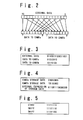
- Fig. 2 is a diagram illustrating the distribution of an external data to associative memory units in the longest coincidence data detecting apparatus according to the embodiment of the present invention.
- Fig. 3 is a diagram illustrating an example of the external data and distribution of the external data in the longest coincidence data detecting apparatus according to the embodiment of the present invention.
- Fig. 4 is a diagram illustrating an example of the internal data and the external expression of the internal data in the longest coincidence data detecting apparatus according to the embodiment of the present invention.
- Fig. 5 is a diagram illustrating the changing state of a mask bit data in the longest coincidence data detecting apparatus according to the embodiment of the present invention.
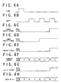
- Figs. 6A to 6H are timing charts to describe the operation of the longest coincidence data detecting apparatus according to the embodiment of the present invention.
- two 8-bit data of the 16-bit external data shown in Fig. 3 are supplied to the control circuits la and 1b, respectively.
- Y k is the k-th bit of the external data.
- X 0j is the j-th bit of the first 8-bit data which is inputted to the control circuit la
- X 1j is the j-th bit of the second 8-bit data which is inputted to the control circuit 1b.
- the two 8-bit data are supplied from the control circuits la and 1b to the associative memory units 2a and 2b in response to the START signal, respectively, as shown in Fig. 6A. Also, a mask bit data is set to "11111111" in response to the START signal, as shown in Fig. 5. Then, the same mask bit data is also supplied from the control circuits 1a and 1b to the associative memory units, respectively, in response to the START signal.
- the data bit of the mask bit data corresponding to "1" indicates that the comparison between the external data and the internal data should be performed in a bit position corresponding to the mask bit of "1".
- the data bit of the mask bit corresponding to "0" indicates that the comparison between the external data and the internal data should not be performed in a bit position corresponding to the mask bit of "0".
- the mask bit data of "11111111” means that all the bits of the 8-bit external data portion are compared with all the bits of the 8-bit internal data portion.
- the mask bit data of "11111110” means that all the bits of the 8-bit external data portion other than the least significant bit are compared with all the bits of the 8-bit internal data portion other than the least significant bit.
- the external expression of the internal data is "0110 0111 0000 0000" shown in Fig. 4.
- the external data and the stored data are not coincident with each other in the associative memory units 2a and 2b. Therefore, the matching signals MATCHO and MATCH1 are both "0". As a result of that, the MATCH signal which is the logic product of them also becomes "0".
- This mask bit data is supplied to the associative memory units 2a and 2b, and the comparison is performed so as to ignore the least significant bit.
- the counter 4 is counted up by "1” so that "1" is output from the counter 4, as shown in Fig. 6F.
- either of the MATCHO signal or the MATCH1 signal is “0” as shown in Figs. 6C and 6D and therefore the MATCH signal is still “0” as shown in Fig. 6E.
- the mask bit data for the associative memory units 2a and 2b are set to "11111100", as shown in Fig. 5.
- the comparison is performed while the lower 2 bits are ignored.
- the MATCH1 signal of "1" is outputted from the associative memory unit 2a.
- the MATCH0 signal of "0” is outputted from the associative memory unit 2b to the AND gate 3 and the D-type flip-flop 5, as shown in Fig. 6G.
- the counter 4 is counted up to output "2", as shown in Fig. 6F. In this case, because the MATCH0 signal is "0", the MATCH signal is also "0". However, the MATCH1 signal of "1” is supplied to the D-type flip-flop 5.
- the counter 4 is counted up by "1" to output "3", as shown in Fig. 6F.
- the MATCH0 signal is set to "1" as shown in Fig. 6C.
- the logical product of the MATCHO signal and the MATCH1 signal is set to "1" as the MATCH signal as shown in Fig. 6E.
- the output of the flip-flop 5 is set to "1" in response to the SHIFT signal, as shown in Fig. 6E.
- the output of "3" from the counter 4 is supplied to the subtracting unit 6.
- "0" is applied to the binary expression of the count value of the counter 4 as the least significant bit, i.e., "110” is obtained. Therefore, the subtracting unit 6 subtracts the data of "1” supplied from the D-type flip-flop 5 from the binary expression of "110". As a result of "101", that is "5" is obtained. This value is outputted as the MASKBITS signal.
- the output of the counter 4 is "3". Therefore, the least significant bit of "0" is added to the binary expression of the output of the counter 4, so that the output of the counter 4 is set to "6", i.e., "110".
- the MASKBITS signal is set to "5" as shown in Fig. 6H. This means that the lower 5 bits from the least significant bit must be ignored to make the external data and the external expression of the internal data portions to be coincident with each other.
- a circuit section composed of the counter 4, the flip-flop 5 and the subtracting unit 6 functions to detect the number of bits of the non-coincident portion between the external data and the internal data.
- the circuit section may output the number of bits of coincident portion between the external data and the internal data.
- an external data of L bits and an internal data of L bits are compared to detect the longest coincidence data between the external data and the internal data.
- a counter for counting a SHIFT signal externally inputted
- a flip-flop for outputting a signal outputted from associative memory means using the SHIFT signal as a clock signal
- a subtracting unit for subtracting and outputting a signal outputted from the flip-flop from the count value by the counter.
Landscapes
- Physics & Mathematics (AREA)
- General Physics & Mathematics (AREA)
- Engineering & Computer Science (AREA)
- Theoretical Computer Science (AREA)
- Computational Mathematics (AREA)
- Mathematical Analysis (AREA)
- Mathematical Optimization (AREA)
- Pure & Applied Mathematics (AREA)
- General Engineering & Computer Science (AREA)
- Information Retrieval, Db Structures And Fs Structures Therefor (AREA)
- Error Detection And Correction (AREA)
- Synchronisation In Digital Transmission Systems (AREA)
Applications Claiming Priority (3)
| Application Number | Priority Date | Filing Date | Title |
|---|---|---|---|
| JP162714/97 | 1997-06-19 | ||
| JP16271497 | 1997-06-19 | ||
| JP9162714A JP3036467B2 (ja) | 1997-06-19 | 1997-06-19 | 最長一致検出装置 |
Publications (3)
| Publication Number | Publication Date |
|---|---|
| EP0886207A2 true EP0886207A2 (de) | 1998-12-23 |
| EP0886207A3 EP0886207A3 (de) | 1999-12-08 |
| EP0886207B1 EP0886207B1 (de) | 2003-05-21 |
Family
ID=15759905
Family Applications (1)
| Application Number | Title | Priority Date | Filing Date |
|---|---|---|---|
| EP98850105A Expired - Lifetime EP0886207B1 (de) | 1997-06-19 | 1998-06-11 | Detektion grösster Übereinstimmung zwischen Daten mit Hilfe von Assoziativspeichereinheiten mit verschachelten Daten |
Country Status (5)
| Country | Link |
|---|---|
| US (1) | US6098147A (de) |
| EP (1) | EP0886207B1 (de) |
| JP (1) | JP3036467B2 (de) |
| AU (1) | AU736553B2 (de) |
| CA (1) | CA2239367C (de) |
Cited By (1)
| Publication number | Priority date | Publication date | Assignee | Title |
|---|---|---|---|---|
| EP1425755A4 (de) * | 2001-08-22 | 2005-11-09 | Netlogic Microsystems Inc | Gleichzeitiges durchsuchen verschiedener tabellen in einem inhaltsadressierbaren speicher |
Families Citing this family (22)
| Publication number | Priority date | Publication date | Assignee | Title |
|---|---|---|---|---|
| EP0936625A3 (de) * | 1998-02-17 | 2003-09-03 | Texas Instruments Incorporated | Assoziativspeicher (CAM) |
| US6757779B1 (en) | 1999-09-23 | 2004-06-29 | Netlogic Microsystems, Inc. | Content addressable memory with selectable mask write mode |
| US6801981B1 (en) | 2000-06-14 | 2004-10-05 | Netlogic Microsystems, Inc. | Intra-row configurability of content addressable memory |
| US6799243B1 (en) | 2000-06-14 | 2004-09-28 | Netlogic Microsystems, Inc. | Method and apparatus for detecting a match in an intra-row configurable cam system |
| US6813680B1 (en) | 2000-06-14 | 2004-11-02 | Netlogic Microsystems, Inc. | Method and apparatus for loading comparand data into a content addressable memory system |
| US6542391B2 (en) | 2000-06-08 | 2003-04-01 | Netlogic Microsystems, Inc. | Content addressable memory with configurable class-based storage partition |
| US6944709B2 (en) | 1999-09-23 | 2005-09-13 | Netlogic Microsystems, Inc. | Content addressable memory with block-programmable mask write mode, word width and priority |
| US6934795B2 (en) | 1999-09-23 | 2005-08-23 | Netlogic Microsystems, Inc. | Content addressable memory with programmable word width and programmable priority |
| US6751701B1 (en) | 2000-06-14 | 2004-06-15 | Netlogic Microsystems, Inc. | Method and apparatus for detecting a multiple match in an intra-row configurable CAM system |
| JP4298104B2 (ja) | 2000-01-18 | 2009-07-15 | Okiセミコンダクタ株式会社 | 連想メモリ |
| US6560670B1 (en) | 2000-06-14 | 2003-05-06 | Netlogic Microsystems, Inc. | Inter-row configurability of content addressable memory |
| SG118110A1 (en) * | 2001-02-01 | 2006-01-27 | Semiconductor Energy Lab | Organic light emitting element and display device using the element |
| US6910097B1 (en) | 2001-04-09 | 2005-06-21 | Netlogic Microsystems, Inc. | Classless interdomain routing using binary content addressable memory |
| US7210003B2 (en) | 2001-10-31 | 2007-04-24 | Netlogic Microsystems, Inc. | Comparand generation in a content addressable memory |
| US7237058B2 (en) | 2002-01-14 | 2007-06-26 | Netlogic Microsystems, Inc. | Input data selection for content addressable memory |
| US6934796B1 (en) | 2002-02-01 | 2005-08-23 | Netlogic Microsystems, Inc. | Content addressable memory with hashing function |
| US7382637B1 (en) | 2002-02-01 | 2008-06-03 | Netlogic Microsystems, Inc. | Block-writable content addressable memory device |
| US6697276B1 (en) | 2002-02-01 | 2004-02-24 | Netlogic Microsystems, Inc. | Content addressable memory device |
| US6700809B1 (en) | 2002-02-01 | 2004-03-02 | Netlogic Microsystems, Inc. | Entry relocation in a content addressable memory device |
| US7114026B1 (en) | 2002-06-17 | 2006-09-26 | Sandeep Khanna | CAM device having multiple index generators |
| US6842358B2 (en) * | 2002-08-01 | 2005-01-11 | Netlogic Microsystems, Inc. | Content addressable memory with cascaded array |
| US20060018142A1 (en) * | 2003-08-11 | 2006-01-26 | Varadarajan Srinivasan | Concurrent searching of different tables within a content addressable memory |
Family Cites Families (6)
| Publication number | Priority date | Publication date | Assignee | Title |
|---|---|---|---|---|
| DE2712575C2 (de) * | 1977-03-22 | 1985-12-19 | Walter Dipl.-Ing. 8011 Putzbrunn Motsch | Assoziatives Speichersystem in hochintegrierter Halbleitertechnik |
| JPH0632225B2 (ja) * | 1985-01-11 | 1994-04-27 | 株式会社日立製作所 | 連想メモリ装置 |
| US5113339A (en) * | 1987-10-20 | 1992-05-12 | Sharp Kabushiki Kaisha | Data processor for detecting identical data simultaneously coexisting in a plurality of data sections of data transmission paths |
| JPH0285927A (ja) * | 1988-09-22 | 1990-03-27 | Hitachi Vlsi Eng Corp | 記憶装置 |
| AU624205B2 (en) * | 1989-01-23 | 1992-06-04 | General Electric Capital Corporation | Variable length string matcher |
| JPH05233211A (ja) * | 1992-02-25 | 1993-09-10 | Seiko Epson Corp | 最長一致文字列検出回路 |
-
1997
- 1997-06-19 JP JP9162714A patent/JP3036467B2/ja not_active Expired - Fee Related
-
1998
- 1998-06-02 CA CA002239367A patent/CA2239367C/en not_active Expired - Fee Related
- 1998-06-11 EP EP98850105A patent/EP0886207B1/de not_active Expired - Lifetime
- 1998-06-16 US US09/097,598 patent/US6098147A/en not_active Expired - Fee Related
- 1998-06-18 AU AU71970/98A patent/AU736553B2/en not_active Ceased
Cited By (1)
| Publication number | Priority date | Publication date | Assignee | Title |
|---|---|---|---|---|
| EP1425755A4 (de) * | 2001-08-22 | 2005-11-09 | Netlogic Microsystems Inc | Gleichzeitiges durchsuchen verschiedener tabellen in einem inhaltsadressierbaren speicher |
Also Published As
| Publication number | Publication date |
|---|---|
| AU736553B2 (en) | 2001-08-02 |
| EP0886207B1 (de) | 2003-05-21 |
| CA2239367A1 (en) | 1998-12-19 |
| CA2239367C (en) | 2001-08-07 |
| AU7197098A (en) | 1998-12-24 |
| JPH117782A (ja) | 1999-01-12 |
| JP3036467B2 (ja) | 2000-04-24 |
| US6098147A (en) | 2000-08-01 |
| EP0886207A3 (de) | 1999-12-08 |
Similar Documents
| Publication | Publication Date | Title |
|---|---|---|
| EP0886207B1 (de) | Detektion grösster Übereinstimmung zwischen Daten mit Hilfe von Assoziativspeichereinheiten mit verschachelten Daten | |
| US4575818A (en) | Apparatus for in effect extending the width of an associative memory by serial matching of portions of the search pattern | |
| US7484063B2 (en) | Sorting method and apparatus using a CAM | |
| US4141268A (en) | Keyboard apparatus for an electronic musical instrument | |
| EP0481494B1 (de) | Speicheranordnung | |
| EP0234038A2 (de) | Vorrichtung zur Identifizierung der LRU-Speichereinheit in einem Speichersystem | |
| US5638017A (en) | Pulse width modulation circuit | |
| EP0568374B1 (de) | Parallelisierter Grössevergleicher zum Vergleichen einer Binärzahl mit einer bestimmten Zahl | |
| US5835428A (en) | Method of testing semiconductor memory and apparatus for carrying out the method | |
| US5488325A (en) | Timing generator intended for semiconductor testing apparatus | |
| US4592013A (en) | Method and device for addressing a memory | |
| KR920003176B1 (ko) | 정렬처리장치의 제어데이타 생성장치 | |
| US20040250013A1 (en) | Associative memory system, network device, and network system | |
| US5796918A (en) | Method for ranking membership function values of linguistic input values in a fuzzy logic processor and arrangement for the implementation thereof | |
| US6611894B1 (en) | Data retrieval apparatus | |
| US4586162A (en) | Bit pattern check circuit | |
| US6384713B1 (en) | Serial comparator | |
| US5379410A (en) | Data generating apparatus generating consecutive data and having a data skip scheme and a method of operating the same | |
| KR20000022936A (ko) | Fifo메모리장치 및 그 제어방법 | |
| US5260887A (en) | Bit data shift amount detector | |
| US6763422B2 (en) | Cache memory capable of reducing area occupied by data memory macro units | |
| US6311199B1 (en) | Sign extension unit | |
| EP1174790A1 (de) | Methode und Apparat zum Bestimmen der Anzahl von verfügbaren Speicherplätzen in einem FIFO-Speicher | |
| KR960002032A (ko) | 인터페이스 장치 | |
| US5977864A (en) | High speed comparator with bit-wise masking |
Legal Events
| Date | Code | Title | Description |
|---|---|---|---|
| PUAI | Public reference made under article 153(3) epc to a published international application that has entered the european phase |
Free format text: ORIGINAL CODE: 0009012 |
|
| 17P | Request for examination filed |
Effective date: 19980616 |
|
| AK | Designated contracting states |
Kind code of ref document: A2 Designated state(s): FI SE |
|
| AX | Request for extension of the european patent |
Free format text: AL;LT;LV;MK;RO;SI |
|
| PUAL | Search report despatched |
Free format text: ORIGINAL CODE: 0009013 |
|
| AK | Designated contracting states |
Kind code of ref document: A3 Designated state(s): AT BE CH CY DE DK ES FI FR GB GR IE IT LI LU MC NL PT SE |
|
| AX | Request for extension of the european patent |
Free format text: AL;LT;LV;MK;RO;SI |
|
| AKX | Designation fees paid |
Free format text: FI SE |
|
| REG | Reference to a national code |
Ref country code: DE Ref legal event code: 8566 |
|
| GRAG | Despatch of communication of intention to grant |
Free format text: ORIGINAL CODE: EPIDOS AGRA |
|
| 17Q | First examination report despatched |
Effective date: 20020507 |
|
| GRAG | Despatch of communication of intention to grant |
Free format text: ORIGINAL CODE: EPIDOS AGRA |
|
| GRAH | Despatch of communication of intention to grant a patent |
Free format text: ORIGINAL CODE: EPIDOS IGRA |
|
| GRAH | Despatch of communication of intention to grant a patent |
Free format text: ORIGINAL CODE: EPIDOS IGRA |
|
| GRAA | (expected) grant |
Free format text: ORIGINAL CODE: 0009210 |
|
| AK | Designated contracting states |
Designated state(s): FI SE |
|
| REG | Reference to a national code |
Ref country code: SE Ref legal event code: TRGR |
|
| PLBE | No opposition filed within time limit |
Free format text: ORIGINAL CODE: 0009261 |
|
| STAA | Information on the status of an ep patent application or granted ep patent |
Free format text: STATUS: NO OPPOSITION FILED WITHIN TIME LIMIT |
|
| 26N | No opposition filed |
Effective date: 20040224 |
|
| PGFP | Annual fee paid to national office [announced via postgrant information from national office to epo] |
Ref country code: SE Payment date: 20090605 Year of fee payment: 12 Ref country code: FI Payment date: 20090616 Year of fee payment: 12 |
|
| PG25 | Lapsed in a contracting state [announced via postgrant information from national office to epo] |
Ref country code: FI Free format text: LAPSE BECAUSE OF NON-PAYMENT OF DUE FEES Effective date: 20100611 |
|
| EUG | Se: european patent has lapsed | ||
| PG25 | Lapsed in a contracting state [announced via postgrant information from national office to epo] |
Ref country code: SE Free format text: LAPSE BECAUSE OF NON-PAYMENT OF DUE FEES Effective date: 20100612 |