EP0884802B1 - Terminal und Gehäuse mit Terminal - Google Patents
Terminal und Gehäuse mit Terminal Download PDFInfo
- Publication number
- EP0884802B1 EP0884802B1 EP98110174A EP98110174A EP0884802B1 EP 0884802 B1 EP0884802 B1 EP 0884802B1 EP 98110174 A EP98110174 A EP 98110174A EP 98110174 A EP98110174 A EP 98110174A EP 0884802 B1 EP0884802 B1 EP 0884802B1
- Authority
- EP
- European Patent Office
- Prior art keywords
- female terminal
- housing
- terminal
- section
- pair
- Prior art date
- Legal status (The legal status is an assumption and is not a legal conclusion. Google has not performed a legal analysis and makes no representation as to the accuracy of the status listed.)
- Expired - Lifetime
Links
Images


Classifications
-
- H—ELECTRICITY
- H01—ELECTRIC ELEMENTS
- H01R—ELECTRICALLY-CONDUCTIVE CONNECTIONS; STRUCTURAL ASSOCIATIONS OF A PLURALITY OF MUTUALLY-INSULATED ELECTRICAL CONNECTING ELEMENTS; COUPLING DEVICES; CURRENT COLLECTORS
- H01R13/00—Details of coupling devices of the kinds covered by groups H01R12/70 or H01R24/00 - H01R33/00
- H01R13/02—Contact members
- H01R13/10—Sockets for co-operation with pins or blades
- H01R13/11—Resilient sockets
- H01R13/112—Resilient sockets forked sockets having two legs
-
- H—ELECTRICITY
- H01—ELECTRIC ELEMENTS
- H01R—ELECTRICALLY-CONDUCTIVE CONNECTIONS; STRUCTURAL ASSOCIATIONS OF A PLURALITY OF MUTUALLY-INSULATED ELECTRICAL CONNECTING ELEMENTS; COUPLING DEVICES; CURRENT COLLECTORS
- H01R12/00—Structural associations of a plurality of mutually-insulated electrical connecting elements, specially adapted for printed circuits, e.g. printed circuit boards [PCB], flat or ribbon cables, or like generally planar structures, e.g. terminal strips, terminal blocks; Coupling devices specially adapted for printed circuits, flat or ribbon cables, or like generally planar structures; Terminals specially adapted for contact with, or insertion into, printed circuits, flat or ribbon cables, or like generally planar structures
- H01R12/70—Coupling devices
- H01R12/71—Coupling devices for rigid printing circuits or like structures
- H01R12/712—Coupling devices for rigid printing circuits or like structures co-operating with the surface of the printed circuit or with a coupling device exclusively provided on the surface of the printed circuit
- H01R12/716—Coupling device provided on the PCB
Definitions
- the present invention relates to An electrical connector for electrically, and mechanically connecting an electronic apparatus such as a hard disk drive to a printed circuit board.
- some of such miniaturized electrical connectors have female terminal, for electrically connecting to pin-like male terminals, being formed flat by a conductive plate member.
- the female terminals a pair of contacts portions opposed in a plane at a predetermined space are supported by a plate-like base portion through a pair of arm portions.
- the arm sections are pressed by means of the male terminal, and then, move along a surface of the plate member.
- the arm portions urges the paired contact portions toward a pin-like male terminal with a spring force generated by the movement of arm portions. Even if a thickness of the arm section is thin, a great spring force is created in the arm sections, so that the female terminal and the male terminal can be mechanically and electrically connected to each other.
- such a female terminal is disclosed in EP-A-0 777 306 comprising a pair of contact sections for contacting to a male terminal.
- US-A-4 781 612 an which the preamble of claim 1 is based, describes a female terminal for a card connector having a pair of contact sections and a base section wherefrom said pair of contact section extends in a way of being inclined with respect to the longitudinal axis of said female terminal.
- Said female terminal is supported by a lateral web engaging a housing projection for mounting said female terminal.
- Said terminal configuration requires much space based on its lateral dimension and it is, thus, disadvantageous for the miniaturization of connectors. Further, such a terminal is expensive in manufacture.
- a female terminal for an electrical connector comprising a pair of contact sections for projecting into an insertion slot of a housing; a base section supporting said contact sections via a pair of arm sections; said arm sections extending from said base section in a state of being inclined with respect to the axial line of said insertion slot, characterized by further comprising a middle tongue section extending from said base section between said pair of contact sections for inserting into a retaining slot of said housing being open along its axial line.
- a housing for an electrical connector made of an insulative material having a plurality of insertion slots for receiving male terminals each having a pair of opposed sides and an open end; a female terminal as described above, characterized by further comprising a retaining portion for retaining the base section of said female terminal; a slot for holding said middle tongue section of said female terminal having one open end in said recess portion and extending toward said open end of said insertion slot and being open along its axial line.
- the housing may have guide grooves which are individually formed on the mutually opposed side wall portions on both sides of the side wall portion formed with the recess portion of being the retaining portion so as to receive the arm sections.
- the arm sections of the female terminal slide in the guide grooves, so that a spring effect of the arm sections can be securely exhibited.
- FIG. 1 shows a state in which a male connector 8 is fitted into a female connector 10 in an electrical connector according to a preferred embodiment of the present invention.
- the male connector 8 is arranged in a hermetic case of a hard disk drive, and is secured by threads onto the hard disk drive via a fixing portion 8a thereof. is connected to end portions of male terminals 6 projecting into the case, and the male connector 8 is electrically connected with internal equipments and electronic apparatuses via the board F. And then, relatively long terminals projecting outwardly on the case are fitted into the female connector 10 so as to be electrically connected with external equipments.
- a reference P denotes a printed circuit board on which the female connector 10 is mounted.
- FIG. 2(A) to FIG. 2(D) diagrammatically show plan, front and cross-section views of the female connector 10.
- a housing 12 of the female connector 10 is formed of an insulating material and is molded into an integral structure. Further, the housing 12 is formed with, e.g., 22 insertion slots 14, each of which receives the male terminal 6, and which are arranged in two lines. As shown in FIG. 2(A), the respective insertion slots 14 are arranged at predetermined intervals, and are open at one side of the housing 12, that is, its upper side into which the male connector 8 is fitted. An opening of the insertion slot 14 is formed slightly larger than the male terminal. Also, wall portions 16 are arranged at predetermined intervals along the longitudinal direction of the housing 12.
- the housing 12 may be formed of a proper insulating material; however, it is preferable to use a PPS (polyphenylene sulfide) resin in order to obtain desired heat resistance, insulating performance and strength.
- PPS polyphenylene sulfide
- each of insertion slots 14 has a square opening at its upper side with which the male connector 8 is connected.
- An edge portion of the insertion slot 14 is formed with an inner inclined plane for guiding the male terminal 6 thereto.
- a lower side of the housing that is, a side mounted onto the printed circuit board P is formed with an opening 18 for attaching a female terminal which will be described later, and communicates with the insertion slot 14.
- Each of these insertion slots 14 is partitioned by four side wall portions in the housing 12.
- a side wall portion 20 which is one of these side wall portions is formed with a recess portion 22.
- opposed side wall portions 24 and 26 on both sides of the side wall portion 20 having the recess portion 22 are formed with guide grooves 28 and 30 opposing to each other, respectively.
- a reference numeral 32 denotes a slot formed in the side wall portion 20.
- the slot 32 extends along the axial line of the insertion slot 14 in the side wall portion 20, and has a lower end portion opening to the recess portion 22.
- the side wall portion 20 having the recess portion 22 is arranged inside the housing 12. Therefore, as shown in FIG. 2(C), two insertion slots 14 adjacent to each other in the transverse direction of the housing 12 are symmetrically arranged.
- the recess portion 22 functions as a retaining section for receiving a base section of a female terminal 40 which will be described later.
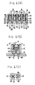
- FIG. 3(A) and FIG. 3(B) show female terminals which are inserted into the housing 12 through the opening 18.
- a female terminal 40 of this embodiment is formed by being punched from a blank 38 made of electrically and mechanically preferable metal such as bronze.
- a blank 38 made of electrically and mechanically preferable metal such as bronze.
- an inner side portion contacting with the male terminal 6, that is, a contact which will be described later, is subjected to so-called shaving so as to be formed into a flat surface. This serves to prevent the male terminal 6 from being damaged when contacting with the male terminal 6.
- the female terminal 40 has a flat shape as shown by a reference numeral 40a in the left-hand side of FIG. 3(A) and FIG. 3(B).
- each of the female terminals 40 has a plate like base section 42, a pair of arm sections 44 extending from the base section, and a contact section 46 provided on the distal end of the respective arm sections 44.
- a solder tail 48 extends from a lower side of the base section 42, that is, to a side opposite to the arm section 44.
- the female terminal 40 is supported onto the blank 38 through tail section 48.
- a middle tongue section 50 extends from the base section 42 between the paired arm sections 44, 44.
- the middle tongue section 50 has a distal end formed into taper, and is formed with a plurality of small projections 52 projecting from its circumferential portion.
- the small projection 52 projects along the surface direction on the same plane as the middle tongue section 50.
- the small projection 52 is not limited to this, and may be extended in a thickness direction or in both thickness and surface directions.
- the female terminal 40 is bent from the flat shape as shown by the reference numeral 40a into the solid shape as shown by the reference numeral 40b. In such a bent state, the paired arm sections 44 is bent so as to be inclined with respect to the plane where the base section 42 and the middle tongue section 50 are arranged.
- the contact section 48 is offset in a thickness direction so as to be substantially parallel with the base section 42 and the middle tongue section 50.
- FIG. 4 shows a state in which the aforesaid female terminal 40 is fitted into the housing 12.
- Each of the female terminals 40 is inserted into the housing 12 through the opening 18, and then, the middle tongue section 50 thereof is inserted into the slot 32 (see FIG. 2(C) and (D)) formed in the side wall portion 20.
- Small projections 52 formed at the periphery of the middle tongue section 50 bite into the housing material to firmly retain the female terminal in the housing 12.
- the middle tongue section 50 is inserted into the slot 32, the base section 42 is retained on the recess portion 22 which is formed as a retaining portion of the side wall portion 20.
- the female terminal 40 does not project into the insertion slot 14.
- both edge portions of the base section may bite into their neighborhood wall portions 24 and 26. By doing this, the female terminal 40 can be more firmly retained.
- Arm sections 44,44 are individually received in guide grooves 28 and 30 formed in the side wall portions 24 and 26. These arm sections 44,44 extend along the guide groove 28 and 30 from the base section 42 received in the retaining portion, that is, in the recess portion 22, in a state of being inclined with respect to the axial line of the insertion slot 14.
- Contact sections 46 on the distal end of the arm sections between portion 44 is situated on the intermediate position the side wall portion 20 formed with the recess 22 and the slot 32 and the opposed side wall (see FIG. 1(B)).
- the respective arm sections 44, 44 are slidable in the guide grooves 28 and 30 along directions in which these contact sections 46 is closed to and away from the axis of the insertion slot 14. ordinarily, these contact portions 46,46 are arranged in a state of projecting into the insertion slot 14. It is possible to form the solder tail section 48 into a proper shape. In case of bending the solder tail section 48 as shown in FIG. 1(B), when the solder tail sections 48 are inserted into a through hole of the printed circuit board P, it is possible to momentarily hold these solder tail sections 48 on the printed circuit board P.
- FIG. 5(A) and FIG. 5(B) individually show a cross section of the male connector 8 paring with the female connector 10 as described above.
- the male connector 8 has 22 male terminals comprising a square-section pins which is the same number as the female terminal 40.
- Liquid crystal polymer (LCP) is applied onto the circumference of respective male terminals 6 by injection molding.
- the male terminal 6 has a small diameter portion for preventing it from coming off at its intermediate portion.
- the male terminal has a tapered distal end portion.
- a side of the square section of the male terminal has a length of a substantially half of a side of the square section of the insertion slot 14.
- the male terminal 6 is inserted coaxially with the axis of the insertion slot 14, and the distal end portion thereof reaches between opposed contact sections 45 and 46. And then, when a distance between contact sections 46 and 46 is widened by means of the inserted male terminal 6, arm sections 44, 44 slide in the guide grooves 28 and 30.
- the male terminal 6 When the male terminal i further inserted into the insertion slot 14, the male terminal 6 is pressed from its both side by contact sections 46 and 46 in a state of being held therebetween, so that it is electrically connected with the female terminal 40 while being mechanically connected therewith by a spring force of the arm sections 44, 44. Also, since the base section 42 is retained in the recess portion 22 of the side wall portion 20, the male terminal does not interfere with the base section 42 even if being inserted into the inner part. Therefore, there is no need of making large the dimension of the female terminal 40 and the housing 12 of the female connector 10. Moreover, it is possible to electrically and mechanically connect the male connector 8 with female connector 10 in a state of inserting the longer male terminal 6 by the innermost position of the female terminal.
- the middle tongue section 50 is inserted into the slot 32 (see FIG. 2(C)).
- a rotational force acting on the female terminal 40 is offset by means of the middle tongue section 50; therefore, the female terminal 40 does not come off from the housing 12.
- the male terminal 6 Even if the male terminal 6 is inserted into the insertion slot 14 in a state of being inclined with respect to the axis of the insertion slot 14 as shown in the left-hand side of FIG. 6(A) and FIG. 6(B), the male terminal 6 necessarily contacts with the contact section 46 as shown in FIG. 6(C) because its distal end portion is formed so that a side of the square section of the male terminal has a length of a substantially half of a side of the square section of the insertion slot 14. Thus, it is possible to guide arm sections 44 into guide grooves 28 and 30 via the contact section 46. Therefore, the male or female terminal can be prevented from being damaged due to an engagement of the contact sections 46 and the male terminal 6.
- the electrical connector according to the present device is constructed in the following manner. Namely, the base section of the female terminal is received in the retaining portion recessed on one of side wall portions partitioning the insertion slot of the male terminal, and the arm sections supporting the contact sections extend in a state of being inclined with respect to the axial line of the insertion slot. Moreover, since the contact sections are situated on the intermediate position between the side wall portion recessed the retaining portion and the opposed side wall portion, the base section is arranged in a position shifting from the axial line of the insertion slot.
- the housing has guide grooves which receive the arm sections and are individually formed on opposed side wall portions on both side of the side wall portion formed with a recess portion of being the retaining portion, the arm sections of the female terminal slide on the guide grooves, so that the spring effect of arm sections can be securely exhibited.
- the male terminal can be securely held by the elastic force.
- the housing is further formed with slots which have one end opening to the retaining portion and extend toward one side of the housing along the axial line of the insertion slot 14 in the side wall portion it recessing the retaining portion.
- the female terminal has a middle tongue section extending from the base section between the paired arm sections.
- the middle tongue section When the base section of the female terminal is received in the retaining portion of the housing, the middle tongue section thereof is retained in the slots of the housing.
- the middle tongue section serves to prevent the rotation of the base section, so that the base section can be securely retained in the retaining portion.
- the middle tongue section is formed with a plurality of small projections at its periphery. These small projections bite into the housing material so that the female terminal is firmly held in the housing. Thus, the female terminal can be prevented from coming off from the housing.
Landscapes
- Coupling Device And Connection With Printed Circuit (AREA)
- Connector Housings Or Holding Contact Members (AREA)
Claims (5)
- Ein weiblicher Anschluss (40) für einen elektrischen Verbinder (10) aufweisend:a. ein Paar von Kontaktbereichen (46), die in einen Einfügeschlitz (14) eines Gehäuses (12) hineinragen;b. einen Basisbereich (42), welcher die Kontaktbereiche (46) über ein paar Armbereiche (44) trägt;c. wobei sich die Armbereiche (44) in einem in Bezug auf die axiale Linie des Einfügeschlitzes (14) geneigten Zustand von dem Basisbereich (42) aus erstrecken, dadurch gekennzeichnet, dass sie weiterhin einen mittleren Zungenbereich (50) aufweisen, der sich zwischen dem Paar von Kontaktbereichen (46) von dem Basisbereich (42) aus erstreckt, um in einen Halteschlitz (32) des Gehäuses (12) eingefügt zu werden, der entlang seiner Axiallinie offen ist.
- Der weibliche Anschluss (40) gemäß Anspruch 1, dadurch gekennzeichnet, dass der mittlere Zungenbereich (50) an seiner Außenfläche eine Mehrzahl von Vorsprüngen (52) zum Verrasten in dem Gehäuse (12) aufweist.
- Ein Gehäuse (12) für einen elektrischen Verbinder (10), hergestellt aus einem isolierenden Material aufweisend:a. eine Mehrzahl von Einfügeschlitzen (14) zur Aufnahme von männlichen Anschlüssen (6), wobei jeder ein Paar gegenüberliegender Seiten (24, 26) und ein offenes Ende aufweist;b. ein weiblicher Anschluss (40) gemäß den Ansprüchen 1 oder 2, dadurch gekennzeichnet, dass er weiterhin aufweist:c. einen Haltebereich (22) um den Basisbereich (42) des weiblichen Anschlusses (40) festzuhalten;d. einen Schlitz (32), um den mittleren Zungenbereich (50) des weiblichen Anschlusses (40) zu halten, wobei der Schlitz (32) ein offenes Ende in dem Aussparungsbereich (22) aufweist und sich in Richtung des offenen Endes des Einfügeschlitzes (14) erstreckt und entlang seiner Axiallinie offen ist.
- Das Gehäuse gemäß Anspruch 3, weiterhin Führungsnute (28, 30) aufweisend, die in dem Paar gegenüberliegender Seiten (24, 26) eingeformt sind und sich von dem Haltebereich (22) aus erstrecken, um das Paar von Armbereichen (44) des weiblichen Anschlusses (40) aufzunehmen und zu führen.
- Das Gehäuse gemäß Anspruch 3 oder 4, wobei das Paar von Kontaktbereichen (46) des weiblichen Anschlusses (40) in den Führungsnuten (28, 30) gleitbar ist.
Applications Claiming Priority (3)
| Application Number | Priority Date | Filing Date | Title |
|---|---|---|---|
| JP4949/97U | 1997-06-11 | ||
| JP1997004949U JP3044293U (ja) | 1997-06-11 | 1997-06-11 | 電気コネクタ |
| JP494997U | 1997-06-11 |
Publications (3)
| Publication Number | Publication Date |
|---|---|
| EP0884802A2 EP0884802A2 (de) | 1998-12-16 |
| EP0884802A3 EP0884802A3 (de) | 1999-11-24 |
| EP0884802B1 true EP0884802B1 (de) | 2003-05-07 |
Family
ID=11597834
Family Applications (1)
| Application Number | Title | Priority Date | Filing Date |
|---|---|---|---|
| EP98110174A Expired - Lifetime EP0884802B1 (de) | 1997-06-11 | 1998-06-04 | Terminal und Gehäuse mit Terminal |
Country Status (5)
| Country | Link |
|---|---|
| US (1) | US6109974A (de) |
| EP (1) | EP0884802B1 (de) |
| JP (1) | JP3044293U (de) |
| DE (1) | DE69814234T2 (de) |
| TW (1) | TW380760U (de) |
Families Citing this family (3)
| Publication number | Priority date | Publication date | Assignee | Title |
|---|---|---|---|---|
| TWI259182B (en) | 1998-11-17 | 2006-08-01 | Cytec Tech Corp | Process for preparing triazines using a combination of Lewis acids with reaction promoters |
| US6475042B1 (en) * | 2001-12-10 | 2002-11-05 | Hon Hai Precision Ind. Co., Ltd. | High-speed electrical connector |
| CN201667429U (zh) * | 2009-11-12 | 2010-12-08 | 富士康(昆山)电脑接插件有限公司 | 电连接器 |
Family Cites Families (11)
| Publication number | Priority date | Publication date | Assignee | Title |
|---|---|---|---|---|
| US2683259A (en) * | 1950-08-21 | 1954-07-06 | Mcmurdo Instr Company Ltd | Radio valve holder |
| GB768242A (en) * | 1954-02-01 | 1957-02-13 | Edison Swan Electric Co Ltd | Improvements relating to the manufacture of electrical socket contacts |
| US3865462A (en) * | 1973-03-07 | 1975-02-11 | Amp Inc | Preloaded contact and latchable housing assembly |
| US4175821A (en) * | 1978-05-15 | 1979-11-27 | Teradyne, Inc. | Electrical connector |
| US4241970A (en) * | 1979-04-09 | 1980-12-30 | Amp Incorporated | Electrical connector having improved receptacle terminal |
| US4781612A (en) * | 1983-12-14 | 1988-11-01 | Amp Incorporated | Socket for single in-line memory module |
| JPS6358776A (ja) * | 1986-08-27 | 1988-03-14 | アンプ インコ−ポレ−テツド | レセプタクルコンタクト |
| AU6402290A (en) * | 1990-09-12 | 1992-03-30 | Thomas & Betts, France | Female connector with double-strip contacts |
| US5183421A (en) * | 1991-07-24 | 1993-02-02 | Foxconn International, Inc. | Connector contact and method of manufacture |
| US5409406A (en) * | 1993-12-17 | 1995-04-25 | Berg Technology, Inc. | Connector for high density electronic assemblies |
| DE69518157T2 (de) * | 1995-12-01 | 2001-03-29 | Berg Electronics Mfg | Glatte Kontaktelemente, Verfahren zur Herstellung solcher Elemente und Produkte mit solchen Elementen |
-
1997
- 1997-06-11 JP JP1997004949U patent/JP3044293U/ja not_active Expired - Lifetime
-
1998
- 1998-05-26 US US09/084,658 patent/US6109974A/en not_active Expired - Fee Related
- 1998-06-04 DE DE69814234T patent/DE69814234T2/de not_active Expired - Lifetime
- 1998-06-04 EP EP98110174A patent/EP0884802B1/de not_active Expired - Lifetime
- 1998-06-04 TW TW087208822U patent/TW380760U/zh unknown
Also Published As
| Publication number | Publication date |
|---|---|
| EP0884802A2 (de) | 1998-12-16 |
| DE69814234D1 (de) | 2003-06-12 |
| DE69814234T2 (de) | 2004-02-19 |
| TW380760U (en) | 2000-01-21 |
| EP0884802A3 (de) | 1999-11-24 |
| US6109974A (en) | 2000-08-29 |
| JP3044293U (ja) | 1997-12-16 |
Similar Documents
| Publication | Publication Date | Title |
|---|---|---|
| US7862358B2 (en) | Electrical connector | |
| US6821158B2 (en) | Connector | |
| US5240430A (en) | Electrical connector for cable to circit board application | |
| US6234827B1 (en) | Electrical connector shield with dual function of mechanical locking and electrical shielding continuety | |
| US5122066A (en) | Electrical terminal with means to insure that a positive electrical connection is effected | |
| JP2724657B2 (ja) | 低プロフィルの電気コネクタ | |
| JPH05326058A (ja) | 薄型電気コネクタ | |
| US6086418A (en) | Electrical connector | |
| US6135816A (en) | Electrical connector having an improved construction for fixing shield plates to a receptacle connector | |
| EP0540260B1 (de) | Elektrischer Verbinder zur Verbindung einer Leiterplatte mit einem Kabel | |
| JP3424150B2 (ja) | 電気コネクタ | |
| US7112072B2 (en) | Ground bus for an electrical connector | |
| US7188408B2 (en) | Method of making a straddle mount connector | |
| US6796825B2 (en) | Electrical connector for attaching a circuit board | |
| US20070066105A1 (en) | Electrical connector | |
| US7261597B2 (en) | Electrical connector with low profile | |
| US6435892B1 (en) | Electrical connector with a supporting mechanism | |
| US20050130506A1 (en) | Connector | |
| US6227898B1 (en) | Card edge connector with removable rail guide | |
| US6666711B2 (en) | Electrical connector for a circuit board | |
| WO2007015339A1 (ja) | 電気コネクタ | |
| EP0884802B1 (de) | Terminal und Gehäuse mit Terminal | |
| JP2002141124A (ja) | 基板取付型コネクタおよびコネクタの基板取付構造 | |
| US6764316B1 (en) | Straddle-mount electrical connector | |
| US6168473B1 (en) | Clamping structure for communication connector |
Legal Events
| Date | Code | Title | Description |
|---|---|---|---|
| PUAI | Public reference made under article 153(3) epc to a published international application that has entered the european phase |
Free format text: ORIGINAL CODE: 0009012 |
|
| AK | Designated contracting states |
Kind code of ref document: A2 Designated state(s): DE FR GB IE SE |
|
| AX | Request for extension of the european patent |
Free format text: AL;LT;LV;MK;RO;SI |
|
| PUAL | Search report despatched |
Free format text: ORIGINAL CODE: 0009013 |
|
| AK | Designated contracting states |
Kind code of ref document: A3 Designated state(s): AT BE CH CY DE DK ES FI FR GB GR IE IT LI LU MC NL PT SE |
|
| AX | Request for extension of the european patent |
Free format text: AL;LT;LV;MK;RO;SI |
|
| 17P | Request for examination filed |
Effective date: 20000405 |
|
| AKX | Designation fees paid |
Free format text: DE FR GB IE SE |
|
| 17Q | First examination report despatched |
Effective date: 20001027 |
|
| GRAG | Despatch of communication of intention to grant |
Free format text: ORIGINAL CODE: EPIDOS AGRA |
|
| RIC1 | Information provided on ipc code assigned before grant |
Free format text: 7H 01R 13/115 A, 7H 01R 12/22 B |
|
| RTI1 | Title (correction) |
Free format text: TERMINAL ET BOITIER COMPRENANT LE TERMINAL |
|
| GRAG | Despatch of communication of intention to grant |
Free format text: ORIGINAL CODE: EPIDOS AGRA |
|
| GRAH | Despatch of communication of intention to grant a patent |
Free format text: ORIGINAL CODE: EPIDOS IGRA |
|
| GRAH | Despatch of communication of intention to grant a patent |
Free format text: ORIGINAL CODE: EPIDOS IGRA |
|
| GRAA | (expected) grant |
Free format text: ORIGINAL CODE: 0009210 |
|
| AK | Designated contracting states |
Designated state(s): DE FR GB IE SE |
|
| REG | Reference to a national code |
Ref country code: GB Ref legal event code: FG4D |
|
| PG25 | Lapsed in a contracting state [announced via postgrant information from national office to epo] |
Ref country code: IE Free format text: LAPSE BECAUSE OF NON-PAYMENT OF DUE FEES Effective date: 20030604 |
|
| REG | Reference to a national code |
Ref country code: IE Ref legal event code: FG4D |
|
| REF | Corresponds to: |
Ref document number: 69814234 Country of ref document: DE Date of ref document: 20030612 Kind code of ref document: P |
|
| PG25 | Lapsed in a contracting state [announced via postgrant information from national office to epo] |
Ref country code: SE Free format text: LAPSE BECAUSE OF FAILURE TO SUBMIT A TRANSLATION OF THE DESCRIPTION OR TO PAY THE FEE WITHIN THE PRESCRIBED TIME-LIMIT Effective date: 20030807 |
|
| ET | Fr: translation filed | ||
| PLBE | No opposition filed within time limit |
Free format text: ORIGINAL CODE: 0009261 |
|
| STAA | Information on the status of an ep patent application or granted ep patent |
Free format text: STATUS: NO OPPOSITION FILED WITHIN TIME LIMIT |
|
| REG | Reference to a national code |
Ref country code: IE Ref legal event code: MM4A |
|
| 26N | No opposition filed |
Effective date: 20040210 |
|
| PGFP | Annual fee paid to national office [announced via postgrant information from national office to epo] |
Ref country code: FR Payment date: 20080606 Year of fee payment: 11 |
|
| PGFP | Annual fee paid to national office [announced via postgrant information from national office to epo] |
Ref country code: GB Payment date: 20080616 Year of fee payment: 11 |
|
| GBPC | Gb: european patent ceased through non-payment of renewal fee |
Effective date: 20090604 |
|
| REG | Reference to a national code |
Ref country code: FR Ref legal event code: ST Effective date: 20100226 |
|
| PG25 | Lapsed in a contracting state [announced via postgrant information from national office to epo] |
Ref country code: FR Free format text: LAPSE BECAUSE OF NON-PAYMENT OF DUE FEES Effective date: 20090630 |
|
| PG25 | Lapsed in a contracting state [announced via postgrant information from national office to epo] |
Ref country code: GB Free format text: LAPSE BECAUSE OF NON-PAYMENT OF DUE FEES Effective date: 20090604 |
|
| PGFP | Annual fee paid to national office [announced via postgrant information from national office to epo] |
Ref country code: DE Payment date: 20120629 Year of fee payment: 15 |
|
| REG | Reference to a national code |
Ref country code: DE Ref legal event code: R119 Ref document number: 69814234 Country of ref document: DE |
|
| PG25 | Lapsed in a contracting state [announced via postgrant information from national office to epo] |
Ref country code: DE Free format text: LAPSE BECAUSE OF NON-PAYMENT OF DUE FEES Effective date: 20140101 |
|
| REG | Reference to a national code |
Ref country code: DE Ref legal event code: R079 Ref document number: 69814234 Country of ref document: DE Free format text: PREVIOUS MAIN CLASS: H01R0013115000 Ipc: H01R0013110000 |
|
| REG | Reference to a national code |
Ref country code: DE Ref legal event code: R119 Ref document number: 69814234 Country of ref document: DE Effective date: 20140101 Ref country code: DE Ref legal event code: R079 Ref document number: 69814234 Country of ref document: DE Free format text: PREVIOUS MAIN CLASS: H01R0013115000 Ipc: H01R0013110000 Effective date: 20140701 |