EP0878984B1 - Magnetic prepreg, its manufacturing method and printed wiring board employing the prepreg - Google Patents
Magnetic prepreg, its manufacturing method and printed wiring board employing the prepreg Download PDFInfo
- Publication number
- EP0878984B1 EP0878984B1 EP97939168A EP97939168A EP0878984B1 EP 0878984 B1 EP0878984 B1 EP 0878984B1 EP 97939168 A EP97939168 A EP 97939168A EP 97939168 A EP97939168 A EP 97939168A EP 0878984 B1 EP0878984 B1 EP 0878984B1
- Authority
- EP
- European Patent Office
- Prior art keywords
- magnetic
- prepreg
- circuit board
- printed circuit
- soft magnetic
- Prior art date
- Legal status (The legal status is an assumption and is not a legal conclusion. Google has not performed a legal analysis and makes no representation as to the accuracy of the status listed.)
- Expired - Lifetime
Links
- 238000004519 manufacturing process Methods 0.000 title description 2
- 229920005989 resin Polymers 0.000 claims abstract description 21
- 239000011347 resin Substances 0.000 claims abstract description 21
- 239000004744 fabric Substances 0.000 claims abstract description 14
- 239000011521 glass Substances 0.000 claims abstract description 13
- 229920001187 thermosetting polymer Polymers 0.000 claims abstract description 12
- 239000003822 epoxy resin Substances 0.000 claims abstract description 6
- 229920000647 polyepoxide Polymers 0.000 claims abstract description 6
- 238000000034 method Methods 0.000 claims description 10
- 239000003973 paint Substances 0.000 claims description 9
- 239000000843 powder Substances 0.000 claims description 8
- 239000002184 metal Substances 0.000 claims description 4
- 229910052751 metal Inorganic materials 0.000 claims description 4
- 239000006247 magnetic powder Substances 0.000 abstract description 14
- 239000000463 material Substances 0.000 abstract description 5
- 239000002245 particle Substances 0.000 abstract description 2
- 239000011248 coating agent Substances 0.000 abstract 1
- 238000000576 coating method Methods 0.000 abstract 1
- 230000005684 electric field Effects 0.000 description 8
- RYGMFSIKBFXOCR-UHFFFAOYSA-N Copper Chemical compound [Cu] RYGMFSIKBFXOCR-UHFFFAOYSA-N 0.000 description 6
- 239000011889 copper foil Substances 0.000 description 5
- 230000008878 coupling Effects 0.000 description 5
- 238000010168 coupling process Methods 0.000 description 5
- 238000005859 coupling reaction Methods 0.000 description 5
- 239000011230 binding agent Substances 0.000 description 3
- 239000004020 conductor Substances 0.000 description 3
- 230000000694 effects Effects 0.000 description 3
- 229910021364 Al-Si alloy Inorganic materials 0.000 description 2
- 238000001035 drying Methods 0.000 description 2
- 230000035699 permeability Effects 0.000 description 2
- 230000008569 process Effects 0.000 description 2
- 230000009467 reduction Effects 0.000 description 2
- XNWFRZJHXBZDAG-UHFFFAOYSA-N 2-METHOXYETHANOL Chemical compound COCCO XNWFRZJHXBZDAG-UHFFFAOYSA-N 0.000 description 1
- 229910001030 Iron–nickel alloy Inorganic materials 0.000 description 1
- 230000002411 adverse Effects 0.000 description 1
- 229910045601 alloy Inorganic materials 0.000 description 1
- 239000000956 alloy Substances 0.000 description 1
- 150000001408 amides Chemical class 0.000 description 1
- 230000015572 biosynthetic process Effects 0.000 description 1
- 238000006243 chemical reaction Methods 0.000 description 1
- 229910052802 copper Inorganic materials 0.000 description 1
- 239000010949 copper Substances 0.000 description 1
- 238000010586 diagram Methods 0.000 description 1
- QGBSISYHAICWAH-UHFFFAOYSA-N dicyandiamide Chemical compound NC(N)=NC#N QGBSISYHAICWAH-UHFFFAOYSA-N 0.000 description 1
- XXBDWLFCJWSEKW-UHFFFAOYSA-N dimethylbenzylamine Chemical compound CN(C)CC1=CC=CC=C1 XXBDWLFCJWSEKW-UHFFFAOYSA-N 0.000 description 1
- 230000005674 electromagnetic induction Effects 0.000 description 1
- 150000003949 imides Chemical class 0.000 description 1
- 230000003993 interaction Effects 0.000 description 1
- 230000009545 invasion Effects 0.000 description 1
- 239000000696 magnetic material Substances 0.000 description 1
- 230000007257 malfunction Effects 0.000 description 1
- 239000000203 mixture Substances 0.000 description 1
- 229920003986 novolac Polymers 0.000 description 1
- 230000001590 oxidative effect Effects 0.000 description 1
- 229910000889 permalloy Inorganic materials 0.000 description 1
- 239000005011 phenolic resin Substances 0.000 description 1
- 229920001721 polyimide Polymers 0.000 description 1
- 230000005855 radiation Effects 0.000 description 1
- 238000009877 rendering Methods 0.000 description 1
- 238000012216 screening Methods 0.000 description 1
- 229910000702 sendust Inorganic materials 0.000 description 1
- 239000011877 solvent mixture Substances 0.000 description 1
- 238000001228 spectrum Methods 0.000 description 1
- 239000000758 substrate Substances 0.000 description 1
- 229920002803 thermoplastic polyurethane Polymers 0.000 description 1
- 238000002834 transmittance Methods 0.000 description 1
Images


Classifications
-
- H—ELECTRICITY
- H05—ELECTRIC TECHNIQUES NOT OTHERWISE PROVIDED FOR
- H05K—PRINTED CIRCUITS; CASINGS OR CONSTRUCTIONAL DETAILS OF ELECTRIC APPARATUS; MANUFACTURE OF ASSEMBLAGES OF ELECTRICAL COMPONENTS
- H05K1/00—Printed circuits
- H05K1/02—Details
- H05K1/03—Use of materials for the substrate
-
- H—ELECTRICITY
- H05—ELECTRIC TECHNIQUES NOT OTHERWISE PROVIDED FOR
- H05K—PRINTED CIRCUITS; CASINGS OR CONSTRUCTIONAL DETAILS OF ELECTRIC APPARATUS; MANUFACTURE OF ASSEMBLAGES OF ELECTRICAL COMPONENTS
- H05K9/00—Screening of apparatus or components against electric or magnetic fields
- H05K9/0007—Casings
- H05K9/002—Casings with localised screening
- H05K9/0039—Galvanic coupling of ground layer on printed circuit board [PCB] to conductive casing
-
- B—PERFORMING OPERATIONS; TRANSPORTING
- B29—WORKING OF PLASTICS; WORKING OF SUBSTANCES IN A PLASTIC STATE IN GENERAL
- B29C—SHAPING OR JOINING OF PLASTICS; SHAPING OF MATERIAL IN A PLASTIC STATE, NOT OTHERWISE PROVIDED FOR; AFTER-TREATMENT OF THE SHAPED PRODUCTS, e.g. REPAIRING
- B29C70/00—Shaping composites, i.e. plastics material comprising reinforcements, fillers or preformed parts, e.g. inserts
- B29C70/02—Shaping composites, i.e. plastics material comprising reinforcements, fillers or preformed parts, e.g. inserts comprising combinations of reinforcements, e.g. non-specified reinforcements, fibrous reinforcing inserts and fillers, e.g. particulate fillers, incorporated in matrix material, forming one or more layers and with or without non-reinforced or non-filled layers
- B29C70/021—Combinations of fibrous reinforcement and non-fibrous material
- B29C70/025—Combinations of fibrous reinforcement and non-fibrous material with particular filler
-
- C—CHEMISTRY; METALLURGY
- C08—ORGANIC MACROMOLECULAR COMPOUNDS; THEIR PREPARATION OR CHEMICAL WORKING-UP; COMPOSITIONS BASED THEREON
- C08J—WORKING-UP; GENERAL PROCESSES OF COMPOUNDING; AFTER-TREATMENT NOT COVERED BY SUBCLASSES C08B, C08C, C08F, C08G or C08H
- C08J5/00—Manufacture of articles or shaped materials containing macromolecular substances
- C08J5/24—Impregnating materials with prepolymers which can be polymerised in situ, e.g. manufacture of prepregs
- C08J5/241—Impregnating materials with prepolymers which can be polymerised in situ, e.g. manufacture of prepregs using inorganic fibres
- C08J5/244—Impregnating materials with prepolymers which can be polymerised in situ, e.g. manufacture of prepregs using inorganic fibres using glass fibres
-
- C—CHEMISTRY; METALLURGY
- C08—ORGANIC MACROMOLECULAR COMPOUNDS; THEIR PREPARATION OR CHEMICAL WORKING-UP; COMPOSITIONS BASED THEREON
- C08J—WORKING-UP; GENERAL PROCESSES OF COMPOUNDING; AFTER-TREATMENT NOT COVERED BY SUBCLASSES C08B, C08C, C08F, C08G or C08H
- C08J5/00—Manufacture of articles or shaped materials containing macromolecular substances
- C08J5/24—Impregnating materials with prepolymers which can be polymerised in situ, e.g. manufacture of prepregs
- C08J5/249—Impregnating materials with prepolymers which can be polymerised in situ, e.g. manufacture of prepregs characterised by the additives used in the prepolymer mixture
-
- H—ELECTRICITY
- H05—ELECTRIC TECHNIQUES NOT OTHERWISE PROVIDED FOR
- H05K—PRINTED CIRCUITS; CASINGS OR CONSTRUCTIONAL DETAILS OF ELECTRIC APPARATUS; MANUFACTURE OF ASSEMBLAGES OF ELECTRICAL COMPONENTS
- H05K1/00—Printed circuits
- H05K1/02—Details
- H05K1/0213—Electrical arrangements not otherwise provided for
- H05K1/0216—Reduction of cross-talk, noise or electromagnetic interference
- H05K1/023—Reduction of cross-talk, noise or electromagnetic interference using auxiliary mounted passive components or auxiliary substances
- H05K1/0233—Filters, inductors or a magnetic substance
-
- H—ELECTRICITY
- H05—ELECTRIC TECHNIQUES NOT OTHERWISE PROVIDED FOR
- H05K—PRINTED CIRCUITS; CASINGS OR CONSTRUCTIONAL DETAILS OF ELECTRIC APPARATUS; MANUFACTURE OF ASSEMBLAGES OF ELECTRICAL COMPONENTS
- H05K1/00—Printed circuits
- H05K1/02—Details
- H05K1/03—Use of materials for the substrate
- H05K1/0313—Organic insulating material
- H05K1/0353—Organic insulating material consisting of two or more materials, e.g. two or more polymers, polymer + filler, + reinforcement
- H05K1/0373—Organic insulating material consisting of two or more materials, e.g. two or more polymers, polymer + filler, + reinforcement containing additives, e.g. fillers
-
- B—PERFORMING OPERATIONS; TRANSPORTING
- B29—WORKING OF PLASTICS; WORKING OF SUBSTANCES IN A PLASTIC STATE IN GENERAL
- B29K—INDEXING SCHEME ASSOCIATED WITH SUBCLASSES B29B, B29C OR B29D, RELATING TO MOULDING MATERIALS OR TO MATERIALS FOR MOULDS, REINFORCEMENTS, FILLERS OR PREFORMED PARTS, e.g. INSERTS
- B29K2995/00—Properties of moulding materials, reinforcements, fillers, preformed parts or moulds
- B29K2995/0003—Properties of moulding materials, reinforcements, fillers, preformed parts or moulds having particular electrical or magnetic properties, e.g. piezoelectric
- B29K2995/0008—Magnetic or paramagnetic
-
- H—ELECTRICITY
- H05—ELECTRIC TECHNIQUES NOT OTHERWISE PROVIDED FOR
- H05K—PRINTED CIRCUITS; CASINGS OR CONSTRUCTIONAL DETAILS OF ELECTRIC APPARATUS; MANUFACTURE OF ASSEMBLAGES OF ELECTRICAL COMPONENTS
- H05K2201/00—Indexing scheme relating to printed circuits covered by H05K1/00
- H05K2201/08—Magnetic details
- H05K2201/083—Magnetic materials
- H05K2201/086—Magnetic materials for inductive purposes, e.g. printed inductor with ferrite core
-
- Y—GENERAL TAGGING OF NEW TECHNOLOGICAL DEVELOPMENTS; GENERAL TAGGING OF CROSS-SECTIONAL TECHNOLOGIES SPANNING OVER SEVERAL SECTIONS OF THE IPC; TECHNICAL SUBJECTS COVERED BY FORMER USPC CROSS-REFERENCE ART COLLECTIONS [XRACs] AND DIGESTS
- Y10—TECHNICAL SUBJECTS COVERED BY FORMER USPC
- Y10T—TECHNICAL SUBJECTS COVERED BY FORMER US CLASSIFICATION
- Y10T428/00—Stock material or miscellaneous articles
- Y10T428/24—Structurally defined web or sheet [e.g., overall dimension, etc.]
- Y10T428/24802—Discontinuous or differential coating, impregnation or bond [e.g., artwork, printing, retouched photograph, etc.]
- Y10T428/24926—Discontinuous or differential coating, impregnation or bond [e.g., artwork, printing, retouched photograph, etc.] including ceramic, glass, porcelain or quartz layer
Definitions
- the present invention relates to a printed circuit board and, in particular, to a printed circuit board which suppresses electromagnetic interference caused by interference of undesired electromagnetic waves.
- a digital electronic device comprises a number of electronic components, such as a random access memory (RAM), a read-only memory (ROM), a microprocessor, and the like each of which comprises a number of logic elements. These electronic components are mounted on a printed circuit board having signal lines (wired conductors) wired around thereon.
- the operation speed of the logic elements has been rapidly increased and further the reduction in weight, thickness, length and size of the device has also been highly advanced. Following this, the mounting density of the electronic components onto the printed circuit board has also been rapidly enhanced.
- the electronic component is a noise generation source which generates high frequency noise.
- the high frequency noise causes interactions cooperatively with crosstalk noise or noise due to impedance mismatch so as to induce malfunctions relative to other electronic components on the printed circuit board and adversely affect other systems.
- electrostatic coupling between the electronic components and between the signal lines is increased so that the electromagnetic interference is liable to occur in the digital electronic device.
- the foregoing electromagnetic wave shield circuit board has a structure wherein two circuit board surfaces are opposite to each other with the shield layer interposed therebetween.
- the shield layer is formed of a conductor material which reflects the electromagnetic waves.
- a shield effect can be expected with respect to one circuit board surface confronting the opposite circuit board surface on the side where an electronic component to be a noise generation source is installed, while, with respect to the opposite circuit board surface on the side where the electronic component to be the noise generation source is installed, undesired radiation is generated due to the reflection of the electromagnetic waves is generated.
- secondary electromagnetic coupling is promoted at the opposite circuit board surface on the side of the noise generation source.
- the shield layer works as an antenna, secondary radiant noise is possibly generated from the shield layer.
- JP-A-8-46386 (hereinafter referred to as the prior art), the applicant of this application has offered a printed circuit board which does not spoil a shield effect of an electromagnetic wave shield circuit board and thus has a sufficient shield effect against transmittance of the electromagnetic waves, while, with respect to reflection of the electromagnetic waves, does not promote electromagnetic coupling at least due to reflection.
- a printed circuit base member having wired conductors on one side or both sides thereof comprises a conductive support and insulating soft magnetic layers provided on both sides of the conductive support.
- the insulating soft magnetic layer includes soft magnetic powder and an organic binding agent. Further, the insulating soft magnetic layer may have a dielectric layer on at least one side thereof.
- This dielectric layer includes dielectric powder and an organic binding agent.
- the foregoing insulating soft magnetic layer may include the soft magnetic powder, the dielectric powder and the organic binding agent. It is preferable that the foregoing soft magnetic powder is powder being flat and/or needle-shaped.
- a stacked body (electromagnetic interference suppressing layer) of the conductive support and the insulating soft magnetic body to be used in the foregoing printed circuit base member is produced, for example, in the following manner: Copper paste is formed into films on both sides of a polyimide film of 75 ⁇ m by a doctor blade process to obtain a conductive support. Thereafter, soft magnetic paste is applied onto both sides of the conductive support by the doctor blade process to form insulating soft magnetic layers, which are then subjected to curing at 85°C for 24 hours to obtain a printed circuit base member.
- JP-A-02 120 040 also discloses a magnetic prepreg, a method of producing it and a printed circuit board using the magnetic prepreg.
- a prepreg constituting a printed circuit board is composed of resin and glass cloth.
- the conventional prepreg is produced by impregnating thermosetting resin into a glass cloth and then drying and half-curing it.
- JP-A-02 087 593 discloses magnetic prepregs used for all boards 11, 14 and 15.
- JP-A-08 186 378 discloses a prepreg 4a dipped with a magnetic material, and stacked to a side of a normal prepreg 3a, which itself is stacked via a wiring pattern 2 to a side of a plate or substrate 1.
- a theme of the present invention is to provide a magnetic prepreg which can absorb the radiant noise.
- Another theme of the present invention is to provide a method of producing the foregoing magnetic prepreg.
- Still another theme of the present invention is to provide a printed circuit board using the foregoing magnetic prepreg.
- a magnetic prepreg 10 is formed by impregnating a magnetic paint 12 composed of soft magnetic powder 121 and thermosetting resin 122 into a glass cloth 14. It is preferable that the soft magnetic powder 121 is metal powder being substantially flat. Further, it is preferable that a main component of the thermosetting resin 122 is epoxy resin.
- thermosetting resin 122 (poly) urethane resin, phenol resin, amide resin, imide resin or the like can be cited other than the epoxy resin.
- soft magnetic powder 12 an Fe-Al-Si alloy (this is called Sendust (trademark)) or an Fe-Ni alloy (Permalloy) having a large high frequency permeability can be cited as a typical material thereof.
- the soft magnetic powder 12 is used by being finely powdered and by oxidizing surface portions thereof. It is preferable that an aspect ratio of the soft magnetic powder 12 is sufficiently large (for example, approximately not less than 5 : 1). By rendering substantially flat the shape of the soft magnetic powder 12, undesired radiant noise can be absorbed and suppressed more efficiently.
- Fig. 2 shows a printed circuit board 20 using the magnetic prepreg 10 shown in Fig. 1.
- the shown printed circuit board 20 is formed by sandwiching an internal layer member 22 being a normal prepreg composed of resin and glass cloth, with a pair of the magnetic prepregs 10 from both sides thereof via copper foils 24, and covering the exposed surfaces of the magnetic prepregs 10 with copper foils 24.
- the copper foils 24 each have a thickness of, for example, about 0.035mm and are formed with a wiring pattern.
- the internal layer member 22 and the magnetic prepregs 10 are formed with through holes, not shown, and the copper foils (wiring patterns) 24 are electrically connected to each other via the through holes.
- a web-like glass cloth 14 is passed through the inside of a vessel 30 containing the magnetic paint 12 so as to be impregnated with the magnetic paint 12 of a necessary amount. It is preferable to carry out a magnetic alignment procedure by means of, such as passing the glass cloth 14, after having been impregnated with the magnetic paint 12, through a solenoid magnet (not shown).
- the glass cloth 14 impregnated with the magnetic paint 12 is passed through a drier 40 whose temperature is uniformly controlled, so as to advance a resin reaction. After the drying, as shown in Fig. 3 at (c), it is cut to required dimensions. The cut one is called a resin cloth 50. In this manner, the magnetic prepreg 10 (Fig. 1) is produced.
- a fixed number of the resin cloths 50, the internal layer member 22 (Fig. 2) and the copper foils 24 are combined and applied with a stainless plate (not shown).
- the material applied with the stainless plate is subjected to press/formation in a multistage press machine 60. In this manner, the printed circuit board 20 (Fig. 2) is produced.
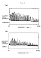
- Fig. 4 shows frequency characteristics of electric field strengths (noise spectra) of the printed boards according to the prior art and the present invention.
- the axis of abscissa represents frequency (Hz), while the axis of ordinate represents electric field strength (10dB/div.).
- (a) shows a frequency characteristic of the electric field strength of the conventional printed board without the magnetic prepreg 10
- (b) in Fig. 4 shows a frequency characteristic of the electric field strength of the printed board 20 using the magnetic prepreg 10 according to the present invention.
- the printed circuit boards formed with the same wiring patterns were used with respect to the prior art and the present invention.
- the electric field strengths are relatively lower with respect to the printed circuit board according to the present invention (Fig. 4 at (b)) as compared with the conventional printed circuit board (Fig. 4 at (a)). Specifically, it is appreciated that the printed circuit board according to the present invention can reduce the radiant noise.
- the printed circuit board excellent in noise characteristic can be obtained.
Landscapes
- Chemical & Material Sciences (AREA)
- Engineering & Computer Science (AREA)
- Materials Engineering (AREA)
- Microelectronics & Electronic Packaging (AREA)
- Manufacturing & Machinery (AREA)
- Health & Medical Sciences (AREA)
- Chemical Kinetics & Catalysis (AREA)
- Medicinal Chemistry (AREA)
- Polymers & Plastics (AREA)
- Organic Chemistry (AREA)
- Inorganic Chemistry (AREA)
- Physics & Mathematics (AREA)
- Electromagnetism (AREA)
- Composite Materials (AREA)
- Mechanical Engineering (AREA)
- Shielding Devices Or Components To Electric Or Magnetic Fields (AREA)
- Reinforced Plastic Materials (AREA)
- Production Of Multi-Layered Print Wiring Board (AREA)
- Soft Magnetic Materials (AREA)
- Laminated Bodies (AREA)
Abstract
Description
- The present invention relates to a printed circuit board and, in particular, to a printed circuit board which suppresses electromagnetic interference caused by interference of undesired electromagnetic waves.
- As is well known, a digital electronic device comprises a number of electronic components, such as a random access memory (RAM), a read-only memory (ROM), a microprocessor, and the like each of which comprises a number of logic elements. These electronic components are mounted on a printed circuit board having signal lines (wired conductors) wired around thereon. In recent digital electronic devices, the operation speed of the logic elements has been rapidly increased and further the reduction in weight, thickness, length and size of the device has also been highly advanced. Following this, the mounting density of the electronic components onto the printed circuit board has also been rapidly enhanced.
- However, since a signal flowing in the logic elements goes with abrupt changes in voltage and current, the electronic component is a noise generation source which generates high frequency noise. The high frequency noise causes interactions cooperatively with crosstalk noise or noise due to impedance mismatch so as to induce malfunctions relative to other electronic components on the printed circuit board and adversely affect other systems. Further, following the high-density mounting of the electronic components onto the printed circuit board and the reduction in size of the electronic components, electrostatic coupling between the electronic components and between the signal lines is increased so that the electromagnetic interference is liable to occur in the digital electronic device.
- Conventionally, in the general printed circuit board used in the digital electronic device, when operation frequency of signals flowing through the logic elements and the signal lines is low, electromagnetic coupling between the signal lines such as electromagnetic induction generated in the printed circuit board is relatively small so that no problem is raised. However, as the operation frequency of the signals flowing through the logic elements and the signal lines becomes high, the electromagnetic coupling between the signal lines is increased so that the foregoing problems are raised.
- Therefore, there has been proposed an electromagnetic wave shield circuit board of a structure in which the printed circuit board itself is provided with a shield layer, wherein undesired electromagnetic waves generated at the printed circuit board are screened by this electromagnetic wave shield layer. To be concrete, the foregoing electromagnetic wave shield circuit board has a structure wherein two circuit board surfaces are opposite to each other with the shield layer interposed therebetween. Here, the shield layer is formed of a conductor material which reflects the electromagnetic waves. Specifically, the screening of the electromagnetic waves by means of the shield layer aims to prevent invasion of the electromagnetic waves further inward therefrom by reflecting the electromagnetic waves incident thereupon. Accordingly, in the electromagnetic wave shield circuit board, a shield effect can be expected with respect to one circuit board surface confronting the opposite circuit board surface on the side where an electronic component to be a noise generation source is installed, while, with respect to the opposite circuit board surface on the side where the electronic component to be the noise generation source is installed, undesired radiation is generated due to the reflection of the electromagnetic waves is generated. As a result, there have been not a few cases wherein secondary electromagnetic coupling is promoted at the opposite circuit board surface on the side of the noise generation source. Further, in a floating digital electronic device, since the shield layer works as an antenna, secondary radiant noise is possibly generated from the shield layer.
- For solving such problems, in JP-A-8-46386 (hereinafter referred to as the prior art), the applicant of this application has offered a printed circuit board which does not spoil a shield effect of an electromagnetic wave shield circuit board and thus has a sufficient shield effect against transmittance of the electromagnetic waves, while, with respect to reflection of the electromagnetic waves, does not promote electromagnetic coupling at least due to reflection. In the printed circuit board disclosed in this prior art, a printed circuit base member having wired conductors on one side or both sides thereof comprises a conductive support and insulating soft magnetic layers provided on both sides of the conductive support. The insulating soft magnetic layer includes soft magnetic powder and an organic binding agent. Further, the insulating soft magnetic layer may have a dielectric layer on at least one side thereof. This dielectric layer includes dielectric powder and an organic binding agent. Alternatively, the foregoing insulating soft magnetic layer may include the soft magnetic powder, the dielectric powder and the organic binding agent. It is preferable that the foregoing soft magnetic powder is powder being flat and/or needle-shaped.
- On the other hand, a stacked body (electromagnetic interference suppressing layer) of the conductive support and the insulating soft magnetic body to be used in the foregoing printed circuit base member is produced, for example, in the following manner: Copper paste is formed into films on both sides of a polyimide film of 75µm by a doctor blade process to obtain a conductive support. Thereafter, soft magnetic paste is applied onto both sides of the conductive support by the doctor blade process to form insulating soft magnetic layers, which are then subjected to curing at 85°C for 24 hours to obtain a printed circuit base member.
- JP-A-02 120 040 also discloses a magnetic prepreg, a method of producing it and a printed circuit board using the magnetic prepreg.
- Conventionally, a prepreg constituting a printed circuit board is composed of resin and glass cloth. For example, the conventional prepreg is produced by impregnating thermosetting resin into a glass cloth and then drying and half-curing it.
- JP-A-02 087 593 discloses magnetic prepregs used for all
boards 11, 14 and 15. - Further, JP-A-08 186 378 discloses a prepreg 4a dipped with a magnetic material, and stacked to a side of a normal prepreg 3a, which itself is stacked via a wiring pattern 2 to a side of a plate or substrate 1.
- However, in the printed circuit board disclosed in the prior art document JP-A-08 46 386, there is a problem that it is difficult to form the insulating soft magnetic layers. On the other hand, since the conventional prepreg is constituted of only the resin and the glass cloth, the radiant noise can not be absorbed.
- Therefore, a theme of the present invention is to provide a magnetic prepreg which can absorb the radiant noise.
- Another theme of the present invention is to provide a method of producing the foregoing magnetic prepreg.
- Still another theme of the present invention is to provide a printed circuit board using the foregoing magnetic prepreg.
- For achieving the foregoing themes, according to a first aspect of the present invention, there is obtained a magnetic prepreg according to claim 1.
- According to a second aspect of the present invention, there is obtained a method of producing a magnetic prepreg acording to claim 3.
- According to a third aspect of the present invention, there is obtained a printed circuit board according to claim 4 using the foregoing magnetic prepreg.
-
- Fig. 1 is a sectional view showing a magnetic prepreg according to one embodiment of the present invention.
- Fig. 2 is a built-up sectional view showing a printed circuit board, using the magnetic prepreg shown in Fig. 1, in a disassembled state.
- Fig. 3 is a diagram showing production processes of the magnetic prepreg shown in Fig. 1 and the printed circuit board shown in Fig. 2.
- Fig. 4 is graphs showing frequency characteristics of electric field strengths with respect to printed circuit boards according to the prior art and the present invention, wherein (a) shows a frequency characteristic of the electric field strength of the conventional printed circuit board and (b) shows a frequency characteristic of the electric field strength of the printed circuit board according to the present invention.
-
- Now, the present invention will be explained in detail with reference to the drawings.
- Referring to Fig. 1, a
magnetic prepreg 10 according to one embodiment of the present invention is formed by impregnating amagnetic paint 12 composed of soft magnetic powder 121 andthermosetting resin 122 into aglass cloth 14. It is preferable that the soft magnetic powder 121 is metal powder being substantially flat. Further, it is preferable that a main component of thethermosetting resin 122 is epoxy resin. - As the thermosetting resin 122, (poly) urethane resin, phenol resin, amide resin, imide resin or the like can be cited other than the epoxy resin. As the soft
magnetic powder 12, an Fe-Al-Si alloy (this is called Sendust (trademark)) or an Fe-Ni alloy (Permalloy) having a large high frequency permeability can be cited as a typical material thereof. The softmagnetic powder 12 is used by being finely powdered and by oxidizing surface portions thereof. It is preferable that an aspect ratio of the softmagnetic powder 12 is sufficiently large (for example, approximately not less than 5 : 1). By rendering substantially flat the shape of the softmagnetic powder 12, undesired radiant noise can be absorbed and suppressed more efficiently. This is because if the softmagnetic powder 12 is essentially flat in shape and oriented/aligned in an in-surface direction in the magnetic prepreg, a shape anisotropy appears so that a complex permeability based on a magnetic resonance is increased at a high frequency region. - As the foregoing
magnetic paint 12, one shown in Table 1 below can be used.Flat soft magnetic fine powder 90 weight parts Composition: Fe-Al-Si alloy Mean particle diameter: 30µm Aspect ratio: about 10 Thermosetting resin Brominated epoxy resin 15 weight parts O-cresol novolak type epoxy resin 5 weight parts Dicyandiamide 0.8 weight parts Dimethyl benzylamine 0.06 weight parts Solvent Mixture of MEK, DMF and methyl cellosolve 40 weight parts - Fig. 2 shows a printed
circuit board 20 using themagnetic prepreg 10 shown in Fig. 1. The shown printedcircuit board 20 is formed by sandwiching aninternal layer member 22 being a normal prepreg composed of resin and glass cloth, with a pair of themagnetic prepregs 10 from both sides thereof viacopper foils 24, and covering the exposed surfaces of themagnetic prepregs 10 withcopper foils 24. Thecopper foils 24 each have a thickness of, for example, about 0.035mm and are formed with a wiring pattern. Theinternal layer member 22 and themagnetic prepregs 10 are formed with through holes, not shown, and the copper foils (wiring patterns) 24 are electrically connected to each other via the through holes. - Now, referring to Fig. 3, a method of producing the
magnetic prepreg 10 and the printedcircuit board 20 will be explained. - First, as shown in Fig. 3 at (a), a web-
like glass cloth 14 is passed through the inside of avessel 30 containing themagnetic paint 12 so as to be impregnated with themagnetic paint 12 of a necessary amount. It is preferable to carry out a magnetic alignment procedure by means of, such as passing theglass cloth 14, after having been impregnated with themagnetic paint 12, through a solenoid magnet (not shown). - Subsequently, as shown in Fig. 3 at (b), the
glass cloth 14 impregnated with themagnetic paint 12 is passed through a drier 40 whose temperature is uniformly controlled, so as to advance a resin reaction. After the drying, as shown in Fig. 3 at (c), it is cut to required dimensions. The cut one is called aresin cloth 50. In this manner, the magnetic prepreg 10 (Fig. 1) is produced. - Subsequently, as shown in Fig. 3 at (d), a fixed number of the
resin cloths 50, the internal layer member 22 (Fig. 2) and the copper foils 24 are combined and applied with a stainless plate (not shown). Then, as shown in Fig. 3 at (e), the material applied with the stainless plate is subjected to press/formation in amultistage press machine 60. In this manner, the printed circuit board 20 (Fig. 2) is produced. - Fig. 4 shows frequency characteristics of electric field strengths (noise spectra) of the printed boards according to the prior art and the present invention. In Fig. 4, the axis of abscissa represents frequency (Hz), while the axis of ordinate represents electric field strength (10dB/div.). In Fig. 4, (a) shows a frequency characteristic of the electric field strength of the conventional printed board without the
magnetic prepreg 10, while (b) in Fig. 4 shows a frequency characteristic of the electric field strength of the printedboard 20 using themagnetic prepreg 10 according to the present invention. The printed circuit boards formed with the same wiring patterns were used with respect to the prior art and the present invention. - As evident from Fig. 4, the electric field strengths are relatively lower with respect to the printed circuit board according to the present invention (Fig. 4 at (b)) as compared with the conventional printed circuit board (Fig. 4 at (a)). Specifically, it is appreciated that the printed circuit board according to the present invention can reduce the radiant noise.
- While the present invention has been explained by citing some embodiments, it is needless to say that the present invention is not limited to the foregoing embodiments, but can be modified in various ways without departing from the scope of the present invention as defined by the appended claims. For example, it is a matter of course that the materials of the soft magnetic powder or the thermosetting resin are not limited to those of the embodiments. Further, it is a matter of course that the number of the stacked layers of the magnetic prepreg constituting the printed circuit board is not limited to that of the embodiments.
- As described above, according to the present invention, by using the magnetic prepreg formed by impregnating the magnetic paint composed of the soft magnetic powder and the thermosetting resin into the glass cloth, the printed circuit board excellent in noise characteristic can be obtained.
Claims (4)
- A magnetic prepreg formed by impregnating a magnetic paint composed of soft magnetic metal powder being essentially flat in shape and thermosetting resin into a glass cloth, wherein said soft magnetic metal powder is oriented/aligned in an in-surface direction of the magnetic prepreg by a magnetic alignment procedure.
- The magnetic prepreg as recited in claim 1, characterized in that a main component of said thermosetting resin is epoxy resin.
- A method of producing a magnetic prepreg characterized in that a magnetic paint composed of soft magnetic metal powder being essentially flat in shape and thermosetting resin is impregnated into a glass cloth, then dried and further cured into a half-cured state, after that a magnetic alignment procedure is carried out in an in-surface direction of said magnetic prepreg.
- A printed circuit board using the magnetic prepreg as recited in claim 1 or 2, said printed circuit board comprising a normal prepreg composed of resin and glass cloth and at least one of said magnetic prepregs according to claim 1 or 2 stacked to at least one side of said normal prepreg via a wiring pattern.
Applications Claiming Priority (4)
| Application Number | Priority Date | Filing Date | Title |
|---|---|---|---|
| JP235299/96 | 1996-09-05 | ||
| JP8235299A JPH1079593A (en) | 1996-09-05 | 1996-09-05 | Magnetic prepreg, method of manufacturing the same, and printed wiring board using the same |
| JP23529996 | 1996-09-05 | ||
| PCT/JP1997/003101 WO1998010626A1 (en) | 1996-09-05 | 1997-09-04 | Magnetic prepreg, its manufacturing method and printed wiring board employing the prepreg |
Publications (3)
| Publication Number | Publication Date |
|---|---|
| EP0878984A1 EP0878984A1 (en) | 1998-11-18 |
| EP0878984A4 EP0878984A4 (en) | 2000-08-16 |
| EP0878984B1 true EP0878984B1 (en) | 2004-11-24 |
Family
ID=16984066
Family Applications (1)
| Application Number | Title | Priority Date | Filing Date |
|---|---|---|---|
| EP97939168A Expired - Lifetime EP0878984B1 (en) | 1996-09-05 | 1997-09-04 | Magnetic prepreg, its manufacturing method and printed wiring board employing the prepreg |
Country Status (8)
| Country | Link |
|---|---|
| US (1) | US6362434B1 (en) |
| EP (1) | EP0878984B1 (en) |
| JP (1) | JPH1079593A (en) |
| KR (1) | KR100451454B1 (en) |
| CN (1) | CN1089543C (en) |
| DE (1) | DE69731730T2 (en) |
| TW (1) | TW346710B (en) |
| WO (1) | WO1998010626A1 (en) |
Cited By (2)
| Publication number | Priority date | Publication date | Assignee | Title |
|---|---|---|---|---|
| CN105121576A (en) * | 2013-03-28 | 2015-12-02 | 日东电工株式会社 | Soft magnetic thermosetting adhesive film, magnetic-film-laminated circuit board, and position detection device |
| US12543267B2 (en) | 2021-05-18 | 2026-02-03 | At&S Austria Technologie & Systemtechnik Aktiengesellschaft | Magnetic inlay with an adjustable inductance value for a component carrier and a manufacturing method |
Families Citing this family (24)
| Publication number | Priority date | Publication date | Assignee | Title |
|---|---|---|---|---|
| US6908960B2 (en) * | 1999-12-28 | 2005-06-21 | Tdk Corporation | Composite dielectric material, composite dielectric substrate, prepreg, coated metal foil, molded sheet, composite magnetic substrate, substrate, double side metal foil-clad substrate, flame retardant substrate, polyvinylbenzyl ether resin composition, thermosettin |
| KR100533097B1 (en) | 2000-04-27 | 2005-12-02 | 티디케이가부시기가이샤 | Composite Magnetic Material and Magnetic Molding Material, Magnetic Powder Compression Molding Material, and Magnetic Paint using the Composite Magnetic Material, Composite Dielectric Material and Molding Material, Powder Compression Molding Material, Paint, Prepreg, and Substrate using the Composite Dielectric Material, and Electronic Part |
| CN1218333C (en) * | 2000-12-28 | 2005-09-07 | Tdk株式会社 | Laminated circuit board and prodroduction method for electronic part, and laminated electronic part |
| WO2003107729A1 (en) * | 2002-06-14 | 2003-12-24 | Laird Technologies, Inc. | Composite emi shield |
| US6764732B2 (en) * | 2002-07-11 | 2004-07-20 | Magna Paper Llc | Adhesive magnet receptive media |
| KR100463593B1 (en) * | 2002-11-27 | 2004-12-29 | 주식회사 메틱스 | Electro magnetic absorption sheet and manufacturing method of electro magnetic absorption sheet |
| US7449241B2 (en) * | 2003-08-04 | 2008-11-11 | General Electric Company | Organic coating compositions for aluminizing metal substrates, and related methods and articles |
| US7332024B2 (en) * | 2004-04-29 | 2008-02-19 | General Electric Company | Aluminizing composition and method for application within internal passages |
| EP1768471B1 (en) * | 2004-06-23 | 2013-05-29 | Hitachi Chemical Co., Ltd. | Prepreg for printed wiring board, metal foil clad laminate and printed wiring board, and, method for manufacturing multi-layer printed wiring board |
| JP3972951B2 (en) * | 2005-07-04 | 2007-09-05 | オムロン株式会社 | Switching power supply, power supply device and electronic equipment |
| WO2007040064A1 (en) * | 2005-09-30 | 2007-04-12 | Matsushita Electric Industrial Co., Ltd. | Sheet-like composite electronic component and method for manufacturing same |
| JP4818852B2 (en) * | 2006-08-31 | 2011-11-16 | ソニーケミカル&インフォメーションデバイス株式会社 | Magnetic sheet manufacturing method and magnetic sheet |
| JP5139750B2 (en) * | 2006-11-22 | 2013-02-06 | Necトーキン株式会社 | Multilayer printed circuit board |
| JP4980322B2 (en) * | 2008-09-17 | 2012-07-18 | アルプス電気株式会社 | Multilayer wiring board and manufacturing method thereof |
| CN101604568B (en) * | 2009-04-30 | 2012-09-05 | 兰州大学 | Magnetic field oriented flaky soft magnetic composite material and preparation method thereof |
| GB201110233D0 (en) * | 2011-06-16 | 2011-08-03 | Williams Hybrid Power Ltd | Magnetically loaded composite rotors and tapes used in the production thereof |
| DE102011087263A1 (en) * | 2011-11-28 | 2013-05-29 | Lenze Drives Gmbh | Screening device for electric appliance, has shielding conductive plate with electrically conductive inner layers that is arranged between noise-sensitive unit and line reactor |
| GB2509753A (en) * | 2013-01-14 | 2014-07-16 | Bae Systems Plc | Ferrite Fibre Composites |
| KR20150007766A (en) * | 2013-07-12 | 2015-01-21 | 삼성전기주식회사 | Inductor and method for manufacturing the same |
| DE102014210013A1 (en) | 2014-05-26 | 2015-11-26 | Schaeffler Technologies AG & Co. KG | Magnetic board and method for its manufacture |
| PL3849767T3 (en) * | 2018-09-12 | 2026-08-10 | Composecure Llc | Metal-doped epoxy resin transaction card and process for manufacture |
| CN113906528B (en) | 2019-05-15 | 2026-02-13 | 3M创新有限公司 | Orientation of magnetic fillers for optimizing membrane properties |
| CN115915593A (en) * | 2021-09-30 | 2023-04-04 | 华为技术有限公司 | A printed circuit board, power supply, inductor, transformer and electronic equipment |
| KR20240114212A (en) * | 2023-01-16 | 2024-07-23 | 삼성에스디아이 주식회사 | Rechargeable battery module |
Family Cites Families (14)
| Publication number | Priority date | Publication date | Assignee | Title |
|---|---|---|---|---|
| DE1940039A1 (en) * | 1969-08-06 | 1971-02-18 | Siemens Ag | Circuit board |
| US4092459A (en) * | 1975-01-13 | 1978-05-30 | Graham Magnetics Incorporated | Powder products |
| JPS5557212A (en) * | 1978-10-24 | 1980-04-26 | Fujitsu Ltd | High dielectric laminate plate |
| US4496415A (en) * | 1982-04-08 | 1985-01-29 | Westinghouse Electric Corp. | Method for impregnating resin powder directly into a laminate lay up |
| JPS59187160U (en) * | 1983-05-31 | 1984-12-12 | ティーディーケイ株式会社 | Printed board |
| JPH0287593A (en) * | 1988-09-24 | 1990-03-28 | Mitsubishi Electric Corp | Printed wiring board |
| JPH02120040A (en) * | 1988-10-28 | 1990-05-08 | Hitachi Chem Co Ltd | Electric wave absorbing copper clad laminate |
| US5207841A (en) * | 1990-04-12 | 1993-05-04 | Tdk Corporation | Soft magnetic powder and magnetic shield composition |
| JPH0595197A (en) * | 1991-10-01 | 1993-04-16 | Mitsui Toatsu Chem Inc | Printed wiring board and substrate used therefor |
| JPH0621595A (en) * | 1992-07-03 | 1994-01-28 | Cmk Corp | Material for printed wiring board |
| JP3224936B2 (en) * | 1994-03-03 | 2001-11-05 | 日本シイエムケイ株式会社 | Printed wiring board material containing magnetic material in insulating layer |
| JP3528257B2 (en) * | 1994-07-29 | 2004-05-17 | Necトーキン株式会社 | Printed wiring board |
| DE4441436A1 (en) * | 1994-11-23 | 1996-05-30 | Vdo Schindling | Carrier substrate for electronic components or circuits e.g. for motor vehicles electronic equipment |
| JPH08186378A (en) * | 1994-12-29 | 1996-07-16 | Cmk Corp | Multilayer printed wiring board having magnetic material and manufacturing method thereof |
-
1996
- 1996-09-05 JP JP8235299A patent/JPH1079593A/en active Pending
-
1997
- 1997-09-04 KR KR10-1998-0703165A patent/KR100451454B1/en not_active Expired - Fee Related
- 1997-09-04 WO PCT/JP1997/003101 patent/WO1998010626A1/en not_active Ceased
- 1997-09-04 US US09/066,381 patent/US6362434B1/en not_active Expired - Lifetime
- 1997-09-04 CN CN97191174A patent/CN1089543C/en not_active Expired - Fee Related
- 1997-09-04 EP EP97939168A patent/EP0878984B1/en not_active Expired - Lifetime
- 1997-09-04 DE DE69731730T patent/DE69731730T2/en not_active Expired - Lifetime
- 1997-09-05 TW TW086112814A patent/TW346710B/en not_active IP Right Cessation
Cited By (4)
| Publication number | Priority date | Publication date | Assignee | Title |
|---|---|---|---|---|
| CN105121576A (en) * | 2013-03-28 | 2015-12-02 | 日东电工株式会社 | Soft magnetic thermosetting adhesive film, magnetic-film-laminated circuit board, and position detection device |
| EP2980174A4 (en) * | 2013-03-28 | 2016-11-09 | Nitto Denko Corp | SOFT MAGNETIC THERMAL HARDENING FILM, COATED PLATE AND POSITION DETECTION DEVICE FILMED WITH THE SOFT MAGNETIC FOIL |
| CN105121576B (en) * | 2013-03-28 | 2018-05-29 | 日东电工株式会社 | Soft magnetism Thermocurable adhering film, thin magnetic film are stacked circuit substrate and position detecting device |
| US12543267B2 (en) | 2021-05-18 | 2026-02-03 | At&S Austria Technologie & Systemtechnik Aktiengesellschaft | Magnetic inlay with an adjustable inductance value for a component carrier and a manufacturing method |
Also Published As
| Publication number | Publication date |
|---|---|
| WO1998010626A1 (en) | 1998-03-12 |
| EP0878984A4 (en) | 2000-08-16 |
| JPH1079593A (en) | 1998-03-24 |
| DE69731730T2 (en) | 2005-11-03 |
| CN1089543C (en) | 2002-08-21 |
| US6362434B1 (en) | 2002-03-26 |
| CN1199538A (en) | 1998-11-18 |
| KR20000064305A (en) | 2000-11-06 |
| KR100451454B1 (en) | 2004-12-17 |
| TW346710B (en) | 1998-12-01 |
| EP0878984A1 (en) | 1998-11-18 |
| DE69731730D1 (en) | 2004-12-30 |
Similar Documents
| Publication | Publication Date | Title |
|---|---|---|
| US6362434B1 (en) | Magnetic prepreg, its manufacturing method and printed wiring board employing the prepreg | |
| EP0785557B1 (en) | Composite magnetic material and product for eliminating electromagnetic interference | |
| JP3401650B2 (en) | Electromagnetic interference suppressor | |
| EP0667643B1 (en) | Electromagnetic interference suppressing body having low electromagnetic transparency and reflection, and electronic equipment having the same | |
| US7888599B2 (en) | Printed circuit board including embedded capacitor and method of fabricating same | |
| EP0633715B1 (en) | Printed circuit board | |
| US6310285B1 (en) | EMI preventive part and active device with the same | |
| JPH05191056A (en) | Printed wiring board | |
| JPH09116289A (en) | Noise suppression electronic device and method of manufacturing the same | |
| JPH1084195A5 (en) | ||
| JP2000173824A (en) | Electronic components | |
| JPH02120040A (en) | Electric wave absorbing copper clad laminate | |
| JP3528257B2 (en) | Printed wiring board | |
| JPH08204380A (en) | Noise suppression method in electronic device and noise suppression type electronic device applying the same | |
| JPH1154861A (en) | Wiring board | |
| JPH07212043A (en) | Printed wiring board and multi-wire wiring board | |
| JPH0682890B2 (en) | EMI countermeasure circuit board and method of manufacturing the same | |
| JPH0766587A (en) | Printed wiring board having magnetic coating film and electromagnetic wave shield layer and method for manufacturing the same | |
| JPH0287593A (en) | Printed wiring board | |
| KR100636826B1 (en) | Noise reduction flexible film and electromagnetic wave shielding circuit board including the same | |
| JP3505691B2 (en) | Electronic equipment | |
| JPH0758487A (en) | Printed wiring board having magnetic coating film and electromagnetic wave shield layer and method for manufacturing the same | |
| AU648943B2 (en) | Printed circuit board | |
| JPH05291806A (en) | Printed circuit board for high frequency | |
| JP2724351B2 (en) | Manufacturing method of radio wave shielding printed wiring board |
Legal Events
| Date | Code | Title | Description |
|---|---|---|---|
| PUAI | Public reference made under article 153(3) epc to a published international application that has entered the european phase |
Free format text: ORIGINAL CODE: 0009012 |
|
| 17P | Request for examination filed |
Effective date: 19980428 |
|
| AK | Designated contracting states |
Kind code of ref document: A1 Designated state(s): DE FR GB IT |
|
| A4 | Supplementary search report drawn up and despatched |
Effective date: 20000703 |
|
| AK | Designated contracting states |
Kind code of ref document: A4 Designated state(s): DE FR GB IT |
|
| RAP1 | Party data changed (applicant data changed or rights of an application transferred) |
Owner name: NEC TOKIN CORPORATION |
|
| 17Q | First examination report despatched |
Effective date: 20030903 |
|
| GRAP | Despatch of communication of intention to grant a patent |
Free format text: ORIGINAL CODE: EPIDOSNIGR1 |
|
| GRAS | Grant fee paid |
Free format text: ORIGINAL CODE: EPIDOSNIGR3 |
|
| RIN1 | Information on inventor provided before grant (corrected) |
Inventor name: KAMEI, KOJI,NEC TOKIN CORPORATION Inventor name: SATO, MITSUHARU,NEC TOKIN CORPORATION Inventor name: YOSHIDA, SHIGEYOSHI,NEC TOKIN CORPORATION |
|
| GRAA | (expected) grant |
Free format text: ORIGINAL CODE: 0009210 |
|
| AK | Designated contracting states |
Kind code of ref document: B1 Designated state(s): DE FR GB IT |
|
| REG | Reference to a national code |
Ref country code: GB Ref legal event code: FG4D |
|
| REF | Corresponds to: |
Ref document number: 69731730 Country of ref document: DE Date of ref document: 20041230 Kind code of ref document: P |
|
| PG25 | Lapsed in a contracting state [announced via postgrant information from national office to epo] |
Ref country code: IT Free format text: LAPSE BECAUSE OF NON-PAYMENT OF DUE FEES;WARNING: LAPSES OF ITALIAN PATENTS WITH EFFECTIVE DATE BEFORE 2007 MAY HAVE OCCURRED AT ANY TIME BEFORE 2007. THE CORRECT EFFECTIVE DATE MAY BE DIFFERENT FROM THE ONE RECORDED. Effective date: 20050904 |
|
| PLBE | No opposition filed within time limit |
Free format text: ORIGINAL CODE: 0009261 |
|
| STAA | Information on the status of an ep patent application or granted ep patent |
Free format text: STATUS: NO OPPOSITION FILED WITHIN TIME LIMIT |
|
| ET | Fr: translation filed | ||
| 26N | No opposition filed |
Effective date: 20050825 |
|
| PGFP | Annual fee paid to national office [announced via postgrant information from national office to epo] |
Ref country code: GB Payment date: 20090902 Year of fee payment: 13 |
|
| PGFP | Annual fee paid to national office [announced via postgrant information from national office to epo] |
Ref country code: FR Payment date: 20100921 Year of fee payment: 14 |
|
| PGFP | Annual fee paid to national office [announced via postgrant information from national office to epo] |
Ref country code: DE Payment date: 20100901 Year of fee payment: 14 |
|
| GBPC | Gb: european patent ceased through non-payment of renewal fee |
Effective date: 20100904 |
|
| PG25 | Lapsed in a contracting state [announced via postgrant information from national office to epo] |
Ref country code: GB Free format text: LAPSE BECAUSE OF NON-PAYMENT OF DUE FEES Effective date: 20100904 |
|
| REG | Reference to a national code |
Ref country code: FR Ref legal event code: ST Effective date: 20120531 |
|
| PG25 | Lapsed in a contracting state [announced via postgrant information from national office to epo] |
Ref country code: DE Free format text: LAPSE BECAUSE OF NON-PAYMENT OF DUE FEES Effective date: 20120403 |
|
| REG | Reference to a national code |
Ref country code: DE Ref legal event code: R119 Ref document number: 69731730 Country of ref document: DE Effective date: 20120403 |
|
| PG25 | Lapsed in a contracting state [announced via postgrant information from national office to epo] |
Ref country code: FR Free format text: LAPSE BECAUSE OF NON-PAYMENT OF DUE FEES Effective date: 20110930 |