TECHNICAL FIELD
The present invention relates to a transmitter-receiver
circuit and also relates to a semiconductor integrated circuit
device including the transmitter-receiver circuit. More
particularly, the present invention relates to transmitter-receiver
circuit and semiconductor integrated circuit device
suitable for a wireless communication unit using the same
frequency as both transmission frequency and reception frequency.
BACKGROUND ART
In recent years, size, weight and price of various wireless
communication units, e.g., portable cellular phone units
for radio communication, have been drastically reduced, and
the number of users thereof has been rapidly increasing. In
conventional communication systems, a system configuration
requiring distinct frequencies for transmission and reception
has been adopted so far. On the other hand, in order to satisfy
the needs of an even larger number of users, digital implementation
has been gradually applied to these units.
While two distinct frequencies per line have been required
conventionally, such a digital wireless communication unit
can perform transmission and reception with the same frequency
by dividing transmission and reception in a time-division
manner.
Even in such a wireless communication unit utilizing
digital implementation, however, various circuits in a wireless
circuit section, including a transmitter amplifier, a
low-noise receiver amplifier and a transmission/reception
mode switch for switching transmission and reception, are
still implemented by conventional circuits. Thus, it is an
important problem to develop downsized transmitter-receiver
circuits and, in particular, semiconductor integrated circuit
integrated with these circuits that are suitably applicable
to brand-new digital implementation.
Also, a circuit including gallium-arsenide field effect
transistors (hereinafter, simply referred to as "GaAs FETs"),
having low-voltage, high-efficiency and low-noise operating
characteristics and high-isolation characteristics, are often
used for a transmitter amplifier, a low-noise receiver amplifier
and a transmission/reception mode switch in a transmitter-receiver
circuit for a wireless communication unit of a
digital type.
Hereinafter, an example of a conventional transmitter-receiver
circuit will be described with reference to the
drawings.
Figure 11 illustrates a configuration of a conventional
digital transmitter-receiver circuit using FETs. In Figure 11,
110 denotes a transmitter amplifier for amplifying an input
signal to be transmitted and then outputting the amplified
signal. 120 denotes a low-noise receiver amplifier for amplifying
an input received signal and then outputting the amplified
signal. 130 denotes a mode switch for switching
transmission state and reception state in a time-division manner.
140 denotes a first matching circuit for matching the
impedance of the input received signal with the input impedance
of the low-noise receiver amplifier 120. 150 denotes a
second matching circuit for matching the output impedance of
the transmitter amplifier 110 with predetermined impedance.
160 denotes a third matching circuit for matching the output
impedance of a FET 112 on the first stage with the input impedance
of a FET on the second stage. 171 denotes first coupling
capacitance for ac coupling the transmitter amplifier
110 with the second matching circuit 150. 172 denotes second
coupling capacitance for ac coupling the mode switch 130 with
the first matching circuit 140. 173 denotes a first interconnection,
having characteristic impedance of 50Ω, for connecting
the mode switch 130 to the second matching circuit 150.
174 denotes a second interconnection, having characteristic
impedance of 50Ω, for connecting the mode switch 130 to the
first matching circuit 140. 175 denotes a third interconnection,
having characteristic impedance of 50Ω, for connecting
the mode switch 130 to an antenna 180 used both for transmission
and reception.
In the transmitter amplifier 110 shown in Figure 11, 111
denotes an input terminal, through which a signal to be
transmitted is input. 112 denotes a FET on the first stage,
of which the gate electrode is provided with the input signal
to be transmitted and the source is grounded. 113 denotes a
first power supply terminal connected to the drain electrode
of the FET 112 on the first stage. 114 denotes a FET on the
second stage, of which the gate electrode is provided with
the signal to be transmitted via the third matching circuit
160 and the source is grounded. 115 denotes a second power
supply terminal connected to the drain electrode of the FET
114 on the second stage. 116 denotes an output terminal connected
to the drain electrode of the FET 114 on the second
stage.
In the low-noise receiver amplifier 120 shown in Figure
11, 121 denotes an input terminal, through which a received
signal is input via the first matching circuit 140. 122 denotes
a low-noise FET, of which the gate electrode is provided
with the received signal and the source is grounded. 123
denotes an output terminal connected to the drain electrode
of the low-noise FET 122.
In the mode switch 130 shown in Figure 11, 131 denotes
an input terminal on the transmission side connected to the
second matching circuit 150. 132 denotes an input/output
terminal on the antenna side for outputting a signal to be
transmitted, which has been amplified by the transmitter amplifier
110 and then input thereto via the second matching
circuit 150 during transmission, to the antenna 180, and for
receiving the received signal that has been received by the
antenna 180 during reception. 133 denotes an output terminal
on the reception side, through which the received signal input
from the input/output terminal 132 on the antenna side is
output. 134A denotes first switch-control-signal input terminals
for controlling a first switching FET 135 and a third
switching FET 137. 134B denotes second switch-control-signal
input terminals for controlling a second switching FET 136
and a fourth switching FET 138.
In the first matching circuit 140 shown in Figure 11,
141 denotes an input terminal connected to the output terminal
133 on the reception side of the mode switch 130 via the
second coupling capacitance 172. 142 denotes an output terminal
connected to the input terminal 121 of the low-noise
receiver amplifier 120. 143 denotes a first inductor, one
end of which is connected to the input terminal 141 and the
other end of which is grounded, for constituting the first
matching circuit 140. 144 denotes a second inductor, one end
of which is connected to the input terminal 141 and the other
end of which is connected to the output terminal 142, for
constituting the first matching circuit 140.
In the second matching circuit 150 shown in Figure 11,
151 denotes an input terminal connected to the output terminal
116 of the transmitter amplifier via the first coupling
capacitance 171. 152 denotes an output terminal connected to
the input terminal 131 on the transmission side of the mode
switch 130. 153 denotes a first capacitor, one end of which
is connected to the input terminal 151 and the other end of
which is grounded, for constituting the second matching circuit
150. 154 denotes an inductor, one end of which is connected
to the input terminal 151 and the other end of which
is connected to a second capacitor 155, for constituting the
second matching circuit 150. 155 denotes the second capacitor,
one end of which is connected to the inductor 154 and
the other end of which is connected to the output terminal
152, for constituting the second matching circuit 150.
In the third matching circuit 160 shown in Figure 11,
161 denotes a first capacitor, one end of which is connected
to the drain electrode of the FET 112 on the first stage in
the transmitter amplifier 110 and the other end of which is
connected to an inductor 162, for constituting the third
matching circuit 160. 162 denotes the inductor, one end of
which is connected to the first capacitor 161 and the other
end of which is connected to the gate electrode of the FET
114 on the second stage in the transmitter amplifier 110, for
constituting the third matching circuit 160. 163 denotes a
second capacitor, one end of which is connected to the inductor
162 and the gate electrode of the FET 114 on the second
stage and the other end of which is grounded, for constituting
the third matching circuit 160.
Hereinafter, the operation of the transmitter-receiver
circuit having the above-described configuration will be described.
First, the operation during reception will be described.
A less intense received signal, input via the antenna
180, passes through the third interconnection 175 having
characteristic impedance of 50 Ω and is input to the input/output
terminal 132 on the antenna side of the mode
switch 130. At this point in time, in the mode switch 130,
the first switching FET 135 and the third switching FET 137
have been turned ON responsive to the control signal input
through the first switch-control-signal input terminals 134A,
while the second switching FET 136 and the fourth switching
FET 138 have been turned OFF responsive to the control signal
input through the second switch-control-signal input terminals
134B. Thus, the input signal is selectively directed to the
low-noise receiver amplifier 120 via the third switching FET
137, which has been turned ON. On the other hand, the circuit
section including the transmitter amplifier 110 is electrically
isolated from the circuit section including the low-noise
receiver amplifier 120, because the second switching FET 136
has been turned OFF. Also, the former circuit section is
short-circuited, because the first switching FET 135 has been
turned ON.
The signal switched by the third switching FET 137 in
the conductive state is output through the output terminal on
the reception side of the mode switch 130, passed through the
second interconnection 174 having characteristic impedance of
50 Ω and the second coupling capacitance 172 and then input
to the first matching circuit 140. Then, impedance matching
is performed by the first inductor 143 and the second inductor
144 of the first matching circuit 140. Thereafter, the
signal is input to the input terminal 121 of the low-noise
receiver amplifier 120. The received signal input to the
low-noise receiver amplifier 120 is amplified by the low-noise
FET 122 and the amplified signal is output through the
output terminal 123.
Next, the operation during transmission will be described.
First, modulated signal to be transmitted is input to
the input terminal 111 of the transmitter amplifier 110. Power
amplification on the first stage is performed by the FET
112 on the first stage. Impedance conversion is performed by
the third matching circuit 160. Then, the signal is input to
the FET 114 on the second stage. The power of the signal is
amplified by the FET 114 on the second stage so as to reach
predetermined power. The amplified signal to be transmitted
is input to the second matching circuit 150 via the first
coupling capacitance 171. The characteristic impedance thereof
is converted to be 50Ω. And then the signal is input to
the input terminal 131 on the transmission side of the mode
switch 130 through the first interconnection 173 having characteristic
impedance of 50Ω.
At this point in time, in the mode switch 130, the second
switching FET 136 and the fourth switching FET 138 have
been turned ON responsive to the control signal input through
the second switch-control-signal input terminals 134B, while
the first switching FET 135 and the third switching FET 137
have been turned OFF responsive to the control signal input
through the first switch-control-signal input terminals 134A.
Thus, the input signal to be transmitted is selectively directed
to the antenna 180 via the second switching FET 136,
which has been turned ON. On the other hand, the circuit section
including the low-noise receiver amplifier 120 is electrically
isolated from the circuit section including the
transmitter amplifier 110, because the third switching FET 137
has been turned OFF. Also, the former circuit section is
short-circuited, because the fourth switching FET 138 has been
turned ON.
The amplified signal to be transmitted passes through
the second switching FET 136 in the conductive state and the
third interconnection 175 having characteristic impedance of
50 Ω and is input to the antenna 180 so as to be output
through the antenna 180 as radio waves.
The above-described conventional transmitter-receiver
circuit, however, had a problem in that the loss of a signal
passing through the mode switch 130 is large. In particular,
the loss of a signal to be transmitted becomes an issue because
such a signal requires high power. Thus, it is necessary
to improve the performance of a through switching FET on
the transmission side. In general, in order to reduce the
pass loss, a switching FET having a large gate length is required.
In addition, if switching FETs of such a large size
are integrated, then the chip area is increased to such a degree
that the area occupied by the mode switch 130 becomes
substantially equal to the area of the transmitter amplifier
110. Thus, problems are present in that downsizing and costreduction
thereof are hard to realize.
The present invention can solve the above-described conventional
problems all at once, and has objects of reducing
the power consumption by eliminating the pass loss caused by
the mode switch on the signal to be transmitted and downsizing
a wireless communication unit by reducing the area occupied
by the mode switch in the transmitter-receiver circuit.
DISCLOSURE OF THE INVENTION
In order to accomplish the above-described objects, the
present invention connects a transmitter amplifier to an antenna
without interposing any mode switch therebetween by
matching the inputs to a receiver amplifier while using, in
combination, the output impedance of the transmitter amplifier
during the OFF state and the output impedance to the receiver
amplifier.
A transmitter-receiver circuit for a wireless communication
unit according to the present invention includes: a
transmitter amplifier for amplifying and outputting an input
signal to be transmitted; a receiver amplifier for amplifying
and outputting an input received signal; and a mode switch,
connected to an antenna used for both transmission and reception,
for switching a transmission state where the signal to
be transmitted, which has been output by the transmitter amplifier,
is output to the antenna and a reception state where
the received signal, to be input to the receiver amplifier,
is input through the antenna. The transmitter amplifier includes:
an amplifying FET, having a gate electrode connected
to an input terminal of the signal to be transmitted, a drain
electrode connected to a power supply terminal and a source
electrode grounded; a matching circuit, connected between the
drain electrode of the FET and the antenna, for matching output
impedance of the FET with impedance on the antenna side; a
control terminal connected to the gate electrode of the FET;
and an output terminal directly connected to the antenna
without passing through the mode switch.
In the transmitter-receiver circuit for a wireless communication
unit, since the output terminal of the transmitter
amplifier is directly connected to the antenna without passing
through the mode switch during transmission, the pass
loss, ordinarily caused by a switch on a signal to be transmitted,
can be eliminated. As a result, the power consumption
can be reduced. On the other hand, during reception, since a
control terminal connected to the gate electrode of the FET of
the transmitter amplifier is provided, the circuit section on
the transmission side is short-circuited by applying a predetermined
voltage to the gate electrode and using the FET having
the grounded source as resistance. As a result, a mode
switch on the transmission side, which has conventionally been
required, is no longer necessary. In other words, a mode
switch on the reception side may be constituted by only one
switching device, and thus the area occupied by the mode
switch in the entire circuit can be reduced. As a result, the
overall size of the transmitter-receiver circuit can be reduced.
Another transmitter-receiver circuit for a wireless communication
unit according to the present invention includes:
a transmitter amplifier for amplifying and outputting an input
signal to be transmitted; a receiver amplifier for amplifying
and outputting an input received signal; and a mode
switch, connected to an antenna used for both transmission
and reception, for switching a transmission state where the
signal to be transmitted, which has been output by the transmitter
amplifier, is output to the antenna and a reception
state where the received signal, to be input to the receiver
amplifier, is input through the antenna. The transmitter amplifier
includes: an amplifying FET, having a gate electrode
connected to an input terminal of the signal to be transmitted,
a drain electrode connected to a power supply terminal
and a source electrode grounded; a matching circuit, connected
between the drain electrode of the FET and the antenna, for
matching output impedance of the FET with impedance on the antenna
side; a control terminal connected to the gate electrode
of the FET; and an output terminal directly connected to
the antenna without passing through the mode switch. The input
terminal on the antenna side of the mode switch is connected
to a terminal of the matching circuit, which is
different from the output terminal of the signal to be transmitted
of the matching circuit.
In the transmitter-receiver circuit for a wireless communication
unit, since the output terminal of the transmitter
amplifier is directly connected to the antenna without passing
through the mode switch during transmission, the pass
loss, ordinarily caused by a switch on a signal to be transmitted,
can be eliminated. As a result, the power consumption
can be reduced. On the other hand, during reception, since a
control terminal connected to the gate electrode of the FET of
the transmitter amplifier is provided, the circuit section on
the transmission side is short-circuited by applying a predetermined
voltage to the gate electrode and using the FET having
the grounded source as resistance. As a result, a mode
switch on the transmission side, which has conventionally been
required, is no longer necessary. In other words, a mode
switch on the reception side may be constituted by only one
switching device, and thus the area occupied by the mode
switch in the entire circuit can be reduced. As a result, the
overall size of the transmitter-receiver circuit can be reduced.
Moreover, where a receiving matching circuit for
matching the impedance of the received signal with the input
impedance of the receiver amplifier is provided between the
mode switch and the receiver amplifier, a terminal allowing
for optimization of the circuit constant of the receiving
matching circuit can be selected. As a result, since the design
flexibility of the receiving matching circuit can be increased,
the size of the receiving matching circuit can be
reduced.
A semiconductor integrated circuit device according to
the present invention, includes: a semiconductor substrate; a
transmitter amplifier, formed on the semiconductor substrate,
for amplifying and outputting an input signal to be transmitted;
a receiver amplifier, formed on the semiconductor substrate,
for amplifying and outputting an input received
signal; and a mode switch, formed on the semiconductor substrate
and connected to an input/output terminal on an antenna
side used for both transmission and reception, for
switching a transmission state where the signal to be transmitted,
which has been output by the transmitter amplifier,
is output to the input/output terminal on the antenna side
and a reception state where the received signal, to be input
to the receiver amplifier, is input through the input/output
terminal on the antenna side. The transmitter amplifier includes:
an amplifying FET, having a gate electrode connected
to an input terminal of the signal to be transmitted, a
drain electrode connected to a power supply terminal and a
source electrode grounded; a matching circuit, connected between
the drain electrode of the FET and the input/output terminal
on the antenna side, for matching output impedance of
the FET with impedance on the antenna side; a control terminal
connected to the gate electrode of the FET; and an output
terminal directly connected to the input/output terminal on
the antenna side without passing through the mode switch.
In the semiconductor integrated circuit device, since
the output terminal of the transmitter amplifier is directly
connected to the input/output terminal on the antenna side
without passing through the mode switch during transmission,
the pass loss, ordinarily caused by a switch on a signal to be
transmitted, can be eliminated. As a result, the power consumption
can be reduced. On the other hand, during reception,
since a control terminal connected to the gate electrode of
the FET of the transmitter amplifier is provided, the circuit
section on the transmission side is short-circuited by applying
a predetermined voltage to the gate electrode and using
the FET as resistance. As a result, a mode switch on the reception
side may be constituted by only one switching device,
and thus the area occupied by the mode switch in the entire
circuit can be reduced. Consequently, features advantageous
for high integration can be attained and the device can be
downsized.
Another semiconductor integrated circuit device according
to the present invention includes: a semiconductor substrate;
a transmitter amplifier, formed on the semiconductor
substrate, for amplifying and outputting an input signal to
be transmitted; a receiver amplifier, formed on the semiconductor
substrate, for amplifying and outputting an input received
signal; and a mode switch, formed on the semiconductor
substrate and connected to an input/output terminal on an antenna
side used for both transmission and reception, for
switching a transmission state where the signal to be transmitted,
which has been output by the transmitter amplifier,
is output to the input/output terminal on the antenna side
and a reception state where the received signal, to be input
to the receiver amplifier, is input through the input/output
terminal on the antenna side. The transmitter amplifier includes:
an amplifying FET, having a gate electrode connected
to an input terminal of the signal to be transmitted, a
drain electrode connected to a power supply terminal and a
source electrode grounded; a matching circuit, connected between
the drain electrode of the FET and the input/output terminal
on the antenna side, for matching output impedance of
the FET with impedance on the antenna side; a control terminal
connected to the gate electrode of the FET; and an output
terminal directly connected to the input/output terminal on
the antenna side without passing through the mode switch.
The input terminal on the antenna side of the mode switch is
connected to a terminal of the matching circuit, which is
different from the output terminal of the signal to be transmitted
of the matching circuit.
In the semiconductor integrated circuit device, since
the output terminal of the transmitter amplifier is directly
connected to the input/output terminal on the antenna side
without passing through the mode switch during transmission,
the pass loss, ordinarily caused by a switch on a signal to be
transmitted, can be eliminated. As a result, the power consumption
can be reduced. On the other hand, during reception,
since a control terminal connected to the gate electrode of
the FET of the transmitter amplifier is provided, the circuit
section on the transmission side is short-circuited by applying
a predetermined voltage to the gate electrode and using
the FET as resistance. As a result, a mode switch on the
transmission side is no longer necessary. In other words, a
mode switch on the reception side may be constituted by only
one switching device, and thus the area occupied by the mode
switch in the entire circuit can be reduced. Moreover, where
a receiving matching circuit for matching the impedance of the
received signal with the input impedance of the receiver amplifier
is provided between the mode switch and the receiver
amplifier, a terminal allowing for optimization of the circuit
constant of the receiving matching circuit can be selected.
As a result, since the design flexibility of the receiving
matching circuit can be increased, the size of the receiving
matching circuit can be reduced. Consequently, the size of
the device can be further reduced.
BRIEF DESCRIPTION OF THE DRAWINGS
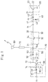
Figure 1 is a circuit diagram of a transmitter-receiver
circuit for a wireless communication unit according to the
first embodiment of the present invention.
Figure 2 is an equivalent circuit diagram where the
transmitter-receiver circuit for a wireless communication
unit according to the first embodiment of the present invention
performs receiving operation.
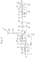
Figure 3 is a circuit diagram of a transmitter-receiver
circuit for a wireless communication unit according to the
second embodiment of the present invention.
Figure 4 is an equivalent circuit diagram where the
transmitter-receiver circuit for a wireless communication
unit according to the second embodiment of the present invention
performs receiving operation.
Figures 5(a) through 5(d) are circuit diagrams illustrating
variations of a second matching circuit and an output
terminal of a received signal in the transmitter-receiver
circuit for a wireless communication unit according to the
second embodiment of the present invention.
Figures 6(a) through 6(d) are circuit diagrams illustrating
variations of the second matching circuit and the
output terminal of the received signal in the transmitter-receiver
circuit for a wireless communication unit according
to the second embodiment of the present invention.
Figure 7 is a circuit diagram of a transmitter-receiver
circuit where GaAs FETs are used for a semiconductor integrated
circuit device according to the third embodiment of
the present invention.
Figure 8 is a circuit diagram of a transmitter-receiver
circuit where GaAs FETs are used for a semiconductor integrated
circuit device according to the fourth embodiment of
the present invention.
Figure 9 is a circuit diagram of a transmitter-receiver
circuit for a wireless communication unit according to the
fifth embodiment of the present invention.
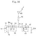
Figure 10 is an equivalent circuit diagram where the
transmitter-receiver circuit for a wireless communication
unit according to the fifth embodiment of the present invention
performs transmitting operation.
Figure 11 is a circuit diagram of a conventional transmitter-receiver
circuit of a digital type using FETs.
BEST MODE FOR CARRYING OUT THE INVENTION
FIRST EMBODIMENT
Hereinafter, the first embodiment of the present invention
will be described with reference to the drawings.
Figure 1 is a circuit diagram of a transmitter-receiver
circuit for a wireless communication unit according to the
first embodiment of the present invention. In Figure 1, 10
denotes a transmitter amplifier for amplifying an input signal
to be transmitted and then outputting the amplified signal. 20
denotes a low-noise receiver amplifier for amplifying an input
received signal and then outputting the amplified signal. 30
denotes a mode switch for switching transmission state and reception
state in a time-division manner. 40 denotes a first
matching circuit for matching the impedance of the input received
signal with the input impedance of the low-noise receiver
amplifier 20. 50 denotes a second matching circuit for
matching the output impedance of the transmitter amplifier 10
with predetermined impedance. 60 denotes a third matching circuit
for matching the impedance of the input signal to be
transmitted with the input impedance of a high-power FET 12 of
the transmitter amplifier 10. 70 denotes an interconnection,
having characteristic impedance of 50Ω, for connecting the
mode switch 30, the transmitter amplifier 10 and an antenna 80
used for both transmission and reception with each other. 71
denotes coupling capacitance for ac coupling the mode switch
30 to the first matching circuit 40.
In the transmitter amplifier 10 shown in Figure 1, 11
denotes an input terminal, through which a signal to be
transmitted is input 12 denotes a high-power FET, of which
the gate electrode is provided with the input signal to be
transmitted via the third matching circuit 60 and the source
is grounded. 13 denotes a power supply terminal connected to
the drain electrode of the high-power FET 112. 14 denotes a
control terminal connected to the gate electrode of the high-power
FET 12 via resistance. 15A denotes an output terminal
connected to the antenna 80 through an interconnection 70
having characteristic impedance of 50Ω and to an input terminal
31 of the mode switch 30.
In the low-noise receiver amplifier 20 shown in Figure
11, 21 denotes an input terminal, through which a received
signal is input via the first matching circuit 40. 22 denotes
a low-noise FET, of which the gate electrode is provided
with the received signal and the source is grounded. 23
denotes an output terminal connected to the drain electrode
of the low-noise FET 22.
In the mode switch 30 shown in Figure 1, 31 denotes an
input terminal connected to the antenna 80 through the inter-connection
70 having characteristic impedance of 50Ω and to
the output terminal 15A of the transmitter amplifier 10. 32
denotes a switch-control-signal input terminal for controlling
a switching FET 34. 33 denotes an output terminal, through
which the received signal, input through the antenna 80, is
output.
In the first matching circuit 40 shown in Figure 1, 41
denotes an input terminal connected to the output terminal 33
of the mode switch 30 via the coupling capacitance 71. 42
denotes an output terminal connected to the input terminal 21
of the low-noise receiver amplifier 20. 43 denotes a first
inductor, one end of which is connected to the input terminal
41 and the other end of which is grounded, for constituting
the first matching circuit 40. 44 denotes a second inductor,
one end of which is connected to the input terminal 41 and
the other end of which is connected to the output terminal
42, for constituting the first matching circuit 40.
In the second matching circuit 50 shown in Figure 1, 51
denotes a first capacitor, one end of which is connected to
the drain electrode of the high-power FET 12 and the other
end of which is grounded, for constituting the second matching
circuit 50. 52 denotes an inductor, one end of which is
connected to the drain electrode of the high-power FET 12 and
the other end of which is connected to a second capacitor 53,
for constituting the second matching circuit 50. 53 denotes
a second capacitor, one end of which is connected to the inductor
52 and the other end of which is connected to the output
terminal 15A, for constituting the second matching
circuit 50.
In the third matching circuit 60 shown in Figure 1, 61
denotes a first capacitor, one end of which is connected to
the input terminal 11 of the transmitter amplifier 10 and the
other end of which is connected to an inductor 62, for constituting
the third matching circuit. 62 denotes the inductor,
one end of which is connected to the first capacitor 61
and the other end of which is connected to the gate electrode
of the high-power FET 12 of the transmitter amplifier 10, for
constituting the third matching circuit 60. 63 denotes a
second capacitor, one end of which is connected to the inductor
62 and the gate electrode of the high-power FET 12 and
the other end of which is grounded, for constituting the
third matching circuit.
In this embodiment, the FETs constituting the transmitter
amplifier 10, the low-noise receiver amplifier 20 and the
mode switch 30 are assumed to be GaAs FETs or silicon MOS-FETs.
Hereinafter, the operation of the transmitter-receiver
circuit having the above-described configuration will be described
with reference to Figures 1 and 2.
Figure 2 is an equivalent circuit diagram where the
transmitter-receiver circuit for a wireless communication
unit according to the first embodiment of the present invention
performs receiving operation. In Figure 2, the same
components as those of the transmitter-receiver circuit shown
in Figure 1 are identified by the same reference numerals and
the description thereof will be omitted herein.
First, the operation thereof during reception will be
described.
As shown in Figure 1, a less intense received signal,
which has been input through the antenna 80, passes through
the interconnection 70 having characteristic impedance of 50 Ω
and is input to the mode switch 30.
In the mode switch 30, the switching FET 34 has been
turned ON responsive to the control signal input through the
switch-control-signal input terminal 32. Thus, the input received
signal is next passed through the switching FET 34,
the output terminal 33 of the mode switch 30 and the coupling
capacitance 71 so as to be input to the first matching circuit
40.
Subsequently, the impedance of the input received signal
is matched with the input impedance of the low-noise receiver
amplifier 20. Thereafter, the signal is input to the input
terminal 21 of the low-noise receiver amplifier 20. At this
point in time, by turning ON the high-power FET 12 upon the
application of a control voltage to the control terminal 14
of the high-power FET 12 in the transmitter amplifier 10, the
high-power FET 12 can be equivalent to pure resistance 12A as
shown in Figure 2. Thus, the circuit section on the transmission
can be short-circuited during reception. Accordingly,
the input impedance of the low-noise receiver amplifier 20
can be matched by the first inductor 43 and the second inductor
44 constituting the first matching circuit 40 and the inductor
52 constituting the second matching circuit 50.
Next, the received signal input to the low-noise receiver
amplifier 20 is amplified by the low-noise FET 22 and then
output through the output terminal 23 of the low-noise receiver
amplifier 20.
It is noted that, if the transmitter amplifier 10 performs
multiple-stage amplification using a plurality of FETs,
the control terminal 14 may be provided for the FET on the
last amplification stage.
Next, the operation thereof during transmission will be
described with reference to Figure 1.
First, a signal to be transmitted, which has been modulated
and amplified to reach a predetermined signal level, is
input to the input terminal 11 of the transmitter amplifier
10.
Then, after the impedance of the input signal to be
transmitted is matched by the third matching circuit 60 with
the input impedance of the high-power FET 12, the input signal
to be transmitted is amplified by the high-power FET 12
to gain predetermined power.
Subsequently, after having been subjected to the impedance
conversion by the second matching circuit 50, the amplified
signal to be transmitted is passed through the
interconnection 70 having characteristic impedance of 50Ω,
input to the antenna 80 and then output by the antenna 80 as
radio waves. Since the switching FET 34 is turned OFF in the
mode switch 30, the circuit section on the reception side is
isolated from the antenna 80 and the transmitter amplifier 10.
This embodiment is characterized in that the transmitter
amplifier 10 can be connected to the antenna 80 without interposing
any switch therebetween by matching the inputs to
the low-noise receiver amplifier 20 using the output impedance
of the transmitter amplifier 10 during the OFF state and
the output impedance of the first matching circuit 40 to the
low-noise receiver amplifier 20. Thus, since the switch for
transmission need not be used, the pass loss caused by a
switching device on the output signal of the transmitter amplifier
10 can be eliminated. As a result, low power consumption
is realized during transmission.
In addition, since only one switching FET is necessary,
the mode switch can have a reduced area and can be integrated
more highly.
The value of resistance where the control terminal 14 of
the high-power FET 12 is used as having been turned ON by applying
a voltage to the control terminal 14 during the transmission
OFF state is equal to or lower than 1Ω, which is the
ON resistance of a generally used FET. Thus, the influence
of the resistance on the input matching of the low-noise receiver
amplifier 20 is negligible.
SECOND EMBODIMENT
Hereinafter, the second embodiment of the present invention
will be described with reference to the drawings.
Figure 3 is a circuit diagram of a transmitter-receiver
circuit for a wireless communication unit according to the
second embodiment of the present invention. In Figure 3, 10
denotes a transmitter amplifier for amplifying an input signal
to be transmitted and then outputting the amplified signal. 20
denotes a low-noise receiver amplifier for amplifying an input
received signal and then outputting the amplified signal. 30
denotes a mode switch for switching transmission state and reception
state in a time-division manner. 40 denotes a first
matching circuit for matching the impedance of the input received
signal with the input impedance of the low-noise receiver
amplifier 20. 50 denotes a second matching circuit for
matching the output impedance of the transmitter amplifier 10
with predetermined impedance. 60 denotes a third matching circuit
for matching the impedance of the input signal to be
transmitted with the input impedance of a high-power FET 12 of
the transmitter amplifier 10. 70 denotes an interconnection,
having characteristic impedance of 50Ω, for connecting a terminal
15B functioning as output terminal for transmission and
input terminal for reception of the transmitter amplifier 10
to the antenna 80 used for both transmission and reception.
71 denotes coupling capacitance for ac coupling the mode
switch 30 to the first matching circuit 40. In Figure 3, the
same components as those of the circuits shown in Figure 1
are identified by the same reference numerals and the description
thereof will be omitted herein.
This embodiment is different from the first embodiment in
that the input terminal 31 of the mode switch 30 is connected
not to the terminal 15B functioning as output terminal for
transmission and input terminal for reception of the transmitter
amplifier 10, but to an output terminal 16 of the received
signal. The output terminal 16 is used in common both as a
terminal of the drain electrode of the high-power FET 12 and
as a non-grounded terminal of the first capacitor 51 in the
second matching circuit 50.
Hereinafter, the operation of the transmitter-receiver
circuit having the above-described configuration will be described
with reference to Figures 3 and 4.
The operation thereof during transmission is the same as
that of the transmitter-receiver circuit described in the
first embodiment, and thus the description thereof will be
omitted herein. Only the operation thereof during reception
will be described hereinafter.
Figure 4 is an equivalent circuit diagram where the
transmitter-receiver circuit for a wireless communication
unit according to the second embodiment performs receiving
operation.
First, as shown in Figure 3, a less intense received
signal, which has been input through the antenna 80, passes
through the interconnection 70 having characteristic impedance
of 50Ω, the terminal 15B functioning as output terminal
for transmission and input terminal for reception of the
transmitter amplifier 10 and the second matching circuit 50,
and then is input to the mode switch 30.
In the mode switch 30, the switching FET 34 has been
turned ON responsive to the control signal input through the
switch-control-signal input terminal 32. Thus, the input received
signal is next passed through the switching FET 34,
the output terminal 33 of the mode switch 30 and the coupling
capacitance 71 so as to be input to the first matching circuit
40.
Subsequently, the impedance of the input received signal
is matched with the input impedance of the low-noise receiver
amplifier 20 by the first matching circuit 40. Thereafter,
the signal is input to the input terminal 21 of the low-noise
receiver amplifier 20. At this point in time, by turning ON
the high-power FET 12 upon the application of a control voltage
to the control terminal 14 of the high-power FET 12 in
the transmitter amplifier 10, the high-power FET 12 can be
equivalent to pure resistance 12A as shown in Figure 4. Thus,
the circuit section on the transmission side can be short-circuited
during reception. Accordingly, the input impedance
of the low-noise receiver amplifier 20 can be matched by the
first inductor 43 and the second inductor 44 constituting the
first matching circuit 40 and the inductor 52 constituting
the second matching circuit 50.
Next, the received signal input to the low-noise receiver
amplifier 20 is amplified by the low-noise FET 22 and then
output through the output terminal 23 of the low-noise receiver
amplifier 20.
It is noted that, if the transmitter amplifier 10 performs
multiple-stage amplification using a plurality of FETs,
the control terminal 14 may be provided for the FET on the
last amplification stage.
As can be understood, in this second embodiment, the resulting
number of devices can be reduced, for example, by using
the inductor 43 required for the first matching circuit
40 simultaneously as the inductor 52 in the second matching
circuit 50 as shown in Figure 4. As a result, the size of
the first matching circuit 40 can be reduced.
That is to say, during reception, there is no problem if
only impedance matching is realized between the antenna 80
and the low-noise receiver amplifier 20 by using the devices
of the first matching circuit 40 and the second matching circuit.
Thus, by comparison to the first embodiment, the design
flexibility of the first matching circuit 40 can be
increased.
For example, once the first matching circuit 40 is
fixed, the first matching circuit 40 itself cannot be
changed. However, even in such a case, by providing the output
terminal 16 of the received signal at such a position of
the second matching circuit 50 as to optimize the impedance
matching with the low-noise receiver amplifier 20, the first
matching circuit 40 can also be connected to the output terminal
16 of the received signal. Thus, the number of devices
can be reduced simultaneously.
Herein, variations of the second matching circuit 50 and
variations of the output terminal of the received signal at
respective positions corresponding to the respective variations
where impedance matching with the low-noise receiver
amplifier 20 is optimized are illustrated in Figures 5 and 6.
In the second matching circuit 50 shown in Figure 5(a), the
output terminal 16A of the received signal is connected to
the connection point between the inductor 52 and the second
capacitor 53. In the second matching circuit 50A shown in
Figure 5(b), the inductor is divided into two parts 52A and
52B, and the output terminal 16B of the received signal is
connected to the drain electrode of a high-power FET 12 (not
shown) and to a non-grounded terminal, i.e., a common terminal
of the first capacitor 51. In the second matching circuit
50A shown in Figure 5(c), the output terminal 16C of the received
signal is connected to a common terminal of the inductors
52A and 52B. In the second matching circuit 50B shown in
Figure 5(d), one terminal of the inductor 52 is grounded and
the other end thereof is connected to the drain electrode of
the high-power FET 12 and to the non-grounded terminal, i.e.,
the common terminal of the first capacitor 51, to which terminal
the output terminal 16D of the received signal is connected.
In the second matching circuit 50C shown in Figure
6(a), a second inductor 54 is newly added to the second
matching circuit 50, one terminal of the second inductor 54
is grounded and the other end thereof is connected to the
drain electrode of the high-power FET 12 and to the non-grounded
terminal, i.e., the common terminal of the first capacitor
51, to which terminal the output terminal 16E of the
received signal is connected. In the second matching circuit
50C shown in Figure 6(b), the output terminal 16F of the received
signal is connected to the connection point between
the inductor 52 and the second capacitor 53. In the second
matching circuit 50D shown in Figure 6(c), a third capacitor
55 is newly added to the second matching circuit 50C, one
terminal of the third capacitor 55 is grounded and the other
end thereof is connected to the connection point between the
inductor 52 and the second capacitor 53, and the output terminal
16G of the received signal is connected to the drain
electrode of a high-power FET 12 (not shown) and to a non-grounded
terminal, i.e., a common terminal of the first capacitor
51. In the second matching circuit 50D shown in Figure
6(d), the output terminal 16H of the received signal is
connected to a common connection point among the inductor 52,
the second capacitor 53 and the third capacitor 55.
THIRD EMBODIMENT
Hereinafter, the third embodiment of the present invention
will be described with reference to the drawings.
Figure 7 is a circuit diagram of a transmitter-receiver
circuit where GaAs FETs are used for a semiconductor integrated
circuit device according to the third embodiment of
the present invention. That is to say, Figure 7 is a circuit
diagram of a device formed by integrating the transmitter-receiver
circuit for a wireless communication unit as described
in the first embodiment onto a semiconductor substrate.
In Figure 7, 10 denotes a transmitter amplifier for amplifying
an input signal to be transmitted and then outputting
the amplified signal. 20 denotes a low-noise receiver amplifier
for amplifying an input received signal and then outputting
the amplified signal. 30 denotes a mode switch for
switching transmission state and reception state in a time-division
manner. 40 denotes a first matching circuit for
matching the impedance of the input received signal with the
input impedance of the low-noise receiver amplifier 20. 50 denotes
a second matching circuit for matching the output impedance
of the transmitter amplifier 10 with predetermined
impedance. 60 denotes a third matching circuit for matching
the impedance of the input signal to be transmitted with the
input impedance of a high-power FET 12 of the transmitter amplifier
10. 70 denotes an interconnection, having characteristic
impedance of 50Ω, for connecting an input/output terminal
72 on the antenna side to the antenna 80 used for both transmission
and reception. 71 denotes coupling capacitance for ac
coupling the mode switch 30 to the first matching circuit 40.
The respective circuits described above, i.e., the
transmitter amplifier 10 including the second matching circuit
50 and the third matching circuit 60, the low-noise receiver
amplifier 20, the mode switch 30 and the first
matching circuit 40, are formed on a semiconductor substrate
1.
In the transmitter amplifier 10 shown in Figure 7, 11
denotes an input terminal, through which a signal to be
transmitted is input. 12 denotes a high-power FET, of which
the gate electrode is provided with the input signal to be
transmitted via the third matching circuit 60 and the source
is grounded. 13 denotes a power supply terminal connected to
the drain electrode of the high-power FET 12. 14 denotes a
control terminal connected to the gate electrode of the high-power
FET 12. 15A denotes a terminal functioning as output
terminal on the transmission side and input terminal on the
reception side, which is connected to the input/output terminal
72 on the antenna side and to the input terminal 31 of the
mode switch 30.
In the low-noise receiver amplifier 20 shown in Figure
7, 21 denotes an input terminal of the low-noise receiver amplifier
20, through which a received signal is input via the
first matching circuit 40. 22 denotes a low-noise FET, of
which the gate electrode is provided with the received signal
and the source is grounded. 23 denotes an output terminal of
the low-noise receiver amplifier 20 connected to the drain
electrode of the low-noise FET 22.
In the mode switch 30 shown in Figure 7, 31 denotes an
input terminal connected to the antenna 80 through the inter-connection
70 having characteristic impedance of 50Ω and to
the output terminal 15 of the transmitter amplifier 10. 32
denotes a switch-control-signal input terminal for controlling
a switching FET. 33 denotes an output terminal, through which
the received signal, input through the antenna 80, is output.
34 denotes a switching FET constituting the mode switch 30.
In Figure 7, the same components as those of the respective
matching circuits shown in Figure 1 are identified by the same
reference numerals and the description thereof will be omitted
herein.
Since the operation of the semiconductor integrated circuit
device according to this embodiment is the same as that
of the first embodiment, the description thereof will be omitted
herein.
In accordance with this embodiment, the transmitter amplifier
10 can be connected to the antenna 80 without interposing
any switch therebetween by matching the inputs to the
low-noise receiver amplifier 20 while using, in combination,
the output impedance of the transmitter amplifier 10 during
the OFF state and the output impedance of the first matching
circuit 40 to the low-noise receiver amplifier 20. Thus,
since the use of a switch for transmission is no longer necessary,
it is possible to eliminate the pass loss that is ordinarily
caused by a switching device on the output signal of
the transmitter amplifier 10. As a result, the power consumption
can be reduced during transmission.
In addition, since only one switching FET is required,
the area occupied by the mode switch on the transmitter-receiver
circuit can be narrowed, high integration is enabled.
Ultimately, this fact can contribute to downsizing and cost
reduction of a wireless communication unit incorporating the
semiconductor integrated circuit device according to this embodiment.
In this embodiment, GaAs FETs are used as the FETs constituting
the transmitter amplifier 10, the low-noise receiver
amplifier 20 and the mode switch 30. Alternatively, these FETs
may be silicon MOSFETs.
The value of resistance where the control terminal 14 of
the high-power FET 12 is used as having been turned ON by applying
a voltage to the control terminal 14 during the transmission
OFF state is equal to or lower than 1Ω, which is the
ON resistance of a generally used FET. Thus, the influence
of the resistance on the input matching of the low-noise receiver
amplifier 20 is negligible.
FOURTH EMBODIMENT
Hereinafter, the fourth embodiment of the present invention
will be described with reference to the drawings.
Figure 8 is a circuit diagram of a transmitter-receiver
circuit where GaAs FETs are used for a semiconductor integrated
circuit device according to the fourth embodiment of
the present invention. That is to say, Figure 8 is a circuit
diagram of a device formed by integrating the transmitter-receiver
circuit for a wireless communication unit as described
in the second embodiment onto a semiconductor substrate.
In Figure 8, 10 denotes a transmitter amplifier for amplifying
an input signal to be transmitted and then outputting
the amplified signal. 20 denotes a low-noise receiver amplifier
for amplifying an input received signal and then outputting
the amplified signal. 30 denotes a mode switch for
switching transmission state and reception state in a time-division
manner. 40 denotes a first matching circuit for
matching the impedance of the input received signal with the
input impedance of the low-noise receiver amplifier 20. 50 denotes
a second matching circuit for matching the output impedance
of the transmitter amplifier 10 with predetermined
impedance. 60 denotes a third matching circuit for matching
the impedance of the input signal to be transmitted with the
input impedance of a high-power FET 12 of the transmitter amplifier
10. 70 denotes an interconnection, having characteristic
impedance of 50Ω, for connecting an input/output terminal
72 on the antenna side to the antenna 80 used for both transmission
and reception. 71 denotes coupling capacitance for ac
coupling the mode switch 30 to the first matching circuit 40.
It is noted that the same components as those of the respective
circuits shown in Figure 3 are identified by the same
reference numerals and the description thereof will be omitted
herein.
The respective circuits described above, i.e., the
transmitter amplifier 10 including the second matching circuit
50 and the third matching circuit 60, the low-noise receiver
amplifier 20, the mode switch 30 and the first
matching circuit 40, are formed on a semiconductor substrate
1.
The fourth embodiment is characterized in that the input
terminal 31 of the mode switch 30 is not connected to the
terminal 15B functioning as output terminal for transmission
and input terminal for reception of the transmitter amplifier
10, but to the output terminal 16 of the received signal in
the second matching circuit 50.
The operations thereof during reception and transmission
are the same as those of the transmitter-receiver circuit as
described in the second embodiment. Thus, the description
thereof will be omitted herein.
In accordance with the fourth embodiment, by turning ON
the high-power FET 12 upon the application of a control voltage
to the control terminal 14 of the high-power FET 12 in
the transmitter amplifier 10 shown in Figure 8 and by using
the high-power FET 12 as pure resistance 12A, the circuit
section on the transmission side can be short-circuited and
isolated during reception.
Thus, the resulting number of devices can be reduced by
using the inductor required for the first matching circuit 40
simultaneously as the inductor 52 in the second matching circuit
50 as shown in Figure 8. As a result, the size of the
first matching circuit 40 can be reduced.
That is to say, during reception, there is no problem if
only impedance matching is realized between the antenna 80
and the low-noise receiver amplifier 20 by using the devices
of the first matching circuit 40 and the second matching circuit.
Thus, by comparison to the third embodiment, the design
flexibility of the first matching circuit 40 can be increased.
For example, by providing the output terminal 16 of
the received signal at such a position of the second matching
circuit 50 as to optimize the impedance matching with the
low-noise receiver amplifier 20, the input terminal 31 of the
mode switch 30 can also be connected to the output terminal
16 of the received signal. Thus, the number of devices can
be reduced simultaneously. In this case, it is naturally
possible to apply the respective variations 50A through 50D
of the second matching circuit 50 shown in Figures 5 and 6
and the respective variations of the output terminals 16A to
16H of the received signal corresponding to the respective
variations.
In addition, since only one switching FET is required,
the area occupied by the mode switch 30 and the first matching
circuit 40 on the transmitter-receiver circuit can be narrowed,
high integration is realized more easily. Ultimately,
this fact can contribute more to downsizing and cost reduction
of a wireless communication unit incorporating the semiconductor
integrated circuit device according to this embodiment.
FIFTH EMBODIMENT
Hereinafter, the fifth embodiment of the present invention
will be described with reference to the drawings.
Figure 9 is a circuit diagram of a transmitter-receiver
circuit for a wireless communication unit according to the
fifth embodiment of the present invention.
The fifth embodiment is characterized by the configuration
in which the transmission/reception mode switch is not
connected between the antenna and the low-noise receiver amplifier
as is done in the foregoing embodiments, but is connected
between the antenna and the transmitter amplifier. In
Figure 9, 10 denotes a transmitter amplifier for amplifying an
input signal to be transmitted and then outputting the amplified
signal. 20 denotes a low-noise receiver amplifier for amplifying
an input received signal and then outputting the
amplified signal. 30 denotes a mode switch for switching
transmission state and reception state in a time-division manner.
40 denotes a first matching circuit for matching the impedance
of the input received signal with the input impedance
of the low-noise receiver amplifier 20. 50 denotes a second
matching circuit for matching the output impedance of the
transmitter amplifier 10 with predetermined impedance. 60 denotes
a third matching circuit for matching the impedance of
the input signal to be transmitted with the input impedance of
a high-power FET 12 of the transmitter amplifier 10. 70 denotes
an interconnection, having characteristic impedance of
50Ω, for connecting the mode switch 30, the first matching
circuit 40 and an antenna 80 used for both transmission and
reception to each other. 71 denotes coupling capacitance for
ac coupling the mode switch 30 to the first matching circuit
40.
In the transmitter amplifier 10 shown in Figure 9, 11
denotes an input terminal, through which a signal to be
transmitted is input. 12 denotes a high-power FET, of which
the gate electrode is provided with the input signal to be
transmitted via the third matching circuit 60 and the source
is grounded. 13 denotes a power supply terminal connected to
the drain electrode of the high-power FET 112. 15A denotes
an output terminal connected to the input terminal 31 of the
mode switch 30.
In the low-noise receiver amplifier 20 shown in Figure
9, 21 denotes an input terminal, through which a received
signal is input via the coupling capacitance 71 and the first
matching circuit 40. 22 denotes a low-noise FET, of which the
gate electrode is provided with the received signal and the
source is grounded. 23 denotes an output terminal connected
to the drain electrode of the low-noise FET 22. 24 denotes a
control terminal connected to the gate electrode of the low-noise
FET 22.
In the mode switch 30 shown in Figure 9, 31 denotes an
input terminal connected to the output terminal 15 of the
transmitter amplifier 10. 32 denotes a switch-control-signal
input terminal for controlling a switching FET. 33 denotes an
output terminal, through which the amplified signal to be
transmitted is output to the antenna 80. 34 denotes a switching
FET constituting the mode switch 30.
In the first matching circuit 40 shown in Figure 9, 41
denotes an input terminal connected to the antenna 80 and to
the output terminal 33 of the mode switch 30 via the coupling
capacitance 71 and an interconnection having characteristic
impedance of 50Ω. 42 denotes an output terminal connected to
the input terminal 21 of the low-noise receiver amplifier 20.
43 denotes a first inductor, one end of which is connected to
the input terminal 41 of the first matching circuit 40 and
the other end of which is grounded, for constituting the
first matching circuit 40. 44 denotes a second inductor, one
end of which is connected to the input terminal 41 of the
first matching circuit 40 and the other end of which is connected
to the output terminal 42, for constituting the first
matching circuit 40.
In the second matching circuit 50 shown in Figure 1, 51
denotes a first capacitor, one end of which is connected to
the drain electrode of the high-power FET and the other end
of which is grounded, for constituting the second matching
circuit 50. 52 denotes an inductor, one end of which is connected
to the drain electrode of the high-power FET and the
other end of which is connected to a second capacitor 53, for
constituting the second matching circuit 50. 53 denotes a
second capacitor, one end of which is connected to the inductor
52 and the other end of which is connected to the output
terminal 15A of the transmitter amplifier 10, for constituting
the second matching circuit 50.
All of the FETs constituting the transmitter amplifier
10, the low-noise receiver amplifier 20 and the mode switch
30 of this transmitter-receiver circuit are assumed to be
GaAs FETs or silicon MOSFETs.
Hereinafter, the operation of the transmitter-receiver
circuit having the above-described configuration will be described
with reference to Figures 9 and 10.
Figure 10 is an equivalent circuit diagram where the
transmitter-receiver circuit for a wireless communication
unit according to the fifth embodiment of the present invention
performs transmitting operation. In Figure 10, the same
components as those of the transmitter-receiver circuit shown
in Figure 9 are identified by the same reference numerals and
the description thereof will be omitted herein.
First, the operation thereof during reception will be
described.
A less intense received signal, which has been input
through the antenna 80, passes through the interconnection 70
having characteristic impedance of 50Ω and is input to the
first matching circuit 40 shown in Figure 9 via the coupling
capacitance 71.
Subsequently, the impedance of the input received signal
is matched with the input impedance of the low-noise receiver
amplifier 20 by the first matching circuit 40. Thereafter,
the signal is input to the input terminal 21 of the low-noise
receiver amplifier 20. The input received signal is amplified
by the low-noise FET 22 and then output through the output
terminal 23 of the low-noise receiver amplifier 20. Since the
switching FET 34 has been turned OFF in the mode switch 30,
the circuit section on the transmission side is isolated from
the antenna 80 and the low-noise receiver amplifier 20.
Next, the operation thereof during transmission will be
described.
First, a signal to be transmitted, which has been modulated
and amplified to reach a predetermined signal level, is
input to the input terminal 11 of the transmitter amplifier
10.
Then, after the impedance of the input signal to be
transmitted is matched by the third matching circuit 60 with
the input impedance of the high-power FET 12, the input signal
to be transmitted is amplified by the high-power FET 12
to gain desired power.
At this point in time, by turning ON the low-noise FET
22 upon the application of a positive voltage, which is equal
to larger than Schottky voltage, to the control terminal 24
of the low-noise FET 22 in the low-noise receiver amplifier
20 shown in Figure 9, the low-noise FET 22 can be equivalent
to pure resistance 22A as shown in Figure 10. Thus, the circuit
section on the reception side can be short-circuited
during transmission. Accordingly, the output impedance of
the transmitter amplifier 10 can be matched with predetermined
impedance by the first inductor 43 and the second inductor
44 constituting the first matching circuit 40 and the
inductor 52 constituting the second matching circuit 50.
Next, the signal to be transmitted, subjected to the impedance
matching, passes through the interconnection 70 having
characteristic impedance of 50 Ω and is input to the
antenna 80 so as to be output through the antenna 80 as radio
waves.
It is noted that the impedance matching should be performed
between the first matching circuit and the second
matching circuit so that the amplified signal to be transmitted
does not flow toward the low-noise receiver amplifier 20.
As can be understood from the above description, in the
fifth embodiment, the outputs of the transmitter amplifier 10
are matched by using, in combination, the impedance of the
low-noise receiver amplifier 20 during the OFF state and the
impedance of the second matching circuit 50 in the transmitter
amplifier 10 whereby the low-noise receiver amplifier 20
can be connected to the antenna 80 without interposing any
switch. As a result, since a switch for reception can be
omitted, it is possible to eliminate the pass loss, which is
ordinarily caused by a switch on the input signal of the low-noise
receiver amplifier 20.
Furthermore, since the less intense received signal is
not attenuated, the S/N ratio during amplification can be increased.
Moreover, since only one switching FET is enough, a
switch can be downsized and highly integrated.
INDUSTRIAL APPLICABILITY
As is apparent from the foregoing description, in the
transmitter-receiver circuit for a wireless communication
unit according to the present invention, the output terminal
of the transmitter amplifier is directly connected to the antenna
without passing through the mode switch during transmission.
Thus, the pass loss, ordinarily caused by a switch on
a signal to be transmitted, can be eliminated. As a result,
the power consumption can be reduced. On the other hand, during
reception, the circuit section on the transmission side is
short-circuited by using the FET for transmission amplification
as resistance. As a result, a mode switch on the transmission
side is no longer necessary. In other words, a mode
switch on the reception side may be constituted by only one
switching device, and thus the area occupied by the mode
switch in the entire circuit can be reduced. Consequently, the
overall size of the transmitter-receiver circuit can be reduced.
On the other hand, since the semiconductor integrated
circuit device according to the present invention is constituted
by the transmitter-receiver circuit for a wireless communication
unit according to the present invention, the power
consumption during transmission can be reduced and the overall
size of the transmitter-receiver circuit can be reduced.
Thus, the present invention is advantageous for even higher
integration. As a result, the costs of a semiconductor integrated
circuit device can be reduced.