EP0876016A1 - Digitales Verfahren zur adaptiven Taktrückgewinnung - Google Patents
Digitales Verfahren zur adaptiven Taktrückgewinnung Download PDFInfo
- Publication number
- EP0876016A1 EP0876016A1 EP97400992A EP97400992A EP0876016A1 EP 0876016 A1 EP0876016 A1 EP 0876016A1 EP 97400992 A EP97400992 A EP 97400992A EP 97400992 A EP97400992 A EP 97400992A EP 0876016 A1 EP0876016 A1 EP 0876016A1
- Authority
- EP
- European Patent Office
- Prior art keywords
- buffer
- fill level
- clock
- frequency
- cells
- Prior art date
- Legal status (The legal status is an assumption and is not a legal conclusion. Google has not performed a legal analysis and makes no representation as to the accuracy of the status listed.)
- Granted
Links
- 238000011084 recovery Methods 0.000 title claims abstract description 55
- 230000003044 adaptive effect Effects 0.000 title claims abstract description 40
- 239000000872 buffer Substances 0.000 claims abstract description 159
- 238000001914 filtration Methods 0.000 claims abstract description 7
- 230000007246 mechanism Effects 0.000 claims description 42
- 238000000034 method Methods 0.000 claims description 26
- 238000012986 modification Methods 0.000 claims description 7
- 230000004048 modification Effects 0.000 claims description 7
- 230000005540 biological transmission Effects 0.000 claims description 4
- 238000012544 monitoring process Methods 0.000 claims description 4
- 230000004044 response Effects 0.000 claims description 4
- 230000006870 function Effects 0.000 description 12
- 238000005516 engineering process Methods 0.000 description 6
- 238000010586 diagram Methods 0.000 description 4
- 230000001360 synchronised effect Effects 0.000 description 3
- 230000006978 adaptation Effects 0.000 description 2
- 230000001934 delay Effects 0.000 description 2
- 235000003642 hunger Nutrition 0.000 description 2
- 230000037351 starvation Effects 0.000 description 2
- 230000004308 accommodation Effects 0.000 description 1
- 230000004075 alteration Effects 0.000 description 1
- 230000006727 cell loss Effects 0.000 description 1
- 238000012937 correction Methods 0.000 description 1
- 230000001419 dependent effect Effects 0.000 description 1
- 238000013461 design Methods 0.000 description 1
- 238000001514 detection method Methods 0.000 description 1
- 239000000284 extract Substances 0.000 description 1
- 230000010365 information processing Effects 0.000 description 1
- 238000009434 installation Methods 0.000 description 1
- 230000007774 longterm Effects 0.000 description 1
- RPOCQUTXCSLYFJ-UHFFFAOYSA-N n-(4-ethylphenyl)-2-(2-methyl-3,5-dioxothiomorpholin-4-yl)acetamide Chemical compound C1=CC(CC)=CC=C1NC(=O)CN1C(=O)C(C)SCC1=O RPOCQUTXCSLYFJ-UHFFFAOYSA-N 0.000 description 1
- 230000003287 optical effect Effects 0.000 description 1
- 230000009467 reduction Effects 0.000 description 1
- 238000005070 sampling Methods 0.000 description 1
- 230000011218 segmentation Effects 0.000 description 1
- 238000004088 simulation Methods 0.000 description 1
- 230000000087 stabilizing effect Effects 0.000 description 1
- 238000006467 substitution reaction Methods 0.000 description 1
- 238000012546 transfer Methods 0.000 description 1
Images


Classifications
-
- H—ELECTRICITY
- H04—ELECTRIC COMMUNICATION TECHNIQUE
- H04Q—SELECTING
- H04Q11/00—Selecting arrangements for multiplex systems
- H04Q11/04—Selecting arrangements for multiplex systems for time-division multiplexing
- H04Q11/0428—Integrated services digital network, i.e. systems for transmission of different types of digitised signals, e.g. speech, data, telecentral, television signals
- H04Q11/0478—Provisions for broadband connections
-
- H—ELECTRICITY
- H04—ELECTRIC COMMUNICATION TECHNIQUE
- H04J—MULTIPLEX COMMUNICATION
- H04J3/00—Time-division multiplex systems
- H04J3/02—Details
- H04J3/06—Synchronising arrangements
- H04J3/062—Synchronisation of signals having the same nominal but fluctuating bit rates, e.g. using buffers
- H04J3/0632—Synchronisation of packets and cells, e.g. transmission of voice via a packet network, circuit emulation service [CES]
-
- H—ELECTRICITY
- H04—ELECTRIC COMMUNICATION TECHNIQUE
- H04L—TRANSMISSION OF DIGITAL INFORMATION, e.g. TELEGRAPHIC COMMUNICATION
- H04L12/00—Data switching networks
- H04L12/54—Store-and-forward switching systems
- H04L12/56—Packet switching systems
- H04L12/5601—Transfer mode dependent, e.g. ATM
- H04L2012/5672—Multiplexing, e.g. coding, scrambling
- H04L2012/5674—Synchronisation, timing recovery or alignment
-
- H—ELECTRICITY
- H04—ELECTRIC COMMUNICATION TECHNIQUE
- H04L—TRANSMISSION OF DIGITAL INFORMATION, e.g. TELEGRAPHIC COMMUNICATION
- H04L12/00—Data switching networks
- H04L12/54—Store-and-forward switching systems
- H04L12/56—Packet switching systems
- H04L12/5601—Transfer mode dependent, e.g. ATM
- H04L2012/5678—Traffic aspects, e.g. arbitration, load balancing, smoothing, buffer management
- H04L2012/5681—Buffer or queue management
Definitions
- the invention relates to a method and apparatus for digital clock recovery, in particular for a packet oriented network environment.
- a packet oriented transmission technology for the realization of Broadband Integrated Service Networks is the technology called Asynchronous Transfer Mode (ATM).
- ATM Asynchronous Transfer Mode
- CBR constant bit rate
- circuit emulation The accommodation of constant bit rate (CBR) services by ATM is particularly important, for compatibility with existing systems and future networks, even if ATM is more suitable to the transport of bursty traffic, such as data.
- One of the critical issues of circuit emulation is the recovery of clock frequency of the source data (the service clock frequency) at the receiver.
- ATM's basic transport entity is a 53 byte cell. Five of these bytes are header bytes, and convey information such as link-to-link routing, error correction, service information (priority, payload identifier), and cell type identification.
- a protocol stack is defined by ITU-T for ATM technology, in which the so-called ATM layer performs operations typically found in layers 2 and 3 of the OSI model.
- ATM layer Above the ATM layer is an ATM adaptation layer (AAL), which is divided into segmentation and reassembling layers (SAR) and a convergence sublayer (CS). Five different types of AAL have been defined by ITU-T, covering various applications.
- the AAL-1 (ATM Adaptation layer 1) is devoted to CBR services.
- the AAL1 SAR for functions including timing recovery and cell loss detection which leaves 47 data bytes (376 bits).
- the data is segmented into cells of 47 bytes, an SAR byte is then added to each cell, the 48 bytes are mapped in an ATM cell and are then sent through the network.
- cell jitter As a result of statistical multiplexing of cells at the source and of queuing delays incurred in ATM switches, successive cells arrive to the destination aperiodically.
- the deviation from ideal arrival time is called cell jitter or cell delay variation (CDV).
- CDV cell delay variation
- Cell jitter is composed of a relatively high frequency stuffing jitter and of a low frequency waiting time jitter. The problem with cell jitter is that it can be very large, and except for the fact that its average is zero, its characteristics are mostly unknown.
- Jitter is defined as the higher frequency characteristics of a phase variation on a given clock signal.
- Wander is the lower frequency part of this phase variation. Both are commonly measured in terms of unit intervals (UI), where one UI corresponds to one cycle of the clock signal.
- ITU-T recommendation G.823 has precisely defined output jitter limits that must be met if the system is to be compatible with any CBR equipment. The bounds on maximum peak-to-peak output jitter for 2.048 Mbits.s -1 CBR services are shown in Table 1. Frequency 20Hz - 18kHz 18kHz - 100kHz Jitter 1.5 UI 0.2 UI
- a first method is referred to as the "synchronous method” and is based on the availability of a common network reference clock between the source and the receiver end equipment. This network clock is distributed by the network, and is available either through the Synchronous Digital Hierarchy (SDH) network or its North American version Synchronous Optical NETwork (SONET).
- SDH Synchronous Digital Hierarchy
- SONET North American version Synchronous Optical NETwork
- a second method referred to as the "adaptive method” recovers the service clock based on the fill-level of an incoming cell buffer.
- FIG. 1 of the accompanying drawings illustrates a conventional adaptive clock recovery mechanism 10 formed from a cell buffer 12, a filter 14 and a digitally controlled oscillator 16, responsive to an output of the filter 14.
- a new problem as depicted in the Figures 2A and 2B.
- the output frequency fout is too slow.
- the output frequency fout is still too slow, but cell jitter has appeared.
- cell jitter must be filtered to get a reasonable accuracy. If it is desired accurately to recover the service frequency, the underlying trend in filter fill level evolution must be determined, by filtering the cell jitter.
- an adaptive clock recovery mechanism for an ATM receiver for recovering a service clock transmitted via an ATM network, the mechanism comprising: a first buffer having an input for receiving successive ATM cells from the ATM network and an output; a first buffer fill level controller connected to the first buffer for controlling rates of cell output from the first buffer to be within a predetermined range; a second buffer having an input connected to receive cells from the output of the first buffer and an output; and a second buffer fill level controller connected to the second buffer to cause a rate of cell output from the second buffer to be locked substantially to the service clock frequency.
- the adaptive clock recovery mechanism enables the clock of a constant bit rate (CBR) service to be recovered at an ATM receiver where the service is being emulated from an ATM transmitter.
- CBR constant bit rate
- the provision of the first buffer and the first buffer fill level controller enables cell jitter to be filtered prior to recovery of the service clock.
- An embodiment of the invention can provide adaptive, digital recovery of the service clock at a receiver in a manner which filters the cell jitter and recovers the service clock with acceptable clock jitter.
- the first buffer fill level controller comprises a selectable clock source for supplying a selectable one of at least a first and a second clock frequency for outputting cells from the first buffer, the selectable clock source being responsive to a fill level of the first buffer to select a clock frequency.
- first and second clock frequencies dependent on the fill level of the first buffer provides a simple control structure for keeping the rate of output of cells from the first buffer within a predetermined range.
- the first buffer with its fill level control thus acts as a low pass filter to reduce high frequency cell jitter.
- the first clock frequency has a frequency of fnom+j ppm and the second clock frequency has a frequency of fnom-j ppm, where fnom is a nominal service clock and 2j defines the predetermined range.
- the selectable clock source selects the first clock frequency when a fill level of the first buffer is greater than a threshold value and selects the second clock when a fill level of the first buffer is less than the threshold value.
- the selectable clock source could be a multiple frequency clock signal generator.
- the selectable clock source can comprise a selector having at least first and second clock inputs for respective clock frequencies, a clock output for outputting a clock frequency for controlling the reading of cells from the first buffer and a first buffer fill level input, the selector being arranged to determine a fill level of the coarse buffer and to connect a selected one of the clock inputs to the clock output for supplying a selected clock frequency for controlling the cell output from the first buffer.
- the second buffer fill level controller comprises a phase locked loop, the phase locked loop comprising a filter connected to the second buffer to determine a fill level of the second buffer and a controlled oscillator for providing a clock signal for reading cells from the second buffer, said controlled oscillator having a control input and a clock output, the frequency of the controlled oscillator being controlled by an output of the filter.
- the phase locked loop can provide a stable output frequency locked substantially to the service clock frequency fs.
- the filter comprises a fill level counter for determining a current fill level of the second buffer, a memory for a prior fill level value and a comparator for comparing the current and prior fill levels, the comparator outputting a control signal for modifying an output frequency of the controlled oscillator when the current fill level is higher than the prior fill level by more than a first amount or is less than the prior fill level by more than a second amount.
- the first and second amounts can be the same or different, and can be expressed in absolute or percentage terms are required.
- the prior fill level is preferably a fill level from a previous modification instant, that is the fill level at an instant at which the output frequency of the phase locked loop was last changed.
- the controlled oscillator is a digitally controlled oscillator.
- one or more intermediate fill level controlled buffers may be provided in line between the coarse fill level controlled buffer and the fine fill level controlled buffer to provide different degrees of filtering.
- the invention also provides an ATM receiver circuit and an integrated circuit comprising a mechanism as set out above.
- the invention further provides an ATM receiver comprising a mechanism according as set out above.
- an adaptive clock recovery method for an ATM receiver for recovering a service clock transmitted via the ATM network comprising:
- step (c) comprises:
- step (b) comprises passing the output of the first buffer directly to the input of the second buffer.
- step (b) can comprise one or more intermediate filter steps between steps (a) and (b).
- a method of circuit emulation for CBR services over an ATM network comprising, at an ATM transmitter, transmitting a stream of ATM cells for a CBR source application having a predetermined service clock, and, at an ATM receiver:
- FIG. 3 illustrates an example of an adaptive clock recovery mechanism 20 in accordance with the present invention.
- An incoming stream of ATM cells headers 25 can be received from an SAR header extractor 24 connected to receive ATM cells from a telecommunications line 23.
- the mechanism 20 comprises two buffer levels, or stages 21 and 22.
- the first buffer stage 22 comprises a coarse buffer 26 which receives the incoming cell 25 and acts as a low-pass filter to reduce cell jitter.
- a selector 28 is connected to monitor the fill level of the coarse buffer 26 (for example by comparing the value of in and out pointers for the coarse buffer 26).
- the buffer 26 is configured as a FIFO memory in storage having separate in and out pointers for the next write location and the next read location, respectively.
- the fill level can thus be determined by comparing in and out pointers of the values.
- the selector selects either a first frequency fnom +j from a first oscillator 30 or a second frequency fnom-j from a second oscillator 32 to be supplied to the coarse buffer 26 for controlling the output of cells from the course buffer 26.
- the oscillators could be replaced by a single oscillator and appropriate frequency modification logic.
- the selector 28 and oscillators 30 and 32 could be embodied as a controllable oscillator for outputting either the first or the second frequency in response to the input provided thereto.
- the level of the coarse buffer 26 is over a given value m, it is emptied at a frequency of fnom+j ppm. On the other hand, if the level of the coarse buffer 26 goes below this value, the coarse buffer 26 is emptied at fnom-j ppm.
- fnom is the nominal source frequency (i.e 2,048 Mbit/s for E1 connection and 1,536 Mbit/s for DS1).
- the value of j is chosen so that the maximum empty frequency stays equal or over the tolerated maximum service clock frequency and the minimum empty frequency stays equal or below the minimum service clock frequency. Accordingly, the buffer level is kept between defined bounds (given by the cell delay variation (CDV)), in normal operating mode. In the long term the average of the output frequency of the coarse buffer converges to the source frequency fs.
- CDV cell delay variation
- the output stream of the coarse buffer 26 of the first buffer stage 21 is then fed to a second, Fine, buffer 34, in the second buffer stage 22.
- the buffer 34 is configured as a FIFO memory in storage having separate in and out pointers for the next write location and the next read location, respectively.
- the fill level can thus be determined by comparing in and out pointers of the values.
- the fill level of the fine buffer 34 is used to drive a phase locked loop (PLL) 40 including a filter 36 and a digitally controlled oscillator 38.
- PLL phase locked loop
- the value m which provides the threshold of the selector 28 should be at least equal to N and the size of coarse buffer should at least equal to two times N to avoid cell starvation and overflow which could lead to a dramatic clock recovery situation.
- the fill-level of the fine buffer 34 is sampled every E byte arrivals. If the level difference between the current sample and the previous sample exceeds a threshold thd, the output frequency of the PLL is modified by or below a fixed increment i, as explained with reference to Figure 4.
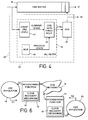
- FIG. 4 illustrates in more detail the structure of the PLL 40, and in particular the PLL filter 36.
- the PLL filter 36 comprises a comparator (CMP) 44, which compares a current fill level determined by a fill level counter 42 to a value stored in a memory 46.
- the value stored in the memory 46 represents the fill level at a previous modification instant.
- the comparison between buffer levels is not done between two consecutive sampling instants, but between the current instant, and a previous modification instant (i.e., when the PLL output frequency was last modified), making sure that a decision is taken each time the buffer level varies of a quantity greater than thd or less than -thd.
- an urgency procedure is set in order to speed up the PLL 40 output frequency if the fine buffer fill level goes beyond or below a given limit to avoid cases of starvation or overflow. It is to be expected that the fine buffer level will raise or lower in significant proportions before stabilizing when lock is achieved.
- the comparator 44 outputting a control signal for modifying an output frequency of the DCO 38 when the current fill level is higher than the prior fill level by more than a first amount (thd) or is less than the prior fill level by more than a second amount (-thd).
- the first and second amounts can be the same or different, and could be expressed in percentage rather than absolute terms.
- the values E and i allows the PLL 40 to lock in a reasonable time.
- the stability of the output frequency once lock is achieved is determined by the threshold thd.
- the PLL 40 output frequency toggles between fnom +ai and fnom +(a+ 1)i, where a is an integer given by: ai ⁇ E ⁇ (a+1)i
- the threshold thd should also be large enough that the fine buffer level lowering, that goes with long periods without cell arrival, is filtered.
- thd is not higher than 2 or 3 bits for most of the time.
- the adaptive clock recovery mechanism described herein could be implemented at least in part by software operating on conventional computing hardware, although in preferred embodiments it is implemented by means of special purpose circuit technology.
- the adaptive clock recovery mechanism can be implemented in any appropriate circuit technology, typically as an integrated circuit, for example using ASIC technology in a manner which will be appropriate to one skilled in the art.
- FIG. 5 is a schematic block representation of an integrated circuit 50 comprising the adaptive clock recovery mechanism 20 of Figure 3.
- certain functional blocks are represented which are related to the clock recovery mechanism 20.
- the integrated circuit 50 can comprise further functional elements according to the specific application of the integrated circuit.
- a cell receiver circuit 52 receives cells from an ATM network. The output of the cell receiver circuit 52 is passed to an SAR header extractor 24, which extracts the header information. The cell data is buffered in a cell FIFO 56. The cell header data is passed to the adaptive clock recovery mechanism 20 of Figure 3. Further control circuitry 58, not shown, can be associated with the adaptive clock mechanism 20.
- the recovered service clock 39 output from the adaptive clock recovery mechanism is associated with the cell data buffered in the cell FIFO 56 and can be passed to circuitry downstream thereof.
- the downstream circuitry can be formed of or comprise line out circuit 56 for local data output as well as other circuitry (not shown).
- Control signal lines are represented by dashed lines in Figure 5.
- Figure 5 also shows a line input 62 for local data input, an SAR header generator 64 and a cell transmission circuit 66 (all of which can be of a conventional design) for transmitting cells to the ATM network.
- the integrated circuit, or discrete circuits could be implemented on, for example, a multimedia interface card for providing voice, etc.
- FIG. 6 is schematic overview of an ATM circuit emulation system in which an embodiment of the present invention may be incorporated.
- first and second interworking function units 72 and 74 communicate with each other via an ATM network 76.
- Each of the interworking function units 72 includes a clock recovery mechanism as described earlier.
- the clock recovery mechanism 20 can be implemented as any suitable device (e.g., an integrated circuit with clock recovery logic for implementing the functions described above on a computer adapter card).
- the first interworking function unit 72 provides an interface between a CBR application 78 having a first service frequency fs1 and the ATM network.
- the second interworking function unit 74 provides an interface between a second CBR application 80 having a second service frequency fs2 and the ATM network.
- the clock recovery mechanism 20 in the second interworking function unit 74 enables the first service clock fs1 to be recovered at the second interworking function unit 74.
- the clock recovery mechanism 20 in the first interworking function unit 72 enables the second service clock fs2 to be recovered at the first interworking function unit 74. In this way circuit emulation can be performed via the ATM network.
- the interworking function units supporting the CBR applications can be any appropriate information processing devices as required for a particular installation, including, by way of example only, computers such as workstations, computer servers, mainframe computers, or video equipment, voice equipment, I/O interface cards for such devices, and so on.
- the fill level of a first buffer receiving a stream of cells is used to provide coarse control of the rate of output of a stream of cells from the first buffer.
- the fill level of a further, fine, buffer receiving said stream of cells from the first buffer is monitored for determining a clock frequency, corresponding to the service clock frequency, for outputting cells from the fine buffer.
- the first buffer fill level control provides low pass cell jitter filtering by selectively supplying a first or a second clock frequency for outputting cells from the first buffer.
- the fine filter fill level control employs a phase locked loop responsive to the current fill level to set a clock frequency for reading out said fine buffer at the service clock frequency. Simulations have demonstrated that embodiments of the invention can recover source frequency at the receiver, under hard conditions, with jitter and wander on the regenerated clocks in the bounds defined by ITU-T. Embodiments of the invention are simple to implement and do not rely on any external clock. Acquisition time of the reception PLL 40 can be significant, but still acceptable.
Landscapes
- Engineering & Computer Science (AREA)
- Computer Networks & Wireless Communication (AREA)
- Multimedia (AREA)
- Computer Hardware Design (AREA)
- Signal Processing (AREA)
- Data Exchanges In Wide-Area Networks (AREA)
- Synchronisation In Digital Transmission Systems (AREA)
Priority Applications (3)
| Application Number | Priority Date | Filing Date | Title |
|---|---|---|---|
| EP97400992A EP0876016B1 (de) | 1997-05-02 | 1997-05-02 | Digitales Verfahren zur adaptiven Taktrückgewinnung |
| DE69735527T DE69735527D1 (de) | 1997-05-02 | 1997-05-02 | Digitales Verfahren zur adaptiven Taktrückgewinnung |
| US09/071,269 US6252850B1 (en) | 1997-05-02 | 1998-05-01 | Adaptive digital clock recovery |
Applications Claiming Priority (1)
| Application Number | Priority Date | Filing Date | Title |
|---|---|---|---|
| EP97400992A EP0876016B1 (de) | 1997-05-02 | 1997-05-02 | Digitales Verfahren zur adaptiven Taktrückgewinnung |
Publications (2)
| Publication Number | Publication Date |
|---|---|
| EP0876016A1 true EP0876016A1 (de) | 1998-11-04 |
| EP0876016B1 EP0876016B1 (de) | 2006-03-22 |
Family
ID=8229750
Family Applications (1)
| Application Number | Title | Priority Date | Filing Date |
|---|---|---|---|
| EP97400992A Expired - Lifetime EP0876016B1 (de) | 1997-05-02 | 1997-05-02 | Digitales Verfahren zur adaptiven Taktrückgewinnung |
Country Status (3)
| Country | Link |
|---|---|
| US (1) | US6252850B1 (de) |
| EP (1) | EP0876016B1 (de) |
| DE (1) | DE69735527D1 (de) |
Cited By (11)
| Publication number | Priority date | Publication date | Assignee | Title |
|---|---|---|---|---|
| WO2000024144A1 (en) * | 1998-10-21 | 2000-04-27 | Tiernan Communications, Inc. | Method and apparatus for de-jittering asynchronous data transfer delay |
| WO2001037468A2 (en) * | 1999-11-19 | 2001-05-25 | Adc Telecommunications, Inc. | Adaptive clock recovery for circuit emulation service |
| US7106758B2 (en) | 2001-08-03 | 2006-09-12 | Adc Telecommunications, Inc. | Circuit and method for service clock recovery |
| US7246192B1 (en) | 2003-01-10 | 2007-07-17 | Marvell International Ltd. | Serial/parallel ATA controller and converter |
| US7263153B2 (en) * | 2002-10-09 | 2007-08-28 | Marvell International, Ltd. | Clock offset compensator |
| US7295644B1 (en) | 2003-07-14 | 2007-11-13 | Marvell International Ltd. | Apparatus for clock data recovery |
| US7864912B1 (en) | 2007-10-19 | 2011-01-04 | Marvell International Ltd. | Circuits, architectures, a system and methods for improved clock data recovery |
| US8260285B2 (en) | 2005-06-14 | 2012-09-04 | St-Ericsson Sa | Performing diagnostics in a wireless system |
| CN103795521A (zh) * | 2014-01-27 | 2014-05-14 | 科大智能(合肥)科技有限公司 | 一种基于以太网传送e1信号的时钟恢复方法及装置 |
| US8930583B1 (en) | 2003-09-18 | 2015-01-06 | Marvell Israel (M.I.S.L) Ltd. | Method and apparatus for controlling data transfer in a serial-ATA system |
| US9432276B1 (en) | 2002-02-13 | 2016-08-30 | Marvell International Ltd. | Systems and methods for compensating a channel estimate for phase and sampling phase jitter |
Families Citing this family (28)
| Publication number | Priority date | Publication date | Assignee | Title |
|---|---|---|---|---|
| SE506080C2 (sv) * | 1996-02-02 | 1997-11-10 | Ericsson Telefon Ab L M | Virtuell tidsslinga |
| WO1999008409A1 (en) * | 1997-08-06 | 1999-02-18 | Telefonaktiebolaget Lm Ericsson | A method and an apparatus for the clock recovery in the transport of constant bit rate services over asynchronous transfer mode |
| US6400683B1 (en) * | 1998-04-30 | 2002-06-04 | Cisco Technology, Inc. | Adaptive clock recovery in asynchronous transfer mode networks |
| ITMI981508A1 (it) * | 1998-07-01 | 2000-01-01 | Alcatel Alstrom Compagnie Gene | Metodo e dispositivo per il controllo numerico del buffer e di un anello ad aggancio di fase per reti asincrone |
| GB9821791D0 (en) * | 1998-10-06 | 1998-12-02 | Sgs Thomson Microelectronics | Data transfer |
| US6731627B1 (en) | 1998-11-17 | 2004-05-04 | Cisco Technology, Inc. | Virtual loop carrier system |
| US6574246B1 (en) * | 1999-02-17 | 2003-06-03 | Tektronix, Inc. | Measuring delay variation of regenerated data clock and of associated data packets |
| US6522671B1 (en) * | 1999-05-10 | 2003-02-18 | Nortel Networks Limited | Protocol independent sub-rate device |
| IT1308746B1 (it) * | 1999-06-22 | 2002-01-10 | Cselt Centro Studi Lab Telecom | Dispositivo per la ricostruzione della temporizzazione di un canaledati trasportato su rete a pacchetto e relativo procedimento. |
| GB9921209D0 (en) * | 1999-09-08 | 1999-11-10 | British Telecomm | Signal switching |
| US6931029B1 (en) * | 2000-02-09 | 2005-08-16 | Nortel Networks Limited | System and method for synchronizing with data received over an unreliable asynchronous medium |
| US6993210B1 (en) * | 2001-03-23 | 2006-01-31 | Ess Technology, Inc. | Imaging system having adaptive clocking in response to processing state |
| US20030021287A1 (en) * | 2001-05-04 | 2003-01-30 | Appian Communications, Inc. | Communicating data between TDM and packet based networks |
| US6990109B2 (en) * | 2001-10-31 | 2006-01-24 | Adtran, Inc. | Method and apparatus for providing reliable voice and voice-band data transmission over asynchronous transfer mode (ATM) network |
| US7319705B1 (en) | 2002-10-22 | 2008-01-15 | Marvell International Ltd. | Programmable pre-emphasis circuit for serial ATA |
| FR2848049B1 (fr) * | 2002-12-03 | 2005-02-18 | France Telecom | Procede de traitement de paquets de donnees recus sur des reseaux asynchrones, et dispositif pour la mise en oeuvre du procede |
| GB2399263A (en) | 2003-03-07 | 2004-09-08 | Zarlink Semiconductor Ltd | Clock synchronisation over a packet network |
| JP3825007B2 (ja) * | 2003-03-11 | 2006-09-20 | 沖電気工業株式会社 | ジッタバッファの制御方法 |
| US20040264961A1 (en) * | 2003-06-12 | 2004-12-30 | Nam Hong Soon | Ethernet passive optical network system, and optical network terminal and optical line terminal provided in the same |
| US7958292B2 (en) | 2004-06-23 | 2011-06-07 | Marvell World Trade Ltd. | Disk drive system on chip with integrated buffer memory and support for host memory access |
| US8094562B1 (en) * | 2004-06-24 | 2012-01-10 | Cypress Semiconductor Corporation | Transmission of a continuous datastream through a re-clocked frame-based transport network |
| US7646836B1 (en) * | 2005-03-01 | 2010-01-12 | Network Equipment Technologies, Inc. | Dynamic clock rate matching across an asynchronous network |
| CN1848717B (zh) * | 2005-04-15 | 2011-04-06 | 华为技术有限公司 | 获得异步解映射时钟的方法及电路 |
| JP2007114840A (ja) * | 2005-10-18 | 2007-05-10 | Nec Electronics Corp | データ同期装置及びそのデータ同期方法 |
| WO2008051123A1 (en) * | 2006-10-27 | 2008-05-02 | Telefonaktiebolaget Lm Ericsson (Publ) | Method for clock recovery using updated timestamps |
| US7924885B2 (en) * | 2006-11-20 | 2011-04-12 | Siverge Networks Ltd | Methods and apparatuses for circuit emulation multi-channel clock recovery |
| DE102007053795A1 (de) | 2007-11-12 | 2009-05-14 | Rohde & Schwarz Gmbh & Co. Kg | Verfahren und Vorrichtung zur Vermeidung von Schwankungen eines digital erzeugten Ausgabetakts |
| US11962677B2 (en) | 2022-04-13 | 2024-04-16 | Stmicroelectronics S.R.L. | System and method for clock resynchronization |
Citations (2)
| Publication number | Priority date | Publication date | Assignee | Title |
|---|---|---|---|---|
| EP0450269A2 (de) * | 1990-03-14 | 1991-10-09 | Alcatel N.V. | Phasenverriegelte Schleifenanordnung |
| EP0707398A1 (de) * | 1994-10-14 | 1996-04-17 | Koninklijke KPN N.V. | Einrichtung zur Steuerung des Pufferlesens für einen ATM-Empfänger |
Family Cites Families (12)
| Publication number | Priority date | Publication date | Assignee | Title |
|---|---|---|---|---|
| FR2594277B1 (fr) * | 1986-02-13 | 1993-04-23 | Houdoin Thierry | Dispositif de synchronisation de paquets par double boucle a verrouillage de phase |
| US4759041A (en) * | 1987-02-19 | 1988-07-19 | Unisys Corporation | Local area network control system synchronization with phase-lock loop |
| BE1000415A7 (nl) * | 1987-03-18 | 1988-11-22 | Bell Telephone Mfg | Asynchroon op basis van tijdsverdeling werkend communicatiesysteem. |
| US5313502A (en) * | 1990-05-09 | 1994-05-17 | Ant Nachrichtentechnik Gmbh | Arrangement for imaging a useful signal from the frame of a first digital signal at a first bite rate into the frame of a second digital signal at a second bite rate |
| DE4217911A1 (de) * | 1992-05-30 | 1993-12-02 | Bundesrep Deutschland | Verfahren und Vorrichtung zur empfangsseitigen Taktrückgewinnung für Digitalsignale |
| US5396492A (en) * | 1993-04-28 | 1995-03-07 | At&T Corp. | Method and apparatus for adaptive clock recovery |
| US5526362A (en) * | 1994-03-31 | 1996-06-11 | Telco Systems, Inc. | Control of receiver station timing for time-stamped data |
| DE4417286A1 (de) * | 1994-05-13 | 1995-11-23 | Deutsche Bundespost Telekom | Verfahren und Schaltungsanordnung zum Auslesen von Daten aus Pufferspeichern in ATM-Einrichtungen |
| GB9410943D0 (en) * | 1994-06-01 | 1994-07-20 | Newbridge Networks Corp | Clock recovery unit |
| GB9601348D0 (en) * | 1996-01-24 | 1996-03-27 | Madge Networks Ltd | Clock synchronisation |
| US6195353B1 (en) * | 1997-05-06 | 2001-02-27 | Telefonaktiebolaget Lm Ericsson (Publ) | Short packet circuit emulation |
| US6111878A (en) * | 1997-11-04 | 2000-08-29 | Alcatel | Low jitter timing recovery technique and device for asynchronous transfer mode (ATM) constant bit rate (CBR) payloads |
-
1997
- 1997-05-02 EP EP97400992A patent/EP0876016B1/de not_active Expired - Lifetime
- 1997-05-02 DE DE69735527T patent/DE69735527D1/de not_active Expired - Lifetime
-
1998
- 1998-05-01 US US09/071,269 patent/US6252850B1/en not_active Expired - Lifetime
Patent Citations (2)
| Publication number | Priority date | Publication date | Assignee | Title |
|---|---|---|---|---|
| EP0450269A2 (de) * | 1990-03-14 | 1991-10-09 | Alcatel N.V. | Phasenverriegelte Schleifenanordnung |
| EP0707398A1 (de) * | 1994-10-14 | 1996-04-17 | Koninklijke KPN N.V. | Einrichtung zur Steuerung des Pufferlesens für einen ATM-Empfänger |
Non-Patent Citations (2)
| Title |
|---|
| MULVEY M ET AL: "TIMING ISSUES OF CONSTANT BIT RATE SERVICES OVER ATM", BT TECHNOLOGY JOURNAL, vol. 13, no. 3, July 1995 (1995-07-01), pages 35 - 45, XP000543496 * |
| REID A B D ET AL: "ANALYTICAL METHODS FOR TIMING ASPECTS OF THE TRANSPORT OF CBR SERVICES OVER ATM", BT TECHNOLOGY JOURNAL, vol. 13, no. 3, July 1995 (1995-07-01), pages 26 - 34, XP000543495 * |
Cited By (17)
| Publication number | Priority date | Publication date | Assignee | Title |
|---|---|---|---|---|
| WO2000024144A1 (en) * | 1998-10-21 | 2000-04-27 | Tiernan Communications, Inc. | Method and apparatus for de-jittering asynchronous data transfer delay |
| WO2001037468A2 (en) * | 1999-11-19 | 2001-05-25 | Adc Telecommunications, Inc. | Adaptive clock recovery for circuit emulation service |
| WO2001037468A3 (en) * | 1999-11-19 | 2001-12-13 | Adc Telecommunications Inc | Adaptive clock recovery for circuit emulation service |
| US6721328B1 (en) | 1999-11-19 | 2004-04-13 | Adc Telecommunications, Inc. | Adaptive clock recovery for circuit emulation service |
| US7106758B2 (en) | 2001-08-03 | 2006-09-12 | Adc Telecommunications, Inc. | Circuit and method for service clock recovery |
| US9432276B1 (en) | 2002-02-13 | 2016-08-30 | Marvell International Ltd. | Systems and methods for compensating a channel estimate for phase and sampling phase jitter |
| US7263153B2 (en) * | 2002-10-09 | 2007-08-28 | Marvell International, Ltd. | Clock offset compensator |
| US9025715B1 (en) | 2002-10-09 | 2015-05-05 | Marvell World Trade Ltd. | Systems and methods for compensating a phase of a local clock of a storage device |
| US8681914B2 (en) | 2002-10-09 | 2014-03-25 | Marvell World Trade Ltd. | Clock offset compensator |
| US7246192B1 (en) | 2003-01-10 | 2007-07-17 | Marvell International Ltd. | Serial/parallel ATA controller and converter |
| US7295644B1 (en) | 2003-07-14 | 2007-11-13 | Marvell International Ltd. | Apparatus for clock data recovery |
| US8930583B1 (en) | 2003-09-18 | 2015-01-06 | Marvell Israel (M.I.S.L) Ltd. | Method and apparatus for controlling data transfer in a serial-ATA system |
| US8260285B2 (en) | 2005-06-14 | 2012-09-04 | St-Ericsson Sa | Performing diagnostics in a wireless system |
| US8538417B2 (en) | 2005-06-14 | 2013-09-17 | St-Ericsson Sa | Performing diagnostics in a wireless system |
| US7864912B1 (en) | 2007-10-19 | 2011-01-04 | Marvell International Ltd. | Circuits, architectures, a system and methods for improved clock data recovery |
| CN103795521A (zh) * | 2014-01-27 | 2014-05-14 | 科大智能(合肥)科技有限公司 | 一种基于以太网传送e1信号的时钟恢复方法及装置 |
| CN103795521B (zh) * | 2014-01-27 | 2017-01-25 | 科大智能(合肥)科技有限公司 | 一种基于以太网传送e1信号的时钟恢复方法及装置 |
Also Published As
| Publication number | Publication date |
|---|---|
| US6252850B1 (en) | 2001-06-26 |
| DE69735527D1 (de) | 2006-05-11 |
| EP0876016B1 (de) | 2006-03-22 |
Similar Documents
| Publication | Publication Date | Title |
|---|---|---|
| US6252850B1 (en) | Adaptive digital clock recovery | |
| US5812618A (en) | SRTS clock recovery system implementing adaptive clock recovery techniques | |
| US5896427A (en) | System and method for maintaining network synchronization utilizing digital phase comparison techniques with synchronous residual time stamps | |
| US5742649A (en) | SRTS clock recovery system for use in a highly stressed network environment | |
| US6400683B1 (en) | Adaptive clock recovery in asynchronous transfer mode networks | |
| CA2122111C (en) | Method and apparatus for adaptive clock recovery | |
| US6157659A (en) | Method of and apparatus for multiplexing and demultiplexing digital signal streams | |
| EP0915587B1 (de) | Taktrückgewinnungstechnik mit niedrigem Phasenzittern und Vorrichtung für Asynchronen Transfer Mode ( ATM ) mit konstanter Bitraten-Nutzlast ( CBO ) | |
| US5204882A (en) | Service clock recovery for variable bit rate services | |
| US5608731A (en) | Closed loop clock recovery for synchronous residual time stamp | |
| US6721328B1 (en) | Adaptive clock recovery for circuit emulation service | |
| US6714548B2 (en) | Digital clock recovery | |
| US20100014524A1 (en) | Adaptive clock method and system | |
| US5761203A (en) | Synchronous and asynchronous recovery of signals in an ATM network | |
| US6351508B1 (en) | Phase/frequency detector for dejitter applications | |
| US6272138B1 (en) | Method and apparatus for reducing jitter or wander on internetworking between ATM network and PDH network | |
| US6600745B1 (en) | Cell aligners | |
| US6442163B1 (en) | Depacketizer and a frame aligner including the depacketizer | |
| US6990109B2 (en) | Method and apparatus for providing reliable voice and voice-band data transmission over asynchronous transfer mode (ATM) network | |
| US7801934B2 (en) | Pointer generation method and apparatus for delay compensation in virtual concatenation applications | |
| EP1394974A2 (de) | Adaptive Taktrückgewinnung für Paketnetzwerke | |
| US6449254B1 (en) | ATM cell filtering | |
| US7075951B1 (en) | Method and apparatus for the operation of a storage unit in a network element | |
| Chao et al. | Asynchronous transfer mode packet video transmission system | |
| GB2392589A (en) | Adaptive clock recovery using a packet delay variation buffer and packet count |
Legal Events
| Date | Code | Title | Description |
|---|---|---|---|
| PUAI | Public reference made under article 153(3) epc to a published international application that has entered the european phase |
Free format text: ORIGINAL CODE: 0009012 |
|
| AK | Designated contracting states |
Kind code of ref document: A1 Designated state(s): DE FR GB IT NL |
|
| 17P | Request for examination filed |
Effective date: 19990430 |
|
| AKX | Designation fees paid |
Free format text: DE FR GB IT NL |
|
| 17Q | First examination report despatched |
Effective date: 20010926 |
|
| GRAP | Despatch of communication of intention to grant a patent |
Free format text: ORIGINAL CODE: EPIDOSNIGR1 |
|
| GRAS | Grant fee paid |
Free format text: ORIGINAL CODE: EPIDOSNIGR3 |
|
| GRAA | (expected) grant |
Free format text: ORIGINAL CODE: 0009210 |
|
| AK | Designated contracting states |
Kind code of ref document: B1 Designated state(s): DE FR GB IT NL |
|
| PG25 | Lapsed in a contracting state [announced via postgrant information from national office to epo] |
Ref country code: NL Free format text: LAPSE BECAUSE OF FAILURE TO SUBMIT A TRANSLATION OF THE DESCRIPTION OR TO PAY THE FEE WITHIN THE PRESCRIBED TIME-LIMIT Effective date: 20060322 Ref country code: IT Free format text: LAPSE BECAUSE OF FAILURE TO SUBMIT A TRANSLATION OF THE DESCRIPTION OR TO PAY THE FEE WITHIN THE PRE;WARNING: LAPSES OF ITALIAN PATENTS WITH EFFECTIVE DATE BEFORE 2007 MAY HAVE OCCURRED AT ANY TIME BEFORE 2007. THE CORRECT EFFECTIVE DATE MAY BE DIFFERENT FROM THE ONE RECORDED.SCRIBED TIME-LIMIT Effective date: 20060322 |
|
| REG | Reference to a national code |
Ref country code: GB Ref legal event code: FG4D |
|
| REF | Corresponds to: |
Ref document number: 69735527 Country of ref document: DE Date of ref document: 20060511 Kind code of ref document: P |
|
| PG25 | Lapsed in a contracting state [announced via postgrant information from national office to epo] |
Ref country code: DE Free format text: LAPSE BECAUSE OF FAILURE TO SUBMIT A TRANSLATION OF THE DESCRIPTION OR TO PAY THE FEE WITHIN THE PRESCRIBED TIME-LIMIT Effective date: 20060623 |
|
| NLV1 | Nl: lapsed or annulled due to failure to fulfill the requirements of art. 29p and 29m of the patents act | ||
| PLBE | No opposition filed within time limit |
Free format text: ORIGINAL CODE: 0009261 |
|
| STAA | Information on the status of an ep patent application or granted ep patent |
Free format text: STATUS: NO OPPOSITION FILED WITHIN TIME LIMIT |
|
| 26N | No opposition filed |
Effective date: 20061227 |
|
| EN | Fr: translation not filed | ||
| PG25 | Lapsed in a contracting state [announced via postgrant information from national office to epo] |
Ref country code: FR Free format text: LAPSE BECAUSE OF FAILURE TO SUBMIT A TRANSLATION OF THE DESCRIPTION OR TO PAY THE FEE WITHIN THE PRESCRIBED TIME-LIMIT Effective date: 20070309 |
|
| PG25 | Lapsed in a contracting state [announced via postgrant information from national office to epo] |
Ref country code: FR Free format text: LAPSE BECAUSE OF FAILURE TO SUBMIT A TRANSLATION OF THE DESCRIPTION OR TO PAY THE FEE WITHIN THE PRESCRIBED TIME-LIMIT Effective date: 20060531 |
|
| PG25 | Lapsed in a contracting state [announced via postgrant information from national office to epo] |
Ref country code: FR Free format text: LAPSE BECAUSE OF FAILURE TO SUBMIT A TRANSLATION OF THE DESCRIPTION OR TO PAY THE FEE WITHIN THE PRESCRIBED TIME-LIMIT Effective date: 20060322 |
|
| PGFP | Annual fee paid to national office [announced via postgrant information from national office to epo] |
Ref country code: GB Payment date: 20150424 Year of fee payment: 19 |
|
| GBPC | Gb: european patent ceased through non-payment of renewal fee |
Effective date: 20160502 |
|
| PG25 | Lapsed in a contracting state [announced via postgrant information from national office to epo] |
Ref country code: GB Free format text: LAPSE BECAUSE OF NON-PAYMENT OF DUE FEES Effective date: 20160502 |