EP0875978B1 - Akkumulator-betriebenes Gerät - Google Patents
Akkumulator-betriebenes Gerät Download PDFInfo
- Publication number
- EP0875978B1 EP0875978B1 EP97107302A EP97107302A EP0875978B1 EP 0875978 B1 EP0875978 B1 EP 0875978B1 EP 97107302 A EP97107302 A EP 97107302A EP 97107302 A EP97107302 A EP 97107302A EP 0875978 B1 EP0875978 B1 EP 0875978B1
- Authority
- EP
- European Patent Office
- Prior art keywords
- battery
- voltage
- capacitor
- battery operated
- charging
- Prior art date
- Legal status (The legal status is an assumption and is not a legal conclusion. Google has not performed a legal analysis and makes no representation as to the accuracy of the status listed.)
- Expired - Lifetime
Links
Images

Classifications
-
- H—ELECTRICITY
- H02—GENERATION; CONVERSION OR DISTRIBUTION OF ELECTRIC POWER
- H02J—ELECTRIC POWER NETWORKS; CIRCUIT ARRANGEMENTS OR SYSTEMS FOR SUPPLYING OR DISTRIBUTING ELECTRIC POWER; SYSTEMS FOR STORING ELECTRIC ENERGY
- H02J7/00—Circuit arrangements for charging or discharging batteries or for supplying loads from batteries
- H02J7/02—Circuit arrangements for charging or discharging batteries or for supplying loads from batteries for charging batteries from AC mains by converters
-
- H—ELECTRICITY
- H02—GENERATION; CONVERSION OR DISTRIBUTION OF ELECTRIC POWER
- H02J—ELECTRIC POWER NETWORKS; CIRCUIT ARRANGEMENTS OR SYSTEMS FOR SUPPLYING OR DISTRIBUTING ELECTRIC POWER; SYSTEMS FOR STORING ELECTRIC ENERGY
- H02J2207/00—Details of circuit arrangements for charging or discharging batteries or supplying loads from batteries
- H02J2207/20—Charging or discharging characterised by the power electronics converter
Definitions
- the invention relates to a device operated with a rechargeable accumulator according to the preamble of claim 1.
- This device may be, for example, a network-independently operable device such as a dental care device, in particular an electric toothbrush, a shaver, a hair care device, a telephone, a small kitchen appliance, or the like.
- a dental care device in particular an electric toothbrush, a shaver, a hair care device, a telephone, a small kitchen appliance, or the like.
- a battery-powered electric toothbrush and an associated charger is shown, the latter means for symmetrical limitation of the AC output voltage has to reduce the susceptibility to corrosion of the connection contacts between the charger and toothbrush.
- the toothbrush has only one accumulator, a motor for driving the brush, a switch for switching on and off the motor and a diode.
- CH 656 987 a contactless energy transfer from the stationary charger is provided to the handset, the charger has a power supply for generating a high-frequency AC voltage, while the handset is again simple in construction and having a secondary winding and an accumulator only rectifier and zener diodes.
- the charger of the toothbrush for charging the accumulator provides a voltage that adapts to the state of charge of the accumulator, ie the accumulator pulls down the charging voltage.
- the charging voltage of an already charged NiCd cell is about 1.5V, while it can fall below 0.5V in the heavily discharged state.
- the dental care devices of the above-mentioned documents are equipped, for example, with only one accumulator cell, when charging is accordingly only a small voltage available.
- a further load such as an electronic circuit
- the present invention is therefore based on the object, especially during the charging of the battery to provide additional loads with a sufficiently high and constant supply voltage.
- the inventive device has over the prior art has the advantage that during the charging process, in addition to the battery to be charged, which represents a low-impedance load from the perspective of the supply, a high-impedance second load can be supplied with a constant and sufficiently high voltage.
- a diode and a capacitor form a series circuit, which is located at the voltage supplied by the charging device, the diode being arranged in the forward direction, and on the other hand characterized in that an electronic switch alternately for a short time the charging process of the accumulator interrupts to relieve the charging device, increase its voltage and charge the capacitor.
- the diode protects the capacitor from being discharged by the accumulator or charging device.
- the solution according to the invention makes it possible, in a very cost-effective manner, to supply power to a further high-impedance load in comparison to the rechargeable battery.
- the capacitor is to be designed such that the voltage during its discharge, i. during the charging period of the accumulator, falls within the permitted range.
- the charging time of the capacitor and also the number of charging periods per unit time can be varied. Corresponding calculations for determining the capacitance of the capacitor as well as the switching times t1 and t2 belong to the usual field of operation of the person skilled in the art and therefore need not be explained.
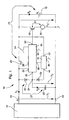
- FIG. 1 shows an accumulator-operated device according to the invention in the form of an electric toothbrush 10 with an accumulator 12 consisting of a cell.
- the electric toothbrush 10 is associated with a mains-powered charging device, which is shown in FIG. 1 merely by means of an electrical energy source designated as supply 14.
- supply 14 an electrical energy source designated as supply 14.
- the network connections and the transmission means between the charging device and toothbrush be it in the form of plug contacts, as in DE-40 22 642, or by means of inductive transmission, as in CH-656 987th
- the supply 14 is at least temporarily substantially as a power source operable, has a correspondingly high-impedance internal resistance and is a load-dependent Charging voltage U1 and a charging current I1 to the toothbrush 10, wherein the charging voltage U1 in the toothbrush between a positive 16 and a negative point 18 is located.
- the charging voltage U1 corresponds to a DC voltage, the course of which may be constant or variable, ie uniform or non-uniform. For example, it may also have a sine half-wave shape.
- the positive point 16 leads to the drain terminal of a MOS field-effect transistor 20 for switching on and off the charging process, whose source terminal continues to lead to the positive terminal of the accumulator 12.
- the negative terminal of the accumulator 12 is connected to the negative point 18 of the feed 14.
- the source-source path of the MOS field-effect transistor 20 forms a series circuit 21 with the accumulator 12.
- the accumulator 12 has a DC voltage, which is designated with battery voltage U3, and corresponds from the perspective of the supply 14 of a low-impedance, first load.
- the positive point 16 is also connected to the anode of a diode 22 whose cathode leads to a node 24.
- a capacitor 26 and the cathode of another diode 28 are connected to this node 24.
- the other terminal of the capacitor 26 is connected to the negative point 18.
- the diode 22 and the capacitor 26 thus form a series circuit designated 27. Over the capacitor 26 or between the node 24 and the negative point 18 is a DC voltage, the capacitor voltage U2 is called.
- the charging or discharging current of the capacitor 26 is denoted by 12.
- control unit 30 is connected via its positive feed input 32 to the node 24, while their negative feed input 34 leads to the negative point 18.
- the control unit 30 has an input 35 which is connected to the positive point 16 and an output 36 which is connected to the gate terminal of the MOS field-effect transistor 20 is connected.
- Another output 38 is connected to a voltage quadrupler 40.
- This voltage quadrupler 40 has, on the one hand, an input 42, which leads to the positive terminal of the accumulator 12, and an output 44, which is connected to the anode of the diode 28.
- the voltage quadrupler 40 is also connected to the negative point 18 via a negative feed input 46.
- a series circuit 51 comprising a MOS field-effect transistor 48 and a motor 50, i. the drain terminal of the MOS field-effect transistor 48 is connected to the positive terminal of the accumulator 12, its source leads to one terminal of the motor 50, and the other terminal of the motor 50 is connected to the negative point 18 of the feeder 14 ,
- I3 The charging or discharging current of the accumulator 12 is denoted by I3.
- the gate terminal of the MOS field-effect transistor 48 leads to an output 52 of the control unit 30. Further, a switch 54 for starting the motor 50 is connected to the control unit 30, which will be referred to below as the motor switch.
- the control unit 30 has various, not shown in the figure 1 components.
- a capacity counter is provided which informs about the state of charge of the accumulator 12.
- two voltage doubler are provided which serve to drive the gates of the two MOS field-effect transistors 20 and 48 and whose outputs correspond to the outputs 36 and 52 of the control unit 30.
- the control unit 30 has a time base which controls the switching and blocking of the MOS field-effect transistor 20.
- the supply internally generates an open-circuit voltage of 9V, but a zener diode not shown in FIG. 1 limits the supply voltage U1 to 6.8V. Since the diode 22 is forward biased, the capacitor 26 is charged so that the capacitor voltage U2 at node 24 rises from 0V to approximately 5V. As a result, the positive supply input 32 is in a short time at a sufficiently high supply voltage and the control unit 30 can take their function.
- the capacitor voltage U2 is more than 0.7V due to the relatively high switching frequency of the MOS field-effect transistor 20 U1 and the capacitance of the diode 22, i. by almost 2V lower than the supply voltage U1, which is assumed to average values.
- the control unit 30 drives the MOS field-effect transistor 20 via the output 36 with a relatively high voltage of about 10V to achieve a low drain-to-source volume resistance R DSon of about 1.5 ohms.
- the compared to the capacitor voltage U2 about twice as high voltage of 10V is generated by the previously mentioned, but not shown voltage doubler of the control unit 30.
- the now conducting MOS field-effect transistor 20 starts the charging process of the accumulator 12, the accumulator charging current I3 of the supply 14 being approximately 200 mA, at the MOS field-effect transistor 20, a voltage drop of about 0.3V is formed and the supply voltage U1 is almost completely torn off. Since the capacitor voltage U2 of the node 24 clearly exceeds the supply voltage U1, the diode 22 is now in reverse polarity and prevents the discharge of the capacitor 26 via the accumulator 12.
- the capacitor 26 feeds the control unit 30 and is thereby discharged, its capacitance being dimensioned so that the capacitor voltage U2 decreases as a function of the present input resistance of the positive feed input 32 only within the permissible range, as can be seen from the U2 curve of FIG is.
- a trouble-free function of the control unit 30 is guaranteed up to a voltage of 1.2V.
- time interval t1 The duty cycle of the MOS field-effect transistor 20 of 200 ms is referred to as time interval t1, as can be seen from FIG.
- time interval t2 The time base of the control unit 30 restricts the charging time of the capacitor 26 to 2 ms. This period is called time interval t2, as can also be seen in FIG.
- control unit 30 controls the MOS field-effect transistor 20 to effect the resumption of the interrupted charging of the accumulator 12 again for the duration of the time interval t1.
- the time interval t1 is to be dimensioned such that the capacitor voltage U2 falls far from the minimum allowable 1.2V. Also, the time interval t2 must be sufficiently large to allow a full charge of the capacitor 26, respectively. With a capacitance of 4uF of the capacitor 26, the critical capacitor voltage U2 is reached only after ten seconds.
- the state of charge of the accumulator 12 is determined indirectly by the control unit 30 by interrogating the state of the capacity counter, which is incremented during loading, and which is decremented during discharge.
- the control unit 30 registers via the input 35 that the supply voltage U1 has been eliminated and starts via the output 38 of the voltage quadrupler 40, which is also referred to as a voltage pump.
- the voltage quadrupler quadruples the accumulator voltage U3 at its input 42 from 1.45V to a voltage of 5.8V, which is supplied via its output 44 to the node 24, i. is delivered to the positive feed input 32 of the control unit 30. This voltage feedback is necessary because the compensation of the discharge of the capacitor 26 through the feed 14, as mentioned, no longer occurs.
- control unit 30 switches the MOS field-effect transistor 48 via the output 52 via the voltage doubler via the output 52, whereby the discharge of the accumulator 12 via the motor 50 starts.
- the voltage quadrupler 40 At an accumulator voltage U3 of 0.7V, the voltage quadrupler 40 generates at its output 44 2.8V, of which 0.7V drop across the diode 28, so that the control unit 30 is supplied with a voltage U2 of about 2.1V.
- the two voltage doublers, not shown, of the control unit 30 At a voltage U2 of 2.1V, the two voltage doublers, not shown, of the control unit 30 generate at the gates of the MOS field-effect transistors 20 and 48 a little more than 4V, whereby still a satisfactorily low drain-source volume resistance R DSon of less than 30hm is ensured.
- the function of the control unit 30 can be maintained up to a rechargeable battery voltage U3 of 0.45V, since the voltage quadrupler in this case at its output 44 still 1.8V of which 0.6V drop across the diode 28, so that the control unit 30 is fed with a minimum allowable voltage of about 1.2V.
- control unit 30 switches off the MOS field-effect transistor 48 automatically after 4 seconds.
- a direct connection between the accumulator 12 and the control unit 30 may be provided so that the latter can monitor the state of charge directly.
- the positive point 16 in FIG. 1 leads to the diode 22
- the point 16 it is also possible for the point 16 to be connected directly to one terminal of the capacitor 26 while its other leads to the anode of the diode 22, the cathode of which is negative Point 18 is connected.
- the load fed by the capacitor, in FIG. 1 the control device 30, is only to be connected in parallel with it, ie. between the positive point 16 and the node arranged between capacitor and diode.
- any accumulator or cell type can be used.
- the solution according to the invention can also be used in the case of an accumulator having a plurality of cells. It is crucial how much the battery in the highly discharged state, the voltage supplied by the charger down voltage and whether this voltage is then sufficient to feed another load reliably. Since the total voltage of several cells in the state of deep discharge can be very small and no longer sufficient for feeding an electronic circuit, the use of the inventive solution is equally advantageous here as well. Since the total voltage of a battery with numerous cells in the state of complete discharge can be zero, the solution according to the invention, regardless of the number of cells, is very advantageous.
Landscapes
- Engineering & Computer Science (AREA)
- Power Engineering (AREA)
- Charge And Discharge Circuits For Batteries Or The Like (AREA)
- Stand-By Power Supply Arrangements (AREA)
- Power Steering Mechanism (AREA)
- Brushes (AREA)
Description
- Die Erfindung betrifft ein mit einem wiederaufladbaren Akkumulator betriebenes Gerät nach dem Oberbegriff des Anspruchs 1.
- Dieses Gerät kann beispielsweise ein netzunabhängig betreibbares Gerät wie etwa ein Zahnpflegegerät, insbesondere eine elektrische Zahnbürste, ein Rasierapparat, ein Haarpflegegerät, ein Telefon, ein Küchenkleingerät, oder dergleichen sein.
- In der DE 40 22 642 ist zum Beispiel eine akkubetriebene elektrische Zahnbürste sowie ein dazugehörendes Ladegerät gezeigt, wobei letzteres Mittel zur symmetrischen Begrenzung der Ausgangswechselspannung aufweist, um die Korrosionsanfälligkeit der Anschlusskontakte zwischen Ladegerät und Zahnbürste herabzusetzen. Die Zahnbürste weist lediglich einen Akkumulator, einen Motor zum Antrieb der Bürste, einen Schalter zum Ein- und Ausschalten des Motors sowie eine Diode auf.
- Bei der CH 656 987 hingegen ist eine kontaktlose Energieübertragung vom ortsfesten Ladegerät zum Handgerät vorgesehen, wobei das Ladegerät eine Speisung zur Erzeugung einer hochfrequenten Wechselspannung aufweist, während das Handgerät wiederum einfach aufgebaut ist und nebst einer Sekundärwicklung und einem Akkumulator lediglich Gleichrichter- und Zenerdioden aufweist.
- Bei beiden Lösungen stellt das Ladegerät der Zahnbürste zur Ladung des Akkumulators eine Spannung zur Verfügung, die sich dem Ladezustand des Akkumulators anpasst, d.h. der Akkumulator zieht die Ladespannung herunter. Die Ladespannung ist umso geringer, je weniger Zellen der Akkumulator aufweist, je niedriger die Nennzellenspannung ist und je stärker der Akkumulator entladen ist. Beispielsweise beträgt die Ladespannung einer bereits geladenen NiCd-Zelle etwa 1.5V, während sie im stark entladenen Zustand unter 0.5V sinken kann.
- Falls die Zahnpflegegeräte der obengenannten Dokumente beispielsweise mit nur einer Akkumulatorzelle ausgerüstet sind, steht beim Laden dementsprechend auch nur eine geringe Spannung zur Verfügung. In beiden Fällen ist also keine Möglichkeit gegeben, nebst dem Akkumulator eine weitere Last, wie beispielsweise eine elektronische Schaltung, mit einer ausreichend hohen und mindestens näherungsweise konstanten Spannung zu versorgen. Beispielsweise ist es kaum möglich, diese Zahnplegegeräte mit einer Ladeanzeigeschaltung zu versehen, da die dazu notwendige Speisespannung während dem Ladevorgang nicht verfügbar ist.
- Der vorliegenden Erfindung liegt daher die Aufgabe zugrunde, insbesondere auch während dem Ladevorgang des Akkumulators zusätzliche Lasten mit einer ausreichend hohen und konstanten Speisespannung zu versorgen.
- Die erfindungsgemässe Lösung dieser Aufgabe ergibt sich aus den Merkmalen des Anspruchs 1.
- Vorteilhafte Ausführungsformen gehen aus den abhängigen Ansprüchen hervor.
- Das erfindungsgemässe Gerät weist gegenüber dem Stand der Technik den Vorteil auf, dass während dem Ladevorgang, nebst dem zu ladenden Akkumulator, der aus der Sicht der Speisung eine niederohmige Last darstellt, eine hochohmige zweite Last mit einer konstanten und genügend hohen Spannung versorgt werden kann.
- Dies wird einerseits dadurch erreicht, dass eine Diode und ein Kondensator eine Serieschaltung bilden, die an der von der Ladevorrichtung abgegebenen Spannung liegt, wobei die Diode in Durchlassrichtung angeordnet ist, und anderseits dadurch, dass ein elektronischer Schalter alternierend für kurze Zeit den Ladevorgang des Akkumulators unterbricht, um die Ladevorrichtung zu entlasten, deren Spannung ansteigen zu lassen und den Kondensator zu laden. Die Diode schützt den Kondensator vor Entladung durch den Akkumulator oder die Ladevorrichtung.
- Die erfindungsgemässe Lösung ermöglicht auf sehr kostengünstige Weise die Stromversorgung einer im Vergleich zum Akkumulator hochohmigeren, weiteren Last. Selbstverständlich können auch mehrere Lasten vom Kondensator gespeist werden. Der Kondensator ist unter anderem derart auszulegen, dass die Spannung während seiner Entladung, d.h. während der Ladeperiode des Akkumulators, nur im zulässigen Rahmen fällt. Weiter kann die Ladezeit des Kondensators und ebenso die Anzahl Ladeperioden pro Zeiteinheit variiert werden. Entsprechende Berechnungen zur Festlegung der Kapazität des Kondensators sowie der Schaltzeiten t1 und t2 gehören zum gewöhnlichen Betätigungsfeld des Fachmannes und brauchen deshalb nicht erläutert werden.
- Die Erfindung ist nachfolgend im Sinne eines nicht ausschliessenden Beispiels anhand einer elektrischen Zahnbürste erläutert, wobei auf die Zeichnungen Bezug genommen wird. Es zeigen:
- Figur 1 ein vereinfachtes, elektrisches Schema einer mit einem wiederaufladbaren Akkumulator betriebenen, elektrischen Zahnbürste gemäss der Erfindung und
- Figur 2 verschiedene Spannungsverläufe der erfindungsgemässen Zahnbürste von Figur 1.
- In Fig. 1 ist ein erfindungsgemässes, Akkumulator-betriebenes Gerät in Form einer elektrischen Zahnbürste 10 mit einem aus einer Zelle bestehenden Akkumulator 12 gezeigt. Der elektrische Zahnbürste 10 ist eine netzgespeiste Ladevorrichtung zugeordnet, die in Figur 1 lediglich durch eine mit Speisung 14 bezeichnete, elektrische Energiequelle dargestellt ist. Nicht dargestellt sind unter anderem die Netzanschlüsse sowie die Übertragungsmittel zwischen Ladevorrichtung und Zahnbürste, sei dies in Form von Steckkontakten, wie in DE-40 22 642, oder mittels induktiver Übertragung, wie in CH-656 987.
- Die Speisung 14 ist mindestens zeitweise im wesentlichen als Stromquelle betreibbar, weist einen entsprechend hochohmigen Innenwiderstand auf und gibt eine lastabhängige Ladespannung U1 sowie einen Ladestrom I1 an die Zahnbürste 10 ab, wobei die Ladespannung U1 in der Zahnbürste zwischen einem positiven 16 und einen negativen Punkt 18 liegt. Die Ladespannung U1 entspricht einer Gleichspannung, deren Verlauf konstant oder variabel sein kann, d.h. gleichförmig oder ungleichförmig. Beispielsweise kann sie auch eine Sinus-Halbwellen-Form aufweisen.
- Der positive Punkt 16 führt auf den Drain-Anschluss eines MOS-Feldeffekt-Transistors 20 zum Ein- und Ausschalten des Ladevorganges, dessen Source-Anschluss weiter auf den positiven Anschluss des Akkumulators 12 führt. Der negative Anschluss des Akkumulators 12 ist mit de negativen Punkt 18 der Speisung 14 verbunden. Die Source-Source-Strecke des MOS-Feldeffekt-Transistors 20 bildet mit dem Akkumulator 12 eine Serieschaltung 21.
- Der Akkumulator 12 weist eine Gleichspannung auf, die mit Akkumulatorspannung U3 bezeichnet ist, und entspricht aus der Sicht der Speisung 14 einer niederohmigen, ersten Last.
- Der positiven Punkt 16 ist ausserdem mit der Anode einer Diode 22 verbunden, dessen Kathode auf einen Knoten 24 führt. Mit diesem Knoten 24 in Verbindung stehen ausserdem der eine Anschluss eines Kondensators 26 sowie die Kathode einer weiteren Diode 28. Der andere Anschluss des Kondensators 26 steht mit dem negativen Punkt 18 in Verbindung. Die Diode 22 und der Kondensator 26 bilden somit eine mit 27 bezeichnete Serieschaltung. Über dem Kondensator 26 bzw. zwischen dem Knoten 24 und dem negativen Punkt 18 liegt eine Gleichspannung, die Kondensatorspannung U2 genannt wird. Der Lade- oder Entladestrom des Kondensators 26 ist mit 12 bezeichnet.
- Weiter ist eine Steuereinheit 30 über ihren positiven Speiseeingang 32 mit dem Knoten 24 verbunden, während ihr negativer Speiseeingang 34 auf den negativen Punkt 18 führt. Die Steuereinheit 30 weist einen Eingang 35 auf, der mit dem positiven Punkt 16 verbunden ist, sowie einen Ausgang 36, der am Gate-Anschluss des MOS-Feldeffekt-Transistors 20 angeschlossen ist. Ein weiterer Ausgang 38 steht mit einem Spannungs-Vervierfacher 40 in Verbindung.
- Dieser Spannungs-Vervierfacher 40 weist einerseits einen Eingang 42 auf, der auf den positiven Anschluss des Akkumulators 12 führt, sowie einen Ausgang 44, welcher an der Anode der Diode 28 angeschlossen ist. Auch der Spannungs-Vervierfacher 40 ist über einen negativen Speiseeingang 46 mit dem negativen Punkt 18 verbunden.
- Parallel zum positiven und zum negativen Anschluss des Akkumulators 12 ist eine Serieschaltung 51 angeordnet, welche einen MOS-Feldeffekt-Transistor 48 und einen Motor 50 umfasst, d.h. der Drain-Anschluss des MOS-Feldeffekt-Transistors 48 ist mit dem positiven Anschluss des Akkumulators 12 verbunden, sein Source-Anschluss führt auf den einen Anschluss des Motors 50 und der andere Anschluss des Motors 50 ist an den negativen Punkt 18 der Speisung 14 angeschlossen. Der Lade- oder Entladestrom des Akkumulators 12 ist mit I3 bezeichnet.
- Der Gate-Anschluss des MOS-Feldeffekt-Transistors 48 führt auf einen Ausgang 52 der Steuereinheit 30. Weiter ist ein Schalter 54 zur Inbetriebnahme des Motors 50 mit der Steuereinheit 30 verbunden, welcher im folgenden Motorschalter genannt wird.
- Die Steuereinheit 30 weist verschiedene, in der Figur 1 nicht dargestellte Komponenten auf. Beispielsweise ist ein Kapazitätszähler vorgesehen, der über den Ladezustand des Akkumulators 12 informiert. Ebenfalls nicht gezeigt sind zwei Spannungs-Verdoppler, die jeweils zur Ansteuerung der Gates der beiden MOS-Feldeffekt-Transistoren 20 und 48 dienen und deren Ausgänge den Ausgängen 36 bzw. 52 der Steuereinheit 30 entsprechen. Weiter verfügt die Steuereinheit 30 über eine Zeitbasis, welche die Durchschaltung und Blockierung des MOS-Feldeffekt-Transistors 20 steuert.
- Die nun folgende Beschreibung der Funktionsweise der erfindungsgemässen Zahnbürste 10 erfolgt in Bezugnahme auf Fig.1 und 2 und bezieht sich auf folgende Aufgangslage, wobei auch hier alle Angaben nur im Sinne eines Beispieles zu verstehen sind:
- Die Zahnbürste 10 befindet sich im Ladegerät,
- der Motorschalter 54 wird nicht betätigt,
- der Akkumulator 12 ist vollständig entladen,
- der Kondensator 26 ist vollständig entladen,
- der MOS-Feldeffekt-Transistor 20 befindet sich im Sperrzustand und
- der MOS-Feldeffekt-Transistor 48 befindet sich im Sperrzustand.
- Die Speisung erzeugt intern eine Leerlaufspannung von 9V, jedoch limitiert eine in Figur 1 nicht dargestellte Zenerdiode die Speisespannung U1 auf 6.8V. Da die Diode 22 in Durchlassrichtung gepolt ist, wird der Kondensator 26 aufgeladen, so dass die Kondensatorspannung U2 am Knoten 24 von 0V bis auf ungefähr 5V ansteigt. Dadurch liegt der positive Speiseeingang 32 in kurzer Zeit an einer ausreichend hohen Speisespannung und die Steuereinheit 30 kann ihre Funktion aufnehmen. Die Kondensatorspannung U2 ist aufgrund der relativ hohen Schaltfrequenz des MOS-Feldeffekt-Transistors 20 U1 und der Kapazität der Diode 22 um mehr als 0.7V, d.h. um fast 2V geringer als die Speisespannung U1, wobei hier von Mittelwerten ausgegangen wird.
- Die Steuereinheit 30 steuert den MOS-Feldeffekt-Transistor 20 über den Ausgang 36 mit einer relativ hohen Spannung von etwa 10V an, um einen geringen Drain-Source-Durchgangswiderstand RDSon von etwa 1.5Ohm zu erzielen. Die gegenüber der Kondensatorspannung U2 ungefähr doppelt so hohe Spannung von 10V wird vom bereits erwähnten, jedoch nicht dargestellten Spannungs-Verdoppler der Steuereinheit 30 erzeugt.
- Solange die Akkumulatorspannung U3 0.7V nicht übersteigt, bleibt eine durch Betätigung des Motorschalters 54 auslösbare Inbetriebnahme des Motors 50 blockiert.
- Der nun leitende MOS-Feldeffekt-Transistor 20 setzt den Ladevorgang des Akkumulators 12 in Gang, wobei der Akkumulator-Ladestrom I3 der Speisung 14 etwa 200mA beträgt, am MOS-Feldeffekt-Transistor 20 ein Spannungsabfall von ungefähr 0.3V entsteht und die Speisespannung U1 nahezu vollständig heruntergerissen wird. Da die Kondensatorspannung U2 des Knotens 24 die Speisespannung U1 deutlich übertrifft, befindet sich die Diode 22 nun in Sperrpolung und verhindert die Entladung des Kondensators 26 über den Akkumulator 12.
- Der Kondensator 26 speist die Steuereinheit 30 und wird dabei entladen, wobei seine Kapazität so bemessen ist, dass die Kondensatorspannung U2 in Abhängigkeit des vorliegenden Eingangswiderstandes des positiven Speiseeinganges 32 nur im zulässigen Rahmen sinkt, wie dies aus dem U2-Verlauf von Fig.2 ersichtlich ist. Eine störfreie Funktion der Steuereinheit 30 ist bis zu einer Spannung von 1.2V gewährleistet.
- Durch die in der Steuereinheit 30 enthaltene Zeitbasis wird der MOS-Feldeffekt-Transistor 20 200ms nach dem Einschalten wieder ausgeschaltet und somit der Ladevorgang des Akkumulators 12 unterbrochen. Die Einschaltdauer des MOS-Feldeffekt-Transistors 20 von 200ms wird mit Zeitintervall t1 bezeichnet, wie es aus der Figur 2 hervorgeht. Durch die Entlastung der Speisung 14 schnellt die Speisespannung U1 zurück auf 6.8V und der Ladevorgang des Kondensators 26 über die Diode 22 setzt erneut ein. Die Zeitbasis der Steuereinheit 30 beschränkt die Ladedauer des Kondensators 26 auf 2ms. Diese Zeitspanne wird Zeitintervall t2 genannt, wie es ebenfalls aus der Figur 2 ersichtlich ist.
- Anschliessend steuert die Steuereinheit 30 den MOS-Feldeffekt-Transistor 20 an, um die Wiederaufnahme des unterbrochenen Ladevorganges des Akkumulators 12 erneut für die Dauer des Zeitintervalles t1 zu bewirken. Nach Ablauf des Zeitintervalles t1 folgt wiederum während der Zeitspanne t2 die Deckung des zwischenzeitlich entstandenen Ladungsverlustes des Kondensators 26.
- Der Ladevorgang des Akkumulators 12 während t1 und der Ladevorgang des Kondensators 26 während t2 wechseln sich fortlaufend ab, wobei Versuche gezeigt haben, dass die kurzen Ladeunterbrüche des Akkumulators 12 keinen negativen Einfluss auf seine Kapazität, die Lebensdauer oder andere Grössen haben.
- Diese periodisch durchgeführte Kompensation der Ladung des Kondensators 12 wird vom Anmelder "refreshing" genannt, da der Ladezustand gewissermassen aufgefrischt wird, und bildet einer der Kernpunkte der vorliegenden Erfindung.
- In der Fig.2 ist der Anstieg der Ladespannung U1 in übertriebenen Mass gezeigt, damit mit zunehmender Akkuspannung U3 deutlich wird, dass die Ladespannung U1 weniger stark heruntergerissen wird.
- Selbstverständlich ist das Zeitintervall t1 derart zu bemessen, dass die Kondensatorspannung U2 bei weitem nicht auf die minimal zulässigen 1.2V fällt. Auch muss das Zeitintervall t2 genügend gross sein, um jeweils eine vollständige Ladung des Kondensators 26 zu ermöglichen. Mit einer Kapazität von 4uF des Kondensators 26 wird die kritische Kondensatorspannung U2 erst nach zehn Sekunden erreicht.
- Der Ladezustand des Akkumulators 12 wird von der Steuereinheit 30 indirekt ermittelt, indem der Zustand des beim Laden inkrementierten beim Entladen dekrementierten Kapazitätszählers abgefragt wird.
- Da die Gefahr besteht, dass der Zustand des Kapazitätszählers nicht genau mit dem tatsächlichen Ladezustand des Akkumulators 12 übereinstimmt, beispielsweise, weil der Benützer den Motor 50 stärker belastet, als ursprünglich angenommen, ist nach jedem Entladevorgang ein leichtes Überladen des Akkumulators 12 vorgesehen. Dieses leichte Überladen wird dadurch erreicht, indem der Kapazitätszähler grundsätzlich immer von einem grossen Entladestrom I3 ausgeht, selbst wenn der Motor 50 kaum belastet wird. Dabei ist der Ladestrom I3 derart bemessen, dass der Akkumulator 12 bei Überladung keinen Schaden nimmt. Ein Ladestrom I3 von 100mA beispielsweise ist durchaus zulässig. Dabei tritt auch kein allmählich auftretender Kapazitätsverlust des Kondensators 12 auf.
- Bis anhin wurde davon ausgegangen, dass sich die elektrische Zahnbürste dauernd im ortsfesten, in Figur 1 nicht dargestellten Ladegerät befindet und die Speisung 14 beispielsweise über einen Transformator mit dem Netz in Energieübertragungs-Verbindung steht.
- Für die folgende Beschreibung wird nun angenommen, dass der Akkumulator 12 bei einer Entnahme der elektrischen Zahnbürste 10 aus dem Ladegerät bereits vollständig geladen ist und sich der MOS-Feldeffekt-Transistor 20 im Sperrzustand befindet. Die Steuereinheit 30 registriert über den Eingang 35, dass die Speisespannung U1 weggefallen ist und setzt über den Ausgang 38 des auch als Spannungspumpe bezeichneten Spannungs-Vervierfachers 40 in Betrieb.
- Der Spannungs-Vervierfacher 40 vervierfacht die an seinem Eingang 42 liegende Akkumulatorspannung U3 von 1.45V auf eine Spannung von 5.8V, welche über seinen Ausgang 44 an den Knoten 24, d.h. an den positiven Speiseeingang 32 der Steuereinheit 30 abgegeben wird. Diese Spannungsrückführung ist notwendig, da die Kompensation der Entladung des Kondensators 26 durch die Speisung 14, wie erwähnt, nicht mehr erfolgt.
- Betätigt der Benützer den Motorschalter 54, schaltet die Steuereinheit 30 mittels des in Figur 1 nicht dargestellten Spannungs-Verdopplers über den Ausgang 52 den MOS-Feldeffekt-Transistor 48 ein, wodurch die Entladung des Akkumulators 12 über den Motor 50 einsetzt.
- Bei einer Akkumulatorspannung U3 von 0.7V erzeugt der Spannungs-Vervierfacher 40 an seinem Ausgang 44 2.8V, von welchen 0.7V über der Diode 28 abfallen, so dass die Steuereinheit 30 mit einer Spannung U2 von etwa 2.1V gespeist wird. Bei einer Spannung U2 von 2.1V erzeugen die beiden nicht gezeigten Spannungs-Verdoppler der Steuereinheit 30 an den Gates der MOS-Feldeffekt-Transistoren 20 und 48 noch etwas mehr als 4V, wodurch immer noch ein zufriedenstellend tiefer Drain-Source-Durchgangswiderstand RDSon von unter 30hm gewährleistet ist.
- Sollte sich die elektrische Zahnbürste 10 während langer Zeit nicht im Ladegerät befinden und die Selbstentladung voranschreiten, kann die Funktion der Steuereinheit 30 bis zu einer Akkumulatorspannung U3 von 0.45V aufrechterhalten werden, da der Spannungs-Vervierfacher in diesem Fall an seinem Ausgang 44 noch 1.8V erzeugt, von welchen 0.6V über der Diode 28 abfallen, so dass die Steuereinheit 30 mit einer kleinstzulässigen Spannung von etwa 1.2V gespeist wird.
- Sollte der Benützer den Motor 50 blockieren, schaltet die Steuereinheit 30 den MOS-Feldeffekt-Transistor 48 nach 4 Sekunden selbsttätig ab.
- Zwecks Begrenzung des Ladestromes I2 des Kondensators 26 kann es sinnvoll sein, in Serie zu letzterem einen Widerstand vorzusehen.
- Allenfalls kann eine direkte Verbindung zwischen dem Akkumulator 12 und der Steuereinheit 30 vorgesehen werden, damit letztere den Ladezustand direkt überwachen kann.
- Selbstverständlich können der Serieschaltung 27 zwischen Kondensator 26 und Diode 22 auch weitere Element hinzugefügt werden, wie etwa ein Widerstand zur Ladestrom-Begrenzung des Kondensators 26.
- Obwohl in Figur 1 der positiven Punkt 16 auf die Diode 22 führt, ist es beispielsweise auch möglich, dass der Punkt 16 direkt mit dem einen Anschluss des Kondensators 26 verbunden ist, während sein anderer auf die Anode der Diode 22 führt, deren Kathode am negativen Punkt 18 angeschlossen ist. Die vom Kondensator gespeiste Last, in Figur 1 die Steuervorrichtung 30, ist lediglich parallel zu diesem anzuschliessen, d.h. zwischen dem positiven Punkt 16 und dem zwischen Kondensator und Diode angeordneten Knoten.
- Grundsätzlich kann neben NiCd auch jede Akkumulator- bzw. Zellensorte verwendet werden.
- Obwohl im gezeigten Beispiel von nur einer Akkuzelle ausgegangen wird, kann die erfindungsgemässe Lösung auch bei einem Akkumulator mit mehreren Zellen eingesetzt werden. Entscheidend ist, wie stark der Akkumulator im stark entladenen Zustand die von der Ladevorrichtung abgegebene Spannung herunterreisst und ob diese Spannung dann noch ausreicht, um eine weitere Last zuverlässig zu speisen. Da die Gesamtspannung von mehreren Zellen im Zustand der Tiefentladung sehr klein sein und zur Speisung eines elektronischen Schaltkreises nicht mehr ausreichen kann, ist der Einsatz der erfindungsgemässen Lösung auch hier gleichermassen vorteilhaft. Da die Gesamtspannung eines Akkumulators mit zahlreichen Zellen im Zustand vollständiger Entladung Null betragen kann, ist die Lösung gemäss der Erfindung unabhängig der Zellenzahl sehr vorteilhaft.
- Von zentraler Bedeutung sind
- die Funktion des Kondensators als Kurzzeit-Energiespeicher,
- die Diode als Mittel zum Schutz vor ungewünschter Entladung des Kondensators und
- das zyklische, kurzzeitige Unterbrechen des Akku-Ladevorganges zwecks Entlastung der einen relativ hohen Innenwiderstand aufweisenden Ladevorrichtung.
Claims (14)
- Akkumulator-betriebenes Gerät (10) mit einem aus mindestens einer Zelle bestehenden Akkumulator (12), wobei- dem Gerät (10) eine Ladevorrichtung mit einer elektrischen Energiequelle (14) zugeordnet ist, die im Gerät (10) zwischen zwei Punkten (16,18) mindestens zeitweise eine lastabhängige Spannung (U1) erzeugt, und- der Akkumulator (12) für die elektrische Energiequelle (14) eine erste Last bildet,dadurch gekennzeichnet,- dass der Akkumulator (12) mit einem ersten Schaltmittel (20) eine erste Serieschaltung (21) bildet, die zwischen den Punkten (16,18) angeordnet ist,- dass ein Gleichrichterelement (22) und ein Kondensator (26) eine zweite Serieschaltung (27) bilden, die ebenfalls zwischen den beiden Punkten (16, 18) angeordnet ist, wobei das Gleichrichterelement (22) in Bezug auf die Spannung (U1) in Durchlassrichtung angeordnet ist und zwischen dem Gleichrichterelement (22) und dem Kondensator (26) ein Knoten (24) definiert ist,- dass eine gegenüber der ersten Last hochohmigere, zweite Last (30) mit dem Knoten (24) und mindestens einem der Punkte (16,18) in Verbindung steht und- dass ein Steuermittel (30) zum zyklischen Schalten des ersten Schaltmittels (20) vorgesehen ist, um alternierend im Einschaltzustand den Ladevorgang des Akkumulators (12) und im Ausschaltzustand den Ladevorgang des Kondensators (26) zu ermöglichen.
- Akkumulator-betriebenes Gerät (10) nach Anspruch 1, dadurch gekennzeichnet, dass die zweite Last (30) eine elektronische Schaltung bildet, deren erster Speiseanschluss (32) mit dem Knoten (24) und deren zweiter Speiseanschluss (34) mit einem ersten (18) der beiden Punkte (16, 18) verbunden ist.
- Akkumulator-betriebenes Gerät (10) nach Anspruch 1 oder 2, dadurch gekennzeichnet,- dass in Bezug auf die Spannung U1 ein erster (18) der Punkte (16,18) ein negatives Potential (-) und ein zweiter (16) dieser Punkte (16,18) ein positives Potential (+) aufweist und- dass das Gleichrichterelement (22) eine Diode umfasst, deren Anode mit dem zweiten Punkt (16) und deren Kathode mit dem Knoten (24) verbunden ist.
- Akkumulator-betriebenes Gerät (10) nach Anspruch 1, 2 oder 3, dadurch gekennzeichnet, dass eine dritte Last (50) mit einem zweiten Schaltmittel (48) eine dritte Serieschaltung (51) bildet, die mit dem Akkumulator (12) verbunden ist.
- Akkumulator-betriebenes Gerät (10) nach Anspruch 4, dadurch gekennzeichnet, dass die dritte Last (50) ein Motor ist.
- Akkumulator-betriebenes Gerät (10) nach einem der vorangehenden Ansprüche, dadurch gekennzeichnet, dass das erste und das zweite Schaltmittel (20, 48) MOS-Feldeffekt-Transistor sind.
- Akkumulator-betriebenes Gerät (10) nach einem der vorangehenden Ansprüche, dadurch gekennzeichnet, dass der Akkumulator (12) nur eine Zelle aufweist.
- Akkumulator-betriebenes Gerät (10) nach einem der vorangehenden Ansprüche, dadurch gekennzeichnet, dass die Ladevorrichtung sowie das Gerät (10) Mittel zur induktiven Übertragung von Energie von der Ladevorrichtung zum Gerät (10) aufweisen.
- Akkumulator-betriebenes Gerät (10) nach einem der vorangehenden Ansprüche, dadurch gekennzeichnet, dass eine Rückführung vom Akkumulator (12) über einen Aufwärtswandler (40) zum Knoten (24) vorgesehen ist.
- Akkumulator-betriebenes Gerät (10) nach einem der vorangehenden Ansprüche, dadurch gekennzeichnet, dass es (10) ein Gerät aus der Gruppe ist, die elektrische Zahnplegegeräte, elektrische Zahnbürsten und elektrische Rasierapparate umfasst.
- Akkumulator-betriebenes Gerät (10) nach einem der vorangehenden Ansprüche, dadurch gekennzeichnet, dass die Spannung (U1) im wesentlichen einen konstanten oder variablen Verlauf aufweist.
- Verfahren für ein Akkumulator-betriebenes Gerät (10) nach einem der vorangehenden Ansprüche, dadurch gekennzeichnet,- dass sich die Spannung (U1) der elektrischen Energiequelle (14) im Einschaltzustand des ersten Schaltmittels (20) dem Ladezustand des Akkumulators (12) anpasst und- dass die Spannung (U1) der elektrischen Energiequelle (14) im Unterbruchszustand des ersten Schaltmittels (20) demgegenüber höher ausfällt und über das Gleichrichterelement (22) den Kondensator (26) ladet.
- Verfahren nach Anspruch 12, dadurch gekennzeichnet, dass die Einschaltdauer (t1) des ersten Schaltmittels (20) die Unterbruchsdauer (t2) um ein Vielfaches übertrifft.
- Verfahren nach Anspruch 13, dadurch gekennzeichnet, dass die Einschaltdauer (t1) des ersten Schaltmittels (20) Bruchteile von Sekunden dauern kann, während die Unterbruchsdauer (t2) nur in der Grössenordnung von Millisekunden liegt.
Priority Applications (5)
| Application Number | Priority Date | Filing Date | Title |
|---|---|---|---|
| AT97107302T ATE357767T1 (de) | 1997-05-02 | 1997-05-02 | Akkumulator-betriebenes gerät |
| DE59712830T DE59712830D1 (de) | 1997-05-02 | 1997-05-02 | Akkumulator-betriebenes Gerät |
| EP97107302A EP0875978B1 (de) | 1997-05-02 | 1997-05-02 | Akkumulator-betriebenes Gerät |
| CA002236433A CA2236433A1 (en) | 1997-05-02 | 1998-04-30 | Battery operated apparatus |
| JP10123586A JPH10322935A (ja) | 1997-05-02 | 1998-05-06 | 電池作動式装置 |
Applications Claiming Priority (1)
| Application Number | Priority Date | Filing Date | Title |
|---|---|---|---|
| EP97107302A EP0875978B1 (de) | 1997-05-02 | 1997-05-02 | Akkumulator-betriebenes Gerät |
Publications (2)
| Publication Number | Publication Date |
|---|---|
| EP0875978A1 EP0875978A1 (de) | 1998-11-04 |
| EP0875978B1 true EP0875978B1 (de) | 2007-03-21 |
Family
ID=8226760
Family Applications (1)
| Application Number | Title | Priority Date | Filing Date |
|---|---|---|---|
| EP97107302A Expired - Lifetime EP0875978B1 (de) | 1997-05-02 | 1997-05-02 | Akkumulator-betriebenes Gerät |
Country Status (5)
| Country | Link |
|---|---|
| EP (1) | EP0875978B1 (de) |
| JP (1) | JPH10322935A (de) |
| AT (1) | ATE357767T1 (de) |
| CA (1) | CA2236433A1 (de) |
| DE (1) | DE59712830D1 (de) |
Cited By (1)
| Publication number | Priority date | Publication date | Assignee | Title |
|---|---|---|---|---|
| EP2571150A2 (de) | 2011-09-16 | 2013-03-20 | Braun GmbH | Stromversorgungsschaltung für ein elektrisches Gerät mit einer Batterie und einem DC/DC-Wandler |
Families Citing this family (1)
| Publication number | Priority date | Publication date | Assignee | Title |
|---|---|---|---|---|
| EP2230744B1 (de) * | 2009-03-19 | 2012-05-16 | Braun GmbH | Schaltungsanordnung und Verfahren zur Ladeerkennung |
Family Cites Families (4)
| Publication number | Priority date | Publication date | Assignee | Title |
|---|---|---|---|---|
| US4220872A (en) * | 1978-12-26 | 1980-09-02 | Gte Sylvania Incorporated | DC power supply circuit |
| DE3108847C2 (de) * | 1981-03-09 | 1983-10-27 | Trisa Bürstenfabrik AG Triengen, 6234 Triengen | Einrichtung zum Laden von Akkumulatoren |
| CA1235178A (en) * | 1984-05-04 | 1988-04-12 | Kiyotaka Mukai | Electrical apparatus connected with a battery charger system |
| JPH04207929A (ja) * | 1990-11-30 | 1992-07-29 | Fujitsu Ltd | 充電器の充放電制御方式 |
-
1997
- 1997-05-02 AT AT97107302T patent/ATE357767T1/de active
- 1997-05-02 DE DE59712830T patent/DE59712830D1/de not_active Expired - Lifetime
- 1997-05-02 EP EP97107302A patent/EP0875978B1/de not_active Expired - Lifetime
-
1998
- 1998-04-30 CA CA002236433A patent/CA2236433A1/en not_active Abandoned
- 1998-05-06 JP JP10123586A patent/JPH10322935A/ja active Pending
Cited By (2)
| Publication number | Priority date | Publication date | Assignee | Title |
|---|---|---|---|---|
| EP2571150A2 (de) | 2011-09-16 | 2013-03-20 | Braun GmbH | Stromversorgungsschaltung für ein elektrisches Gerät mit einer Batterie und einem DC/DC-Wandler |
| US9124118B2 (en) | 2011-09-16 | 2015-09-01 | Braun Gmbh | Circuit for a small electric appliance with an accumulator and method for measuring a charging current |
Also Published As
| Publication number | Publication date |
|---|---|
| CA2236433A1 (en) | 1998-11-02 |
| JPH10322935A (ja) | 1998-12-04 |
| ATE357767T1 (de) | 2007-04-15 |
| EP0875978A1 (de) | 1998-11-04 |
| DE59712830D1 (de) | 2007-05-03 |
Similar Documents
| Publication | Publication Date | Title |
|---|---|---|
| EP0162341B1 (de) | Elektronisches Schaltnetzteil | |
| DE3441323C2 (de) | ||
| DE69326283T2 (de) | Gerät zum Laden eines wiederaufladbaren Akkumulators | |
| DE3321458C2 (de) | ||
| DD148845A5 (de) | Batterieeinheit mit dc zu dc konverter | |
| DE20221047U1 (de) | Micro-Controller für ein serielles Batterieladegerät | |
| EP0593869A1 (de) | Wiederaufladbarer Akku | |
| DE1638085A1 (de) | Verfahren und Vorrichtung zum Schnelladen von elektrischen Batterien | |
| DE1944991C3 (de) | Geregelte Sicherheits-Stromversorgungseinrichtung mit einer Pufferbatterie | |
| WO2009015960A1 (de) | Ladungsverteilung durch ladungsübertragung innerhalb batteriepacks | |
| DE2912509A1 (de) | Batterieladeschaltung | |
| DE69605530T2 (de) | Leistungsversorgungsschaltung mit einem transformator und einem schalter auf der sekundärseite des transformators | |
| DE1588540B2 (de) | Batterieladegeraet zum anschluss an ein wechselstromnetz | |
| EP0030276B1 (de) | Schaltungsanordnung zum Laden einer Batterie | |
| WO2009130061A1 (de) | Energiespeicher | |
| DE102006042745A1 (de) | Ladegerät für Sekundärbatterien | |
| EP0875978A1 (de) | Akkumulator-betriebenes Gerät | |
| WO2007017057A2 (de) | Schaltungsanordnung und verfahren zum konvertieren einer wechselspannung in eine gleichgerichtete spannung | |
| DE112019005894T5 (de) | Batterieladegerät | |
| DE2928503A1 (de) | Verfahren und vorrichtung zur vollund/oder ausgleichsladung von mehrzelligen akkumulaturenbatterien bei bregenzter gesamtspannung | |
| DE1935201C3 (de) | Schaltungsanordnung zum Schnelladen einer elektrischen Batterie | |
| DE3050778C2 (de) | ||
| EP0130411A2 (de) | Elektronisches Schaltnetzteil | |
| DE3045445A1 (de) | Schaltungsanordnung zur strom- und spannungsversorgung bei netzausfall | |
| WO1987005452A1 (fr) | Appareil regenerateur de cellules primaires |
Legal Events
| Date | Code | Title | Description |
|---|---|---|---|
| PUAI | Public reference made under article 153(3) epc to a published international application that has entered the european phase |
Free format text: ORIGINAL CODE: 0009012 |
|
| AK | Designated contracting states |
Kind code of ref document: A1 Designated state(s): AT BE CH DE FR GB IT LI NL |
|
| AX | Request for extension of the european patent |
Free format text: AL;LT;LV;RO;SI |
|
| 17P | Request for examination filed |
Effective date: 19990504 |
|
| AKX | Designation fees paid |
Free format text: AT BE CH DE FR GB IT LI NL |
|
| GRAP | Despatch of communication of intention to grant a patent |
Free format text: ORIGINAL CODE: EPIDOSNIGR1 |
|
| GRAS | Grant fee paid |
Free format text: ORIGINAL CODE: EPIDOSNIGR3 |
|
| GRAA | (expected) grant |
Free format text: ORIGINAL CODE: 0009210 |
|
| AK | Designated contracting states |
Kind code of ref document: B1 Designated state(s): AT BE CH DE FR GB IT LI NL |
|
| REG | Reference to a national code |
Ref country code: GB Ref legal event code: FG4D Free format text: NOT ENGLISH |
|
| REG | Reference to a national code |
Ref country code: CH Ref legal event code: EP |
|
| REF | Corresponds to: |
Ref document number: 59712830 Country of ref document: DE Date of ref document: 20070503 Kind code of ref document: P |
|
| GBT | Gb: translation of ep patent filed (gb section 77(6)(a)/1977) |
Effective date: 20070618 |
|
| REG | Reference to a national code |
Ref country code: CH Ref legal event code: NV Representative=s name: ICB INGENIEURS CONSEILS EN BREVETS SA |
|
| ET | Fr: translation filed | ||
| BERE | Be: lapsed |
Owner name: EM MICROELECTRONIC-MARIN SA Effective date: 20070531 |
|
| PLBE | No opposition filed within time limit |
Free format text: ORIGINAL CODE: 0009261 |
|
| STAA | Information on the status of an ep patent application or granted ep patent |
Free format text: STATUS: NO OPPOSITION FILED WITHIN TIME LIMIT |
|
| 26N | No opposition filed |
Effective date: 20071227 |
|
| PG25 | Lapsed in a contracting state [announced via postgrant information from national office to epo] |
Ref country code: BE Free format text: LAPSE BECAUSE OF NON-PAYMENT OF DUE FEES Effective date: 20070531 |
|
| PGFP | Annual fee paid to national office [announced via postgrant information from national office to epo] |
Ref country code: GB Payment date: 20110503 Year of fee payment: 15 |
|
| GBPC | Gb: european patent ceased through non-payment of renewal fee |
Effective date: 20120502 |
|
| PGFP | Annual fee paid to national office [announced via postgrant information from national office to epo] |
Ref country code: AT Payment date: 20120420 Year of fee payment: 16 |
|
| PG25 | Lapsed in a contracting state [announced via postgrant information from national office to epo] |
Ref country code: GB Free format text: LAPSE BECAUSE OF NON-PAYMENT OF DUE FEES Effective date: 20120502 |
|
| PGFP | Annual fee paid to national office [announced via postgrant information from national office to epo] |
Ref country code: DE Payment date: 20130423 Year of fee payment: 17 Ref country code: CH Payment date: 20130424 Year of fee payment: 17 |
|
| PGFP | Annual fee paid to national office [announced via postgrant information from national office to epo] |
Ref country code: NL Payment date: 20130424 Year of fee payment: 17 Ref country code: FR Payment date: 20130626 Year of fee payment: 17 Ref country code: IT Payment date: 20130423 Year of fee payment: 17 |
|
| REG | Reference to a national code |
Ref country code: DE Ref legal event code: R119 Ref document number: 59712830 Country of ref document: DE |
|
| REG | Reference to a national code |
Ref country code: NL Ref legal event code: V1 Effective date: 20141201 |
|
| REG | Reference to a national code |
Ref country code: CH Ref legal event code: PL |
|
| REG | Reference to a national code |
Ref country code: AT Ref legal event code: MM01 Ref document number: 357767 Country of ref document: AT Kind code of ref document: T Effective date: 20140502 |
|
| PG25 | Lapsed in a contracting state [announced via postgrant information from national office to epo] |
Ref country code: LI Free format text: LAPSE BECAUSE OF NON-PAYMENT OF DUE FEES Effective date: 20140531 Ref country code: CH Free format text: LAPSE BECAUSE OF NON-PAYMENT OF DUE FEES Effective date: 20140531 |
|
| REG | Reference to a national code |
Ref country code: DE Ref legal event code: R119 Ref document number: 59712830 Country of ref document: DE Effective date: 20141202 |
|
| PG25 | Lapsed in a contracting state [announced via postgrant information from national office to epo] |
Ref country code: AT Free format text: LAPSE BECAUSE OF NON-PAYMENT OF DUE FEES Effective date: 20140502 Ref country code: NL Free format text: LAPSE BECAUSE OF NON-PAYMENT OF DUE FEES Effective date: 20141201 |
|
| REG | Reference to a national code |
Ref country code: FR Ref legal event code: ST Effective date: 20150130 |
|
| PG25 | Lapsed in a contracting state [announced via postgrant information from national office to epo] |
Ref country code: DE Free format text: LAPSE BECAUSE OF NON-PAYMENT OF DUE FEES Effective date: 20141202 Ref country code: IT Free format text: LAPSE BECAUSE OF NON-PAYMENT OF DUE FEES Effective date: 20140502 |
|
| PG25 | Lapsed in a contracting state [announced via postgrant information from national office to epo] |
Ref country code: FR Free format text: LAPSE BECAUSE OF NON-PAYMENT OF DUE FEES Effective date: 20140602 |