EP0875735B1 - Interpolation circuit for an incremental encoder - Google Patents
Interpolation circuit for an incremental encoder Download PDFInfo
- Publication number
- EP0875735B1 EP0875735B1 EP98107532A EP98107532A EP0875735B1 EP 0875735 B1 EP0875735 B1 EP 0875735B1 EP 98107532 A EP98107532 A EP 98107532A EP 98107532 A EP98107532 A EP 98107532A EP 0875735 B1 EP0875735 B1 EP 0875735B1
- Authority
- EP
- European Patent Office
- Prior art keywords
- phase
- data
- phase angle
- look
- angle data
- Prior art date
- Legal status (The legal status is an assumption and is not a legal conclusion. Google has not performed a legal analysis and makes no representation as to the accuracy of the status listed.)
- Expired - Lifetime
Links
Images

Classifications
-
- H—ELECTRICITY
- H03—ELECTRONIC CIRCUITRY
- H03M—CODING; DECODING; CODE CONVERSION IN GENERAL
- H03M1/00—Analogue/digital conversion; Digital/analogue conversion
- H03M1/12—Analogue/digital converters
- H03M1/20—Increasing resolution using an n bit system to obtain n + m bits
- H03M1/202—Increasing resolution using an n bit system to obtain n + m bits by interpolation
- H03M1/207—Increasing resolution using an n bit system to obtain n + m bits by interpolation using a digital interpolation circuit
-
- G—PHYSICS
- G01—MEASURING; TESTING
- G01D—MEASURING NOT SPECIALLY ADAPTED FOR A SPECIFIC VARIABLE; ARRANGEMENTS FOR MEASURING TWO OR MORE VARIABLES NOT COVERED IN A SINGLE OTHER SUBCLASS; TARIFF METERING APPARATUS; MEASURING OR TESTING NOT OTHERWISE PROVIDED FOR
- G01D5/00—Mechanical means for transferring the output of a sensing member; Means for converting the output of a sensing member to another variable where the form or nature of the sensing member does not constrain the means for converting; Transducers not specially adapted for a specific variable
- G01D5/12—Mechanical means for transferring the output of a sensing member; Means for converting the output of a sensing member to another variable where the form or nature of the sensing member does not constrain the means for converting; Transducers not specially adapted for a specific variable using electric or magnetic means
- G01D5/244—Mechanical means for transferring the output of a sensing member; Means for converting the output of a sensing member to another variable where the form or nature of the sensing member does not constrain the means for converting; Transducers not specially adapted for a specific variable using electric or magnetic means influencing characteristics of pulses or pulse trains; generating pulses or pulse trains
- G01D5/24409—Interpolation using memories
-
- H—ELECTRICITY
- H03—ELECTRONIC CIRCUITRY
- H03M—CODING; DECODING; CODE CONVERSION IN GENERAL
- H03M1/00—Analogue/digital conversion; Digital/analogue conversion
- H03M1/12—Analogue/digital converters
- H03M1/22—Analogue/digital converters pattern-reading type
- H03M1/24—Analogue/digital converters pattern-reading type using relatively movable reader and disc or strip
- H03M1/28—Analogue/digital converters pattern-reading type using relatively movable reader and disc or strip with non-weighted coding
- H03M1/30—Analogue/digital converters pattern-reading type using relatively movable reader and disc or strip with non-weighted coding incremental
- H03M1/303—Circuits or methods for processing the quadrature signals
Definitions
- This invention relates to an interpolation circuit performing digital interpolation processing to two-phase sinusoidal signals of an encoder, which detects position, angle, velocity, angular velocity and so on, to obtain phase angle data with high resolution.
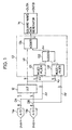
- Fig.4 is an example of the interpolation circuit by previous digital processing.
- Two-phase sinusoidal signals INA and INB of a phase A and a phase B shifted by 90 ° each other are output from an encoder 1, and then sampled with a predetermined frequency by A/D converters 2a and 2b to be converted to digital data DA and DB respectively.
- Phase angle data at each sampling point are prepared and stored in a look-up table memory 3 in advance using an arc tangent function (ATAN) based on the following formula.
- ATAN arc tangent function
- phase angle data u at each sampling point is obtained by reading the look-up table memory 3, defining the digital data DA and DB as addresses x and y respectively. Furthermore, the phase angle data u is entered in a two-phase square wave data generation circuit 4, whereby digital two-phase square wave data OUTA and OUTB are obtained.
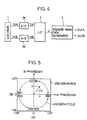
- the memory configuration where the phase angle data obtained by dividing one period into 400 are addressed with the address of 8 bits x 8 bits becomes as Fig.5.
- the published Patent CH 646 784 A5 (Compac Fabrique d' consumes de measure) describes an apparatus for measuring the linear dimensions and the variations of these dimensions by an optical reader and by electronic interpolation.
- An interpolation circuit for an encoder is disclosed in which the phase angle data defined by the high order bits of the digital data obtained by A/D conversion are being interpolated by using the low order bits of these digital data in combination with stored interpolation factors.
- the deviation between the interpolated phase angle obtained in this way and the phase angle data obtained using the look-up table memory having the full address is not always sufficient small.
- the object of the invention is to provide an interpolation circuit for an encoder wherein the phase angle data defined by the high order bits of the digital data obtained by A/D conversion is designed to be interpolated utilizing the low order bits thereof whereby the capacity of the look-up table is reduced and the error between the obtained interpolated phase angle data and the phase angle data obtained by using a look-up table memory with full address is sufficiently small.
- the interpolation circuit of the encoder comprises: an A/D conversion circuit for sampling A-phase and B-phase sinusiodal signals, which are output from an encoder as phase-shifted by 90 ° each other, with a given frequency to convert the resultant to A-phase and B-phase digital data with N bits, respectively; a look-up table memory which stores reference phase angle data corresponding to a plurality of phase divisions and interpolation factors prepared for every phase divisions for interpolating the reference phase data to obtain an interpolated phase angle data, the phase divisions being obtained by dividing a phase space, two-dimensional address of which is assigned by the A-phase and B-phase digital data, to have two-dimensional addresses specified by the high order NU bits data in the A-phase and B-phase digital data, and in which the high order NU bits data is entered as the two-dimensional address signals; and an arithmetic circuit for obtaining the interpolated phase angle data by processing the reference phase angle data and the respective interpolation factor read out from the look-up table memory
- the phase space usually required to a conventional look-up table memory corresponding to a required interpolation number is divided into a plurality of phase divisions.
- the phase angle data corresponding to the number of the phase divisions respectively defined by the high order NU bits of the A-phase and B-phase digital data are stored, and the reference phase angle data is read to be interpolated by the low order NL bits data.
- the interpolation factors used in the interpolation of the phase angle data are stored in the look-up table memory as well as the phase angle data defined by the high order NU bits data.
- the interpolated phase angle data can be obtained by simple interpolation operation in such a manner that the required interpolation number is maintained, while the capacity of the look-up table memory is reduced by a large amount as compared to the case that the look-up table memory has an full address of N ⁇ N and the entire phase angle data defined by this address are stored.
- the two-dimensional address is used for processing the A-phase and B-phase sinusiodal signals, and the phase-interpolating data and the interpolation factor are expressed as two-dimension data
- vector operation is used for interpolation operation.
- an average gradient vector of a change in phase angle data within each small address space as the interpolation factors as well as the reference phase angle data of the reference position of each phase divisions being addressed by the high order NU bits of the A-phase and B-phase digital data are stored in the look-up table memory.
- Fig.1 shows an interpolation circuit of an encoder according to an embodiment of the present invention.
- Fig.2 is a view for illustrating principles of interpolation of phase angle data according to the embodiment.
- Fig.3 is a view for illustrating a relationship between a reference phase angle data and an average gradient vector according to the embodiment.
- Fig.4 shows an interpolation circuit of a prior encoder.
- Fig.5 shows an address and a phase space of a look-up table memory in the interpolation circuit in Fig.4.
- Fig.1 shows an interpolation circuit of an encoder according to an embodiment of the present invention.
- an optical encoder and a magnetic encoder using MR elements are preferably used as the encoder.
- the A-phase and B-phase sinusoidal signals INA and INB output from the encoder are sampled by A/D converters 11a and 11b with a predetermined frequency, respectively, whereby the A-phase and B-phase digital data DA and DB are obtained.
- a look-up table memory 12 constituted by nonvolatile memory such as ROMs is used in order to determine, phase angle.
- the look-up table memory 12 is accesses by the digital data DA and DB.
- This basic configuration is similar to prior art. However, in this embodiment, the phase angle data, number of which is determined by use of predetermined high order bits of the data DA and DB as two-dimensional address signals, are stored in the look-up table memory 12.
- the reference phase angle data u0 corresponding to the respective reference positions (x0, y0) of the respective phase divisions "a" are stored with interpolation factors which are prepared corresponding to the respective reference phase angle data for phase angle interpolating.
- phase divisions "a” are obtained by dividing a phase space, each two-dimensional address of which is assigned by the A-phase and B-phase digital data to have two-dimensional addresses specified by the high order NU bits data in the A-phase and B-phase digital data.
- each of the reference positions of the reference phase angle data u0 is a predetermined position in the respective phase division "a".
- operation for interpolating the phase angle data is performed based on the reference phase angle data and the interpolation factors (i.e., the average gradient vectors) read out from the look-up table memory 12 and the phase-interpolating data corresponding to the low order bits data ⁇ x and ⁇ y.
- Fig.2 shows only the upper right quadrant of the phase space wherein the data DA and DB are represented as addresses x and y.
- u0 is a certain reference phase angle data read out from the look-up table memory 12
- ⁇ u is a vector of the phase-interpolating data defined by the data of NL bits x NL bits that is to be included in the phase division "a”.
- a phase angle data u to be obtained in the case of using the full address of N bits x N bits is obtained by interpolating the reference phase angle data u0 using the vector ⁇ u of the phase-interpolating data.
- the amount of changes (the gradient) in the phase angle data within each phase division "a” is determined by the reference position (x0, y0) of the phase divisions "a", and is substantially uniform. Therefore, as described above, the average gradient vector K of the phase angle data in the phase divisions "a” is determined in advance to be stored as the interpolation factor in the look-up table memory 12 as well as the reference phase angle data u0.
- An interpolated phase angle data u can be obtained by performing a vector inner product operation of the vector ⁇ u of the phase-interpolating data and the average gradient vector K , and by adding the result to the reference phase angle data u0, as represented by the following formula (2).
- u u0 + k x ⁇ u
- x-, y-components of the phase-interpolating data vector ⁇ u are ⁇ x, ⁇ y, respectively.
- x-, y-components of the average gradient vector K are defined as kx, ky, respectively, the formula (2) becomes the following formula (3).
- u u0 + (kx ⁇ ⁇ x + ky ⁇ ⁇ y)
- a first and a second multipliers 131 and 132 multiply the components kx and ky of the average gradient vector K , which are read out from the memory 12, and components ⁇ x and ⁇ y (i.e., components of the phase-interpolating data) represented by the low order NL bits of the digital data DA and DB, respectively.
- a first adder 133 adds the multiplied results of the multipliers 131 and 132.
- the phase-interpolating data vector ⁇ u can be obtained by the adder 133.
- a second adder 134 adds the phase-interpolating data vector ⁇ u to the reference phase angle data u0 read out from the memory 12. As a result an interpolated phase angle data u that is to be required can be obtained.
- the interpolated phase data u is, for example, processed in a two-phase square wave data generation circuit 14 in a conventional manner, whereby two-phase square wave data OUTA and OUTB are output.
- kx and ky of the average gradient vector K in the phase division "a” described above are given by a formula (4) described below, defining a center of the phase division "a” as a typical point (x1, y1) as shown in Figure 3.
- kx - A ⁇ y1/(x1 2 + y1 2 )
- ky +A ⁇ y1/(x1 2 + y1 2 )
- the typical point (x1, y1) determining the average gradient vector K is defined as a center of the phase division "a" in order to improve the accuracy of approximation.
- the reference position (x0, y0) can be selected as a typical point.
- phase angle data u 19 18.37204 18.1047 17.84443 17.59154 18 17.45404 17.19849 16.95013 16.70868 17 16.52854 16.28528 26.04893 15.8192 16 15.59583 15.36517 1 5.1411 14.92337 y/x 64 65 66 67
- TABLE 5 corresponds to the phase angle data being approximately obtained by the interpolation circuit of the embodiment.
- the errors between TABLE 1 and TABLE 5 are summarized as described in the following TABLE 6.
- the errors of the approximate value obtained by the interpolation circuit of the embodiment are such small as less than ⁇ 1 LSB of the number of interpolation 400.
- Nonvolatile memories as ROM, EPROM and EEPROM, and PLD, RAM or the like can be used as the look-up table memory 12 shown in Fig.1.
- the arithmetic circuit 13 performing interpolation operation can be realized through software by a microprocessor or by a DSP except the digital circuit.
- the phase angle data designated by the high order NU bits of the digital data obtained by converting output of the encoder by A/D converter and the average gradient vector of the changes in the phase angle data determined in advance in response to the phase position of the reference phase angle data are stored.
- the interpolation operation is performed based on the data of the low order NL bits, and the reference phase angle data and the average gradient vector read from the look-up table memory, whereby the capacity of the look-up table memory can be largely compressed.
Description
- This invention relates to an interpolation circuit performing digital interpolation processing to two-phase sinusoidal signals of an encoder, which detects position, angle, velocity, angular velocity and so on, to obtain phase angle data with high resolution.
- Since there is a machining limit in grid spaces formed in a scale of the encoder, a space period of the sinusoidal signals from the encoder should be subdivided to be interpolated in order to measure a space finer than the scale grid. Therefore, various interpolation circuits have been used previously.
- Fig.4 is an example of the interpolation circuit by previous digital processing. Two-phase sinusoidal signals INA and INB of a phase A and a phase B shifted by 90 ° each other are output from an encoder 1, and then sampled with a predetermined frequency by A/D converters 2a and 2b to be converted to digital data DA and DB respectively. Phase angle data at each sampling point are prepared and stored in a look-up table memory 3 in advance using an arc tangent function (ATAN) based on the following formula.
- Therefore, the phase angle data u at each sampling point is obtained by reading the look-up table memory 3, defining the digital data DA and DB as addresses x and y respectively. Furthermore, the phase angle data u is entered in a two-phase square wave data generation circuit 4, whereby digital two-phase square wave data OUTA and OUTB are obtained.
- When intending to obtain a sufficient interpolation number in the interpolation circuit in which the look-up table memory is used as described above, capacity of the look-up table memory becomes extremely large. For example, when the digital data DA and DB obtained by A/D converters 2a and 2b are N bits, the size of the address space specified by the digital data DA and DB is N × N. When a required interpolation number is defined as I, the integer J beyond log2 I is required to the phase angle data. In such a condition, the memory capacity required in the look-up table memory becomes 2 2 N × J.
- For example, the memory configuration where the phase angle data obtained by dividing one period into 400 are addressed with the address of 8 bits x 8 bits becomes as Fig.5. When a data length is defined as J = 9, the memory capacity becomes 28 x 28 x 9 = 589,824 bits.
- As a method for reducing the capacity of the look-up table memory in the encoder interpolation circuit of a digital system as described above, a method for reducing the address space have been proposed, paying attention to the symmetry that the phase angle data is repeated periodically within an address space with exception of a sign (Japanese Laid-open Patent Publication No.Hei.3-68812).
- The published Patent CH 646 784 A5 (Compac Fabrique d'appareils de mesure) describes an apparatus for measuring the linear dimensions and the variations of these dimensions by an optical reader and by electronic interpolation. An interpolation circuit for an encoder is disclosed in which the phase angle data defined by the high order bits of the digital data obtained by A/D conversion are being interpolated by using the low order bits of these digital data in combination with stored interpolation factors. However, the deviation between the interpolated phase angle obtained in this way and the phase angle data obtained using the look-up table memory having the full address is not always sufficient small.
- The object of the invention is to provide an interpolation circuit for an encoder wherein the phase angle data defined by the high order bits of the digital data obtained by A/D conversion is designed to be interpolated utilizing the low order bits thereof whereby the capacity of the look-up table is reduced and the error between the obtained interpolated phase angle data and the phase angle data obtained by using a look-up table memory with full address is sufficiently small.
- The object of the invention is achieved by the interpolation circuit according to claim 1. Other embodiments of the invention are described in the dependent claims.
- The interpolation circuit of the encoder according to the present invention comprises: an A/D conversion circuit for sampling A-phase and B-phase sinusiodal signals, which are output from an encoder as phase-shifted by 90 ° each other, with a given frequency to convert the resultant to A-phase and B-phase digital data with N bits, respectively; a look-up table memory which stores reference phase angle data corresponding to a plurality of phase divisions and interpolation factors prepared for every phase divisions for interpolating the reference phase data to obtain an interpolated phase angle data, the phase divisions being obtained by dividing a phase space, two-dimensional address of which is assigned by the A-phase and B-phase digital data, to have two-dimensional addresses specified by the high order NU bits data in the A-phase and B-phase digital data, and in which the high order NU bits data is entered as the two-dimensional address signals; and an arithmetic circuit for obtaining the interpolated phase angle data by processing the reference phase angle data and the respective interpolation factor read out from the look-up table memory and a phase-interpolating data represented by the low order NL (=N-NU) bits data in the A-phase and B-phase digital data.
- In the present invention, the phase space usually required to a conventional look-up table memory corresponding to a required interpolation number is divided into a plurality of phase divisions. In the look-up table memory in the present invention, the phase angle data corresponding to the number of the phase divisions respectively defined by the high order NU bits of the A-phase and B-phase digital data are stored, and the reference phase angle data is read to be interpolated by the low order NL bits data. The interpolation factors used in the interpolation of the phase angle data are stored in the look-up table memory as well as the phase angle data defined by the high order NU bits data. Therefore, the interpolated phase angle data can be obtained by simple interpolation operation in such a manner that the required interpolation number is maintained, while the capacity of the look-up table memory is reduced by a large amount as compared to the case that the look-up table memory has an full address of N × N and the entire phase angle data defined by this address are stored.
- Concretely, since the two-dimensional address is used for processing the A-phase and B-phase sinusiodal signals, and the phase-interpolating data and the interpolation factor are expressed as two-dimension data, vector operation is used for interpolation operation. In the present invention, an average gradient vector of a change in phase angle data within each small address space as the interpolation factors as well as the reference phase angle data of the reference position of each phase divisions being addressed by the high order NU bits of the A-phase and B-phase digital data are stored in the look-up table memory. In this case, such an interpolation operation is performed that a vector inner product of the phase-interpolating data composed of the low order NL bits of the A-phase and B-phase digital data and the average gradient vector read from the look-up table memory is produced, and then the resultant is added to the reference phase angle data read from the look-up table memory. As a result, a deviation (an error) of the phase angle data interpolated according to the present invention from the phase angle data which is obtained when using the look-up table memory having the full address becomes sufficiently small.
- The embodiments according to the present invention will be described referring to the following drawings.
- Fig.1 shows an interpolation circuit of an encoder according to an embodiment of the present invention.
- Fig.2 is a view for illustrating principles of interpolation of phase angle data according to the embodiment.
- Fig.3 is a view for illustrating a relationship between a reference phase angle data and an average gradient vector according to the embodiment.
- Fig.4 shows an interpolation circuit of a prior encoder.
- Fig.5 shows an address and a phase space of a look-up table memory in the interpolation circuit in Fig.4.
- Fig.1 shows an interpolation circuit of an encoder according to an embodiment of the present invention. Although it is no matter what principle is used for the encoder to which the interpolation circuit is applied, an optical encoder and a magnetic encoder using MR elements are preferably used as the encoder. The A-phase and B-phase sinusoidal signals INA and INB output from the encoder are sampled by A/D converters 11a and 11b with a predetermined frequency, respectively, whereby the A-phase and B-phase digital data DA and DB are obtained. A look-up table memory 12 constituted by nonvolatile memory such as ROMs is used in order to determine, phase angle. The look-up table memory 12 is accesses by the digital data DA and DB. This basic configuration is similar to prior art. However, in this embodiment, the phase angle data, number of which is determined by use of predetermined high order bits of the data DA and DB as two-dimensional address signals, are stored in the look-up table memory 12.
- Namely, in the case of the embodiment, the data DA and DB are N bits (N = 8 in Fig.1), respectively. The high order NU bits (NU = 5 in Fig.1) of these data DA and DB are entered into the look-up table memory 12 as two-dimensional address signals. In the memory 12, the reference phase angle data u0 corresponding to the respective reference positions (x0, y0) of the respective phase divisions "a" are stored with interpolation factors which are prepared corresponding to the respective reference phase angle data for phase angle interpolating. The phase divisions "a" are obtained by dividing a phase space, each two-dimensional address of which is assigned by the A-phase and B-phase digital data to have two-dimensional addresses specified by the high order NU bits data in the A-phase and B-phase digital data. The size of each phase division "a" is NL x NL required to store the phase angle data of 22 N L words (64 words in the case of NL = 3) in the case of using the digital data DA and DB of N bits as the full address, as shown in Fig.3.
- As is described below, average gradient vector data of the changes in the phase angle data within the respective phase divisions "a" are used as the interpolation factors being stored as well as the reference phase angle data u0. It is appreciated that each of the reference positions of the reference phase angle data u0 is a predetermined position in the respective phase division "a".
- Data Δ x and Δ y of the low order NL bits (NL = 3 in Fig.1) of the respective data DA and DB are entered into an arithmetic circuit 13 for performing interpolation operation as phase-interpolating data, respectively. In the arithmetic circuit 13, operation for interpolating the phase angle data is performed based on the reference phase angle data and the interpolation factors (i.e., the average gradient vectors) read out from the look-up table memory 12 and the phase-interpolating data corresponding to the low order bits data Δ x and Δ y.
- Referring to Fig.2, the principle of interpolation of phase angle data according to this embodiment will be described. Fig.2 shows only the upper right quadrant of the phase space wherein the data DA and DB are represented as addresses x and y. In Fig.2, u0 is a certain reference phase angle data read out from the look-up table memory 12, and Δ u is a vector of the phase-interpolating data defined by the data of NL bits x NL bits that is to be included in the phase division "a". A phase angle data u to be obtained in the case of using the full address of N bits x N bits is obtained by interpolating the reference phase angle data u0 using the vector Δ u of the phase-interpolating data. The amount of changes (the gradient) in the phase angle data within each phase division "a" is determined by the reference position (x0, y0) of the phase divisions "a", and is substantially uniform. Therefore, as described above, the average gradient vector K of the phase angle data in the phase divisions "a" is determined in advance to be stored as the interpolation factor in the look-up table memory 12 as well as the reference phase angle data u0. An interpolated phase angle data u can be obtained by performing a vector inner product operation of the vector Δ u of the phase-interpolating data and the average gradient vector K , and by adding the result to the reference phase angle data u0, as represented by the following formula (2).
- x-, y-components of the phase-interpolating data vector Δ u are Δ x, Δ y, respectively. When x-, y-components of the average gradient vector K are defined as kx, ky, respectively, the formula (2) becomes the following formula (3).
- The interpolation operation using the vector inner product described above is performed in the arithmetic circuit 13 in Fig. 1. A first and a second multipliers 131 and 132 multiply the components kx and ky of the average gradient vector K , which are read out from the memory 12, and components Δ x and Δ y (i.e., components of the phase-interpolating data) represented by the low order NL bits of the digital data DA and DB, respectively. A first adder 133 adds the multiplied results of the multipliers 131 and 132. The phase-interpolating data vector Δ u can be obtained by the adder 133. A second adder 134 adds the phase-interpolating data vector Δ u to the reference phase angle data u0 read out from the memory 12. As a result an interpolated phase angle data u that is to be required can be obtained.
- The interpolated phase data u is, for example, processed in a two-phase square wave data generation circuit 14 in a conventional manner, whereby two-phase square wave data OUTA and OUTB are output.
- For example, the components kx and ky of the average gradient vector K in the phase division "a" described above are given by a formula (4) described below, defining a center of the phase division "a" as a typical point (x1, y1) as shown in Figure 3.
- In formula (4), when the number of interpolation is defined as I, "A" is: A = I/2 π . The formula (4) is introduced using a mathematical formula of a scalar field. That is, when data represented by the scalar field having a certain spatial distribution of the changes is defined as u = A·, and x-, y-components of a change portion vector Δ u of the data are defined as Δ x, Δ y, respectively, "u" can be given by the following partial differential equation (5).
- Based on the mathematical formula, when the data to be stored in the memory is defined as A = I/2 π (I is defined as the number of interpolation), the components of the average gradient vector of the formula (4) are obtained.
- As is described in Fig. 3, it is preferable that the typical point (x1, y1) determining the average gradient vector K is defined as a center of the phase division "a" in order to improve the accuracy of approximation. However, since the changes within the phase division are small, a large approximation error can not be occurred even when other typical points are selected. For example, the reference position (x0, y0) can be selected as a typical point.
- Moreover, as the other simple method determining the average gradient vector of the changes in the phase angle data, for example, the average gradient vector can be obtained by calculating a difference between two typical points of adjacent phase divisions as follows.
- It will be described that the approximation error of interpolation of the phase angle data using the aforementioned average gradient vector K is small, concretely providing the examples of numeral calculations.
- When the number of interpolation I is 400, the phase angle data u at several positions y/x (= DB/DA) in a range in which the signal amplitude becomes approximately one-half of the minimum, is determined as described in the following Table 1.
Phase angle data u 19 18.37204 18.1047 17.84443 17.59154 18 17.45404 17.19849 16.95013 16.70868 17 16.52854 16.28528 26.04893 15.8192 16 15.59583 15.36517 1 5.1411 14.92337 y/x 64 65 66 67 - In TABLE 1, when the difference data Δ u is determined, defining (x, y) = (64, 16) as the reference position, resulting in as Table 2.
Difference data Δ u 19 2.776216 2.508671 2.248604 1.995715 18 1.858216 1.602661 1.354306 1.112858 17 0.932709 0.689453 0.453103 0.223374 16 0 -0.23066 -0.45472 -0.67246 y/x 64 65 66 67 - Next, when partial differential quotients δ u/ δ x and δ u/ δ y of each phase angle (these quotients correspond to the gradient vector components kx and ky) are determined from the phase angle data u of the TABLE 1, resulting in as TABLE 3 and Table 4 described below.
δ u/ δ x 19 -0.27139 -0.26375 -0.25643 -0.24940 18 -0.25926 -0.25190 -0.24485 -0.23809 17 -0.24681 -0.23975 -0.23299 -0.22651 16 -0.23405 -0.22731 -0.22086 -0.21467 y/x 64 65 66 67 δu/δy 19 0.91415 0.90232 0.89075 0.87945 18 0.92180 0.90966 0.89780 0.88621 17 0.92916 0.91671 0.90456 0.89271 16 0.93621 0.92346 0.91103 0.89892 y/x 64 65 66 67 - The interpolated phase angle data u = u0 + kx· Δ x + ky· Δ y is determined by using the reference phase angle u0 of y/x = 16/64, using the partial differential quotients δ u/ δ x = - 0.24238 and δ u/ δ y = 0.907181 in xl = 65.5, y1 = 17.5 as the average gradient vector components kx and ky from TABLE 3 and TABLE 4, resulting in as TABLE 5 described below.
u = u0 + kx· Δ x + ky· Δ y 19 18.31737 18.07499 17.83262 17.59024 18 17.41019 17.16781 16.92544 16.68306 17 16.50301 16.26063 16.01825 15.77588 16 15.59583 15.35345 15.11107 14.8687 y/x 64 65 66 67 - The results of the TABLE 5 correspond to the phase angle data being approximately obtained by the interpolation circuit of the embodiment. The errors between TABLE 1 and TABLE 5 are summarized as described in the following TABLE 6.
Error 19 -0.05467 -0.02950 -0.01181 -0.00130 18 -0.04385 -0.03067 -0.02470 -0.02563 17 -0.02553 -0.02467 -0.03067 -0.04332 16 -0.00000 -0.01172 -0.03003 -0.05467 y/x 64 65 66 67 - From the numeral data described above, the errors of the approximate value obtained by the interpolation circuit of the embodiment are such small as less than ± 1 LSB of the number of interpolation 400.
- As is described above, when the phase angle data of the number of interpolation 400 was assigned in the look-up table memory being addressed by the address of 8 bits x 8 bits, the memory capacity was 2 8 x 2 8 x 9 = 589,824, defining a data length of the phase angle data as 9. In contrast with this, in case of the embodiment, assuming that the reference phase angle with the same data length and the gradient vector components kx and ky of 5 bits respectively are stored in the look-up table designated by the high order bit of 5 bits x 5 bits, the memory capacity becomes 25 x 2 5 x (9 + 5 + 5) = 19,456 bits. Namely, the memory capacity can be compressed to one thirtieth in comparison with the above-described example.
- Such Nonvolatile memories as ROM, EPROM and EEPROM, and PLD, RAM or the like can be used as the look-up table memory 12 shown in Fig.1. Moreover, the arithmetic circuit 13 performing interpolation operation can be realized through software by a microprocessor or by a DSP except the digital circuit.
- According to the present invention, in the look-up table memory for interpolating, the phase angle data designated by the high order NU bits of the digital data obtained by converting output of the encoder by A/D converter and the average gradient vector of the changes in the phase angle data determined in advance in response to the phase position of the reference phase angle data are stored. The interpolation operation is performed based on the data of the low order NL bits, and the reference phase angle data and the average gradient vector read from the look-up table memory, whereby the capacity of the look-up table memory can be largely compressed.
Claims (5)
- An interpolation circuit for an encoder, comprising:characterized in thatan A/D conversion circuit (11) for sampling A-phase and B-phase sinusoidal signals, which are output from an encoder as phase-shifted by 90° from each other, with a given frequency to convert the resultant to A-phase and B-phase digital data with N bits, respectively;a look-up table memory (12) which stores reference phase angle data corresponding to a plurality of phase angle divisions and interpolation factors prepared for every phase division for interpolating the reference phase angle data to obtain an interpolated phase angle data, the phase angle divisions being obtained by dividing a phase space, a two-dimensional address of which is assigned by the A-phase and B-phase digital data, to have two-dimensional addresses specified by the high order NU bits data in the A-phase and B-phase digital data, and in which the high order NU bits data are entered as the two-dimensional address signals; andan arithmetic circuit (13) for obtaining the interpolated phase angle data by processing the reference phase angle data and the interpolation factors read out from the look-up table memory and a phase-interpolating data represented by the low order NL (=N-NU) bits data in the A-phase and B-phase digital data,
the interpolation factors stored in the look-up table memory are average gradient vectors of changes of the phase angle data predetermined in response to phase positions of the phase division. - The interpolation circuit according to claim 1, wherein the arithmetic circuit comprises:multiplication means (131, 132) for determining a vector inner product of the phase-interpolating data and the average gradient vector read out form the look-up table memory; andaddition means (133, 134) for adding the vector inner product determined by the multiplication means to the reference phase angle data read out from the look-up table memory to output the interpolated phase angle data.
- The interpolation circuit according to claim 1, wherein the arithmetic circuit comprises:first and second multiplication means (131, 132) for performing multiplication of kx · Δx and ky · Δy, respectively, where Δx, Δy are x-, y-components of the phase-interpolating data, respectively, and kx, ky are x-, y-components of the average gradient vector read out from the look-up table memory, respectively;first addition means (133) for adding the results obtained by the first and second multiplication means; andsecond addition means (134) for adding the result added by the first addition means to the reference phase angle data read out from the look-up table memory.
- The interpolation circuit according to claim 1, wherein x-, y-components of the average gradient vector are obtained as partial differential quotients of the phase angle data at a center point within the respective phase division.
- The interpolation circuit according to claim 1, wherein x-, y-components of the average gradient vector are obtained as differentiated values between two typical points in the respective phase division and another phase division adjacent thereto.
Applications Claiming Priority (3)
| Application Number | Priority Date | Filing Date | Title |
|---|---|---|---|
| JP11112397 | 1997-04-28 | ||
| JP11112397A JP3220411B2 (en) | 1997-04-28 | 1997-04-28 | Interpolation circuit of encoder |
| JP111123/97 | 1997-04-28 |
Publications (2)
| Publication Number | Publication Date |
|---|---|
| EP0875735A1 EP0875735A1 (en) | 1998-11-04 |
| EP0875735B1 true EP0875735B1 (en) | 2003-12-10 |
Family
ID=14553027
Family Applications (1)
| Application Number | Title | Priority Date | Filing Date |
|---|---|---|---|
| EP98107532A Expired - Lifetime EP0875735B1 (en) | 1997-04-28 | 1998-04-24 | Interpolation circuit for an incremental encoder |
Country Status (5)
| Country | Link |
|---|---|
| US (1) | US5999113A (en) |
| EP (1) | EP0875735B1 (en) |
| JP (1) | JP3220411B2 (en) |
| CN (2) | CN1306709C (en) |
| DE (1) | DE69820330T2 (en) |
Families Citing this family (18)
| Publication number | Priority date | Publication date | Assignee | Title |
|---|---|---|---|---|
| US6735607B2 (en) | 2001-06-02 | 2004-05-11 | Lockheed Martin Corporation | Transparent data access and interpolation apparatus and method therefor |
| ATE320111T1 (en) * | 2002-01-11 | 2006-03-15 | Heidenhain Gmbh Dr Johannes | METHOD FOR INTERPOLATION OF AT LEAST TWO POSITION-DEPENDENT, PERIODIC, PHASE-SHIFTED ANALOG SIGNALS |
| KR20030085269A (en) * | 2002-04-30 | 2003-11-05 | 전자부품연구원 | Apparatus and method for controlling phase |
| DE10392675B4 (en) * | 2003-04-11 | 2006-10-12 | Mitsubishi Denki K.K. | rotary encoder |
| WO2005013105A1 (en) | 2003-08-04 | 2005-02-10 | Fujitsu Limited | Lookup table and data acquisition method |
| TW200535634A (en) * | 2004-04-20 | 2005-11-01 | Benq Corp | Interpolation method and apparatus of the same |
| DE102004033990B3 (en) * | 2004-07-14 | 2006-04-13 | Siemens Ag | Evaluation method for an analog first signal and an analog second signal as well as corresponding evaluation circuit |
| EP1752740B1 (en) * | 2005-08-11 | 2008-12-03 | Mitutoyo Corporation | Method and Circuit for interpolating an Encoder Output |
| KR100788673B1 (en) | 2005-11-17 | 2007-12-26 | 삼성전자주식회사 | Method and apparatus for processing analog encoder signals |
| JP4746427B2 (en) * | 2005-12-27 | 2011-08-10 | オリンパス株式会社 | Encoder interpolation device |
| EP1979704B1 (en) * | 2006-02-03 | 2017-08-30 | Moog Inc. | Encoder signal analysis system for high-resolution position measurement |
| US8374234B2 (en) | 2006-09-29 | 2013-02-12 | Francis S. J. Munoz | Digital scaling |
| US8418778B2 (en) | 2010-01-07 | 2013-04-16 | Black & Decker Inc. | Power screwdriver having rotary input control |
| US9722334B2 (en) | 2010-04-07 | 2017-08-01 | Black & Decker Inc. | Power tool with light unit |
| US8384014B2 (en) * | 2010-10-27 | 2013-02-26 | Avago Technologies Ecbu Ip (Singapore) Pte. Ltd. | Interpolation method and device for increasing the resolution of encoders |
| US8841600B2 (en) | 2010-10-31 | 2014-09-23 | Avago Technologies General Ip (Singapore) Pte. Ltd. | Hysteresis-compensating interpolation circuits in optical encoders |
| EP2697610A4 (en) * | 2011-04-15 | 2014-11-05 | Yei Corp | Sensor devices utilizing look-up tables for error correction and methods thereof |
| CN114866100B (en) * | 2022-04-28 | 2024-04-12 | 上海航天电子通讯设备研究所 | High-speed automatic gain control system based on phase coding |
Family Cites Families (7)
| Publication number | Priority date | Publication date | Assignee | Title |
|---|---|---|---|---|
| CH646784A5 (en) * | 1982-02-08 | 1984-12-14 | Compac | Device for measuring linear dimensions or variations in these dimensions using an optical reader, and with electronic interpolation |
| JP2501227B2 (en) * | 1988-05-30 | 1996-05-29 | ファナック株式会社 | Absolute position encoder |
| CA2017529A1 (en) * | 1989-06-15 | 1990-12-15 | Michael J. Wax | Prevention of ammonia generation in animal areas |
| EP0408799B1 (en) * | 1989-07-21 | 1993-04-14 | Dr. Johannes Heidenhain GmbH | Method of interpolating position measurement signals |
| US5191336A (en) * | 1991-08-29 | 1993-03-02 | Hewlett-Packard Company | Digital time interpolation system |
| JP3007268B2 (en) * | 1994-06-16 | 2000-02-07 | アンリツ株式会社 | Sawtooth wave generator and signal interpolation device using the same |
| JP3367260B2 (en) * | 1995-03-24 | 2003-01-14 | 三菱電機株式会社 | Encoder device and servo motor control device |
-
1997
- 1997-04-28 JP JP11112397A patent/JP3220411B2/en not_active Expired - Fee Related
-
1998
- 1998-04-14 US US09/059,338 patent/US5999113A/en not_active Expired - Lifetime
- 1998-04-24 DE DE69820330T patent/DE69820330T2/en not_active Expired - Lifetime
- 1998-04-24 EP EP98107532A patent/EP0875735B1/en not_active Expired - Lifetime
- 1998-04-28 CN CNB021605505A patent/CN1306709C/en not_active Expired - Lifetime
- 1998-04-28 CN CN98107930.XA patent/CN1202765A/en active Pending
Also Published As
| Publication number | Publication date |
|---|---|
| US5999113A (en) | 1999-12-07 |
| DE69820330D1 (en) | 2004-01-22 |
| JP3220411B2 (en) | 2001-10-22 |
| CN1516342A (en) | 2004-07-28 |
| JPH10300517A (en) | 1998-11-13 |
| EP0875735A1 (en) | 1998-11-04 |
| CN1306709C (en) | 2007-03-21 |
| CN1202765A (en) | 1998-12-23 |
| DE69820330T2 (en) | 2004-10-21 |
Similar Documents
| Publication | Publication Date | Title |
|---|---|---|
| EP0875735B1 (en) | Interpolation circuit for an incremental encoder | |
| EP0874223B1 (en) | Interpolation circuit for encoder | |
| EP0704678B1 (en) | Method of and apparatus for detecting an amount of displacement | |
| US5907298A (en) | Interpolation circuit for encoder | |
| EP0787973B1 (en) | Method and apparatus for processing angular data from encoder | |
| EP0724137B1 (en) | Interpolation device | |
| US5625310A (en) | Signal processing apparatus and displacement detecting apparatus using the same | |
| US5216626A (en) | Position measuring apparatus and method having reduced memory requirements | |
| JP4746427B2 (en) | Encoder interpolation device | |
| US5506579A (en) | Absolute encoder using multiphase analog signals | |
| JPH0524445B2 (en) | ||
| US6094307A (en) | Optical grating and encoder | |
| JPH08201111A (en) | Interpolation apparatus | |
| EP0940909B1 (en) | Digital FM demodulation circuit | |
| JP3336396B2 (en) | Absolute encoder | |
| JPH08201110A (en) | Interpolation apparatus | |
| EP0455984A1 (en) | Coordinate measuring machine with improved interpolation circuit | |
| Lygouras | Memory reduction in look-up tables for fast symmetric function generators | |
| JP3047946B2 (en) | Angular position signal generator for sine and cosine signals | |
| JPH07139967A (en) | Signal processing circuit of encoder | |
| JPH0244373B2 (en) | ||
| JPH02186221A (en) | Interpolation apparatus of encoder | |
| JPH1151698A (en) | Encoder inserter | |
| JPH04232814A (en) | High-resolution absolute value encoder | |
| JP2001330475A (en) | Encoder |
Legal Events
| Date | Code | Title | Description |
|---|---|---|---|
| PUAI | Public reference made under article 153(3) epc to a published international application that has entered the european phase |
Free format text: ORIGINAL CODE: 0009012 |
|
| AK | Designated contracting states |
Kind code of ref document: A1 Designated state(s): DE FR GB |
|
| AX | Request for extension of the european patent |
Free format text: AL;LT;LV;MK;RO;SI |
|
| 17P | Request for examination filed |
Effective date: 19990323 |
|
| AKX | Designation fees paid |
Free format text: DE FR GB |
|
| 17Q | First examination report despatched |
Effective date: 20030120 |
|
| GRAH | Despatch of communication of intention to grant a patent |
Free format text: ORIGINAL CODE: EPIDOS IGRA |
|
| GRAS | Grant fee paid |
Free format text: ORIGINAL CODE: EPIDOSNIGR3 |
|
| GRAA | (expected) grant |
Free format text: ORIGINAL CODE: 0009210 |
|
| AK | Designated contracting states |
Kind code of ref document: B1 Designated state(s): DE FR GB |
|
| REG | Reference to a national code |
Ref country code: GB Ref legal event code: FG4D |
|
| REF | Corresponds to: |
Ref document number: 69820330 Country of ref document: DE Date of ref document: 20040122 Kind code of ref document: P |
|
| ET | Fr: translation filed | ||
| PLBE | No opposition filed within time limit |
Free format text: ORIGINAL CODE: 0009261 |
|
| STAA | Information on the status of an ep patent application or granted ep patent |
Free format text: STATUS: NO OPPOSITION FILED WITHIN TIME LIMIT |
|
| 26N | No opposition filed |
Effective date: 20040913 |
|
| REG | Reference to a national code |
Ref country code: FR Ref legal event code: PLFP Year of fee payment: 19 |
|
| REG | Reference to a national code |
Ref country code: FR Ref legal event code: PLFP Year of fee payment: 20 |
|
| PGFP | Annual fee paid to national office [announced via postgrant information from national office to epo] |
Ref country code: GB Payment date: 20170419 Year of fee payment: 20 Ref country code: FR Payment date: 20170419 Year of fee payment: 20 Ref country code: DE Payment date: 20170419 Year of fee payment: 20 |
|
| REG | Reference to a national code |
Ref country code: DE Ref legal event code: R071 Ref document number: 69820330 Country of ref document: DE |
|
| REG | Reference to a national code |
Ref country code: GB Ref legal event code: PE20 Expiry date: 20180423 |
|
| PG25 | Lapsed in a contracting state [announced via postgrant information from national office to epo] |
Ref country code: GB Free format text: LAPSE BECAUSE OF EXPIRATION OF PROTECTION Effective date: 20180423 |