EP0866441A1 - Method of driving a liquid crystal display device using 8 voltage levels - Google Patents
Method of driving a liquid crystal display device using 8 voltage levels Download PDFInfo
- Publication number
- EP0866441A1 EP0866441A1 EP98110226A EP98110226A EP0866441A1 EP 0866441 A1 EP0866441 A1 EP 0866441A1 EP 98110226 A EP98110226 A EP 98110226A EP 98110226 A EP98110226 A EP 98110226A EP 0866441 A1 EP0866441 A1 EP 0866441A1
- Authority
- EP
- European Patent Office
- Prior art keywords
- potential
- selection
- period
- liquid crystal
- reset
- Prior art date
- Legal status (The legal status is an assumption and is not a legal conclusion. Google has not performed a legal analysis and makes no representation as to the accuracy of the status listed.)
- Granted
Links
Images


Classifications
-
- G—PHYSICS
- G09—EDUCATION; CRYPTOGRAPHY; DISPLAY; ADVERTISING; SEALS
- G09G—ARRANGEMENTS OR CIRCUITS FOR CONTROL OF INDICATING DEVICES USING STATIC MEANS TO PRESENT VARIABLE INFORMATION
- G09G3/00—Control arrangements or circuits, of interest only in connection with visual indicators other than cathode-ray tubes
- G09G3/20—Control arrangements or circuits, of interest only in connection with visual indicators other than cathode-ray tubes for presentation of an assembly of a number of characters, e.g. a page, by composing the assembly by combination of individual elements arranged in a matrix no fixed position being assigned to or needed to be assigned to the individual characters or partial characters
- G09G3/34—Control arrangements or circuits, of interest only in connection with visual indicators other than cathode-ray tubes for presentation of an assembly of a number of characters, e.g. a page, by composing the assembly by combination of individual elements arranged in a matrix no fixed position being assigned to or needed to be assigned to the individual characters or partial characters by control of light from an independent source
- G09G3/36—Control arrangements or circuits, of interest only in connection with visual indicators other than cathode-ray tubes for presentation of an assembly of a number of characters, e.g. a page, by composing the assembly by combination of individual elements arranged in a matrix no fixed position being assigned to or needed to be assigned to the individual characters or partial characters by control of light from an independent source using liquid crystals
- G09G3/3611—Control of matrices with row and column drivers
- G09G3/3622—Control of matrices with row and column drivers using a passive matrix
- G09G3/3629—Control of matrices with row and column drivers using a passive matrix using liquid crystals having memory effects, e.g. ferroelectric liquid crystals
-
- G—PHYSICS
- G02—OPTICS
- G02F—OPTICAL DEVICES OR ARRANGEMENTS FOR THE CONTROL OF LIGHT BY MODIFICATION OF THE OPTICAL PROPERTIES OF THE MEDIA OF THE ELEMENTS INVOLVED THEREIN; NON-LINEAR OPTICS; FREQUENCY-CHANGING OF LIGHT; OPTICAL LOGIC ELEMENTS; OPTICAL ANALOGUE/DIGITAL CONVERTERS
- G02F1/00—Devices or arrangements for the control of the intensity, colour, phase, polarisation or direction of light arriving from an independent light source, e.g. switching, gating or modulating; Non-linear optics
- G02F1/01—Devices or arrangements for the control of the intensity, colour, phase, polarisation or direction of light arriving from an independent light source, e.g. switching, gating or modulating; Non-linear optics for the control of the intensity, phase, polarisation or colour
- G02F1/13—Devices or arrangements for the control of the intensity, colour, phase, polarisation or direction of light arriving from an independent light source, e.g. switching, gating or modulating; Non-linear optics for the control of the intensity, phase, polarisation or colour based on liquid crystals, e.g. single liquid crystal display cells
- G02F1/133—Constructional arrangements; Operation of liquid crystal cells; Circuit arrangements
-
- G—PHYSICS
- G09—EDUCATION; CRYPTOGRAPHY; DISPLAY; ADVERTISING; SEALS
- G09G—ARRANGEMENTS OR CIRCUITS FOR CONTROL OF INDICATING DEVICES USING STATIC MEANS TO PRESENT VARIABLE INFORMATION
- G09G3/00—Control arrangements or circuits, of interest only in connection with visual indicators other than cathode-ray tubes
- G09G3/20—Control arrangements or circuits, of interest only in connection with visual indicators other than cathode-ray tubes for presentation of an assembly of a number of characters, e.g. a page, by composing the assembly by combination of individual elements arranged in a matrix no fixed position being assigned to or needed to be assigned to the individual characters or partial characters
- G09G3/34—Control arrangements or circuits, of interest only in connection with visual indicators other than cathode-ray tubes for presentation of an assembly of a number of characters, e.g. a page, by composing the assembly by combination of individual elements arranged in a matrix no fixed position being assigned to or needed to be assigned to the individual characters or partial characters by control of light from an independent source
- G09G3/36—Control arrangements or circuits, of interest only in connection with visual indicators other than cathode-ray tubes for presentation of an assembly of a number of characters, e.g. a page, by composing the assembly by combination of individual elements arranged in a matrix no fixed position being assigned to or needed to be assigned to the individual characters or partial characters by control of light from an independent source using liquid crystals
- G09G3/3611—Control of matrices with row and column drivers
- G09G3/3674—Details of drivers for scan electrodes
- G09G3/3681—Details of drivers for scan electrodes suitable for passive matrices only
-
- G—PHYSICS
- G09—EDUCATION; CRYPTOGRAPHY; DISPLAY; ADVERTISING; SEALS
- G09G—ARRANGEMENTS OR CIRCUITS FOR CONTROL OF INDICATING DEVICES USING STATIC MEANS TO PRESENT VARIABLE INFORMATION
- G09G3/00—Control arrangements or circuits, of interest only in connection with visual indicators other than cathode-ray tubes
- G09G3/20—Control arrangements or circuits, of interest only in connection with visual indicators other than cathode-ray tubes for presentation of an assembly of a number of characters, e.g. a page, by composing the assembly by combination of individual elements arranged in a matrix no fixed position being assigned to or needed to be assigned to the individual characters or partial characters
- G09G3/34—Control arrangements or circuits, of interest only in connection with visual indicators other than cathode-ray tubes for presentation of an assembly of a number of characters, e.g. a page, by composing the assembly by combination of individual elements arranged in a matrix no fixed position being assigned to or needed to be assigned to the individual characters or partial characters by control of light from an independent source
- G09G3/36—Control arrangements or circuits, of interest only in connection with visual indicators other than cathode-ray tubes for presentation of an assembly of a number of characters, e.g. a page, by composing the assembly by combination of individual elements arranged in a matrix no fixed position being assigned to or needed to be assigned to the individual characters or partial characters by control of light from an independent source using liquid crystals
- G09G3/3611—Control of matrices with row and column drivers
- G09G3/3685—Details of drivers for data electrodes
- G09G3/3692—Details of drivers for data electrodes suitable for passive matrices only
-
- G—PHYSICS
- G09—EDUCATION; CRYPTOGRAPHY; DISPLAY; ADVERTISING; SEALS
- G09G—ARRANGEMENTS OR CIRCUITS FOR CONTROL OF INDICATING DEVICES USING STATIC MEANS TO PRESENT VARIABLE INFORMATION
- G09G2300/00—Aspects of the constitution of display devices
- G09G2300/04—Structural and physical details of display devices
- G09G2300/0469—Details of the physics of pixel operation
- G09G2300/0478—Details of the physics of pixel operation related to liquid crystal pixels
- G09G2300/0482—Use of memory effects in nematic liquid crystals
- G09G2300/0486—Cholesteric liquid crystals, including chiral-nematic liquid crystals, with transitions between focal conic, planar, and homeotropic states
-
- G—PHYSICS
- G09—EDUCATION; CRYPTOGRAPHY; DISPLAY; ADVERTISING; SEALS
- G09G—ARRANGEMENTS OR CIRCUITS FOR CONTROL OF INDICATING DEVICES USING STATIC MEANS TO PRESENT VARIABLE INFORMATION
- G09G2310/00—Command of the display device
- G09G2310/06—Details of flat display driving waveforms
-
- G—PHYSICS
- G09—EDUCATION; CRYPTOGRAPHY; DISPLAY; ADVERTISING; SEALS
- G09G—ARRANGEMENTS OR CIRCUITS FOR CONTROL OF INDICATING DEVICES USING STATIC MEANS TO PRESENT VARIABLE INFORMATION
- G09G2310/00—Command of the display device
- G09G2310/06—Details of flat display driving waveforms
- G09G2310/061—Details of flat display driving waveforms for resetting or blanking
-
- G—PHYSICS
- G09—EDUCATION; CRYPTOGRAPHY; DISPLAY; ADVERTISING; SEALS
- G09G—ARRANGEMENTS OR CIRCUITS FOR CONTROL OF INDICATING DEVICES USING STATIC MEANS TO PRESENT VARIABLE INFORMATION
- G09G2310/00—Command of the display device
- G09G2310/06—Details of flat display driving waveforms
- G09G2310/065—Waveforms comprising zero voltage phase or pause
-
- G—PHYSICS
- G09—EDUCATION; CRYPTOGRAPHY; DISPLAY; ADVERTISING; SEALS
- G09G—ARRANGEMENTS OR CIRCUITS FOR CONTROL OF INDICATING DEVICES USING STATIC MEANS TO PRESENT VARIABLE INFORMATION
- G09G2320/00—Control of display operating conditions
- G09G2320/02—Improving the quality of display appearance
- G09G2320/0247—Flicker reduction other than flicker reduction circuits used for single beam cathode-ray tubes
-
- G—PHYSICS
- G09—EDUCATION; CRYPTOGRAPHY; DISPLAY; ADVERTISING; SEALS
- G09G—ARRANGEMENTS OR CIRCUITS FOR CONTROL OF INDICATING DEVICES USING STATIC MEANS TO PRESENT VARIABLE INFORMATION
- G09G2320/00—Control of display operating conditions
- G09G2320/04—Maintaining the quality of display appearance
- G09G2320/041—Temperature compensation
-
- G—PHYSICS
- G09—EDUCATION; CRYPTOGRAPHY; DISPLAY; ADVERTISING; SEALS
- G09G—ARRANGEMENTS OR CIRCUITS FOR CONTROL OF INDICATING DEVICES USING STATIC MEANS TO PRESENT VARIABLE INFORMATION
- G09G2320/00—Control of display operating conditions
- G09G2320/10—Special adaptations of display systems for operation with variable images
Definitions
- the present invention relates to a method of driving a liquid crystal display device that uses a chiral nematic liquid crystal having two metastable states. More specifically, it relates to a drive method that improves the speed of writing. The present invention also relates to a drive method that can compensate the drive voltage to cope with irregularities in the threshold value of the liquid crystal that are specific to each liquid crystal panel, and provide temperature compensation of the drive voltage. The present invention further relates to a drive method that ameliorates the imbalance between the voltages of two different drive waveforms and makes it possible to turn the drive circuitry into an Integrated Circuit chip (IC).
- IC Integrated Circuit chip
- the first method obtains the two metastable states as follows: a 360° twist orientation state is obtained by using a toggle switch to suddenly turn off the voltage (60 Hz, 15 V peak-to-peak) applied to the liquid crystal; and a 0° uniform orientation state is obtained by using a variable-voltage device to allow the voltage applied to the liquid crystal to slowly fall over approximately 1 second.
- the second method is as follows: if a high frequency of 1500 kHz is applied directly to the liquid crystal after a low-frequency field is turned off, a 360° twist orientation state is enabled. If the 1500-kHz high-frequency field is applied after a delay of approximately 1/4 second after the same low-frequency field has been turned off, a 0° uniform orientation state is achieved.
- the first method is completely impracticable; it can never progress beyond simple verification in the laboratory.
- the present inventors came to experiment with the latter method, they discovered that, if a high-frequency field is applied after a delay of approximately 1/4 second after the low-frequency field has been turned off, the same 360° twist orientation state is achieved, and it was thus impossible to switch between the two metastable states.
- Japanese Laid-Open Publication 1-51818 states nothing about a matrix display which is currently most appropriate for practical use and has high quality as a display device, and disclosed nothing about a drive method for such a device.
- irregularities in the drive characteristics that are induced during the process of fabricating a liquid crystal display panel include differences in drive characteristics that depend on position within any one display panel and differences in drive characteristics between different display panels caused by differences between manufacturing lots. Therefore, to ensure that a whole liquid crystal display screen can be used with its display quality always optimized, it is necessary to provide subtle control of the drive voltage to match each panel. In addition, even if the optimal adjustment has been achieved by some method, new changes in the drive conditions are likely to be caused by variations in the surrounding temperature, so it is essential to provide further adjustment to match temperature variations.
- Fig. 26 Differences in the threshold value of the drive voltage within a single panel are shown in Fig. 26. Since the drive voltage varies in this manner in response to small differences in orientation state or variations in cell gap, an optimal adjustment of the drive voltage must be done for each panel to accommodate its worst area.
- An object of the present invention is to provide a method of driving a liquid crystal that can reduce the imbalance between the voltages of the scan and data signals, simplify the configuration of the drive circuitry, and make the drive circuitry suitable for incorporation in ICs, even when a reset voltage of a comparatively large absolute value is applied to the liquid crystal.
- the present invention can be applied to a drive method that comprises at least eight levels.
- An eight-level drive method enables the drive of a liquid crystal using at least eight levels of potential: four types of potential are set as data potentials of the column electrode signal for applying positive or negative ON selection voltages and positive and negative OFF selection voltages to the liquid crystal, two types of potential are set as reset potentials of the row electrode signal for applying positive and negative reset voltages to the liquid crystal during the reset period, two types of potential are set as selection potentials for applying positive and negative selection voltages to the liquid crystal during the selection period, two types of data potential are set as nonselection potentials for imparting bias potentials to the above four types of the data potential during the delay period and the nonselection period, and either two types of the selection potential or two potentials among four types of data potential set to be the same as two types of the reset potential.
- V1, V2, V3, and V4 These eight levels of potential are divided into four levels in a first, low-voltage group (V1, V2, V3, and V4, where V1 ⁇ V2 ⁇ V3 ⁇ V4) and four levels in a second, high-voltage group (V5, V6, V7, and V8, where V4 ⁇ V5 ⁇ V6 ⁇ V7 ⁇ V8).
- the reset potential is selected from amongst the second group; when the data potential of the column electrode signal is in the second group, the reset potential is selected from amongst the first group.
- the absolute value of the reset voltage applied to the liquid crystal during the reset period can also be set to be large.
- the ON selection potential of column electrode signal Xm is set to VS of the second group and the OFF selection potential is set to V7, as shown in Fig. 9.
- the reset potential of row electrode signal Yn is set to V1, the selection potential to V8, and the nonselection potential to V6.
- the ON selection potential of column electrode signal Xm is set to V4 of the first group and the OFF selection potential to V2.
- the reset potential of row electrode signal Yn is set to V8, the selection potential to V1, and the nonselection potential to V3, thus enabling an alternating drive for the liquid crystal in which the polarity is inverted every frame.
- the ON selection potential of column electrode signal Xm is set to V8 of the second group and the OFF selection potential to V6, as shown in Fig. 10.
- the reset potential of row electrode signal Yn is set to V1, the selection potential to V5, and the nonselection potential to V7.
- the ON selection potential of column electrode signal Xm is set to V1 of the first group and the OFF selection potential to V3.
- the reset potential of row electrode signal Yn is set to V8, the selection potential to V4, and the nonselection potential to V2, thus enabling an alternating drive for the liquid crystal in which the polarity is inverted every frame.
- the ON selection potential of column electrode signal Xm within one frame period T is set by alternating pulses between V4 and V5
- the OFF selection potential of column electrode signal Xm is set by alternating pulses between V2 and V7, as shown in Fig. 11.
- the reset potential of row electrode signal Yn is set by alternating pulses between V8 and V1
- the selection potential by alternating pulses between V1 and V8 and the nonselection potential by alternating pulses between V3 and V6.
- the ON selection potential of column electrode signal Xm within one frame period T is set by alternating pulses between V1 and V8, and the OFF selection potential of column electrode signal Xm is set by alternating pulses between V3 and V6, as shown in Fig. 12.
- the reset potential of row electrode signal Yn is set by alternating pulses between V8 and V1
- the nonselection potential by alternating pulses between V2 and V7 This enables an alternating drive for the liquid crystal in which the polarity of the voltage applied to the liquid crystal is inverted at each pulse.
- a unit time equivalent to selection period T3 is termed 1H
- the pulse width of a signal FR that causes the row and column electrode signals to alternate is also 1H
- the phase of signal FR can be set to be offset by (1H/2) with respect with the selection period of row electrode signal Yn.
- a drive method where this is applied to the drive method of Fig. 11 is shown in Fig. 13.
- the numbers of inversions of the drive potentials of the row and column electrode signals are half those of Fig. 11, but the number of inversions of the voltage applied to the liquid crystal can be guaranteed to be more.
- the polarity of the voltage applied to the liquid crystal is inverted at each unit time equivalent to selection period T3 (1H) so that, if the polarity at the beginning of the kth frame (where k is an integer) is positive, the polarity at the beginning of the (k+1)th frame is made negative; if the polarity at the beginning of the kth frame is negative, the polarity at the beginning of the (k+1)th frame is made positive.
- T3 selection period
- the above described seven-level and eight-level drive methods are not necessarily limited to application to a drive waveform that specifies delay period T2 within one frame period T; they are also effective for the drive waveform shown in Fig. 3, which does not specify delay period T2.
- Fig. 1 is an abbreviated cross-sectional view of a liquid crystal cell used by embodiments of the liquid crystal display device in accordance with the present invention.
- Figs. 2A and 2B each show a drive waveform of a first embodiment, used in experiments relating to the present invention.
- Fig. 3 shows a drive waveform in which there is no delay period.
- Fig. 4 is a graph illustrating the behavior of molecules of a bistable liquid crystal used by embodiments of the present invention.
- Fig. 5 is a block diagram of the entire liquid crystal drive circuitry.
- Fig. 6 shows a matrix drive waveform relating to a second embodiment that applies the present invention.
- Fig. 7 shows pulse voltage characteristics of the matrix drive waveform of Fig. 6.
- Figs. 8A to 8D show matrix drive waveforms of row and column electrode signals and a difference signal therebetween, illustrating drive waveforms used in the second embodiment of the present invention.
- Figs. 9A-9D show drive waveforms in accordance with the eight-level drive method relating to a first embodiment of the present invention.
- Figs. 10A-10D show drive waveforms in accordance with the eight-level drive method relating to a second embodiment of the present invention.
- Figs. 11A-11D show drive waveforms in accordance with the eight-level drive method relating to an third embodiment of the present invention.
- Figs. 12A-12D show drive waveforms in accordance with the eight-level drive method relating to a fourth embodiment of the present invention.
- Figs. 13A-13D show drive waveforms in accordance with the eight-level drive method relating to a fifth embodiment of the present invention.
- Figs. 14A-14D show drive waveforms in accordance with the eight-level drive method relating to a sixth embodiment of the present invention.
- Fig. 15 is a block diagram of the Y driver circuit of the seventh embodiment of the present invention, used for creating the scan signal waveform shown with reference to the first to seventh embodiments.
- Fig. 16 is a block diagram of the X driver circuit of the eighth embodiment of the present invention, used for creating the data signal waveform shown with reference to the first to seventh embodiments.
- Fig. 17 shows the entire configuration of a matrix liquid crystal drive circuit according to a eighth embodiment of the present invention.
- Fig. 18 is a block diagram of the Y driver circuit of Fig. 17.
- Fig. 19 is a block diagram of the X driver circuit of Fig. 17.
- Fig. 20 is a timing chart used to illustrate the operation of the various components of the Y driver circuit of Fig. 18.
- Fig. 21 is a timing chart used to illustrate the operation of the data latch of the X driver circuit of Fig. 19.
- Fig. 22 shows the drive waveforms generated in the drive circuits of Fig. 17.
- Fig. 23 shows signal waveforms that change the length of the delay period, in accordance with a ninth embodiment of the present invention.
- Fig. 24 shows signal waveforms where the delay period of Fig. 23 is changed from 2H to 3H.
- Fig. 25 shows signal waveforms where the delay period of Fig. 23 is changed from 2H to 3H and the reset period is changed from 5H to 7H.
- Fig. 26 shows a typical distribution of threshold value of the liquid crystal within a liquid crystal panel.
- the liquid crystal medium used in each of the embodiments described below is formed by adding a chiral dopant (e.g., such as that available from E. Merck Corp. as product No. S811) to a nematic liquid crystal (e.g., such as that available from E. Merck Corp. as product No. ZLI3329), with the helical pitch of the liquid crystal being adjusted to 3 to 4 ⁇ m.
- a pattern of transparent electrodes 4 is formed of indium tin oxide (ITO) on upper and lower glass substrates 5, and a polyimide orientation film 2 (of, e.g., product SP-740 from Toray Corp.) is painted over each pattern.
- Spacers are inserted between upper and lower glass substrates 5 to ensure that the substrate gap is kept uniform at, e.g., a substrate gap (cell gap) of 2 ⁇ m or less.
- the ratio of the thickness of the liquid crystal layer to the twist pitch is 0.5 ⁇ 0.2.
- This liquid crystal cell is sandwiched between two polarizing plates 7 that have different directions of polarization, as shown in Fig. 1, to form a display panel.
- Reference numeral 3 denotes an isolation layer
- 6 denotes a planarizing layer
- 8 denotes a masking layer between pixels
- 9 denotes a direction vector of liquid crystal molecules 1.
- FIG. 2A shows an alternating drive waveform in which the polarity of the voltage that causes the liquid crystal cell to be charged is inverted once every frame period T.
- Fig. 2B shows an alternating drive waveform in which the polarity of the voltage that causes the liquid crystal cell to be charged is inverted once every pulse of pulse width (T3)/2.
- a reset voltage (reset pulse) 30 that is greater than or equal to the threshold value that brings about a Frederick's transition in nematic liquid crystal is applied during reset period T1.
- the peak value of reset voltage 30 is set to ⁇ 30 V.
- the delay period T2 is provided to delay the timing at which a selection voltage (selection pulse) 32 is applied to the liquid crystal cell during selection period T3, after reset voltage 30 has been applied to the liquid crystal cell.
- a voltage which is the same as nonselection voltage 33 e.g.,is applied to the liquid crystal cell during delay period T2 as a delay voltage 31.
- Selection voltage 32 applied to the liquid crystal cell in selection period T3 is selected with reference to a critical value that causes either of two metastable states in the nematic liquid crystal, such as a 360° twist orientation state and a 0° uniform orientation state.
- a critical value that causes either of two metastable states in the nematic liquid crystal, such as a 360° twist orientation state and a 0° uniform orientation state.
- a drive waveform is shown in Fig. 3 as a comparative example.
- the drive waveform shown in Fig. 3 is that disclosed previously by the applicants of the present invention in US-A-5,594,464 and US-A-5,488,499.
- the drive method of Fig. 3 is similar to those of Figs. 2A and 2B in that a reset period T1, a selection period T3, and a nonselection period T4 are provided within one frame period, but differs therefrom in that delay period T2 is not provided.
- the drive method of the first embodiment shown in Figs. 2A and 2B differs greatly from the drive method of Fig. 3 in that selection voltage 32 is applied to the liquid crystal cell after delay period T2 has elapsed after the application of reset voltage 30.
- the duty ratio is the ratio of (selection period T3)/(frame period T)
- the pulse width is that of the selection pulse
- the delay time is the length of delay period T2.
- the pulse width is equal to T3
- the pulse width is equal to (T3)/2.
- the write time for one line matches selection period T3.
- the ON voltage is the value of selection voltage 32 applied to the liquid crystal cell that causes the 0° uniform orientation state in the liquid crystal cell.
- the OFF voltage is the value of selection voltage 32 applied to the liquid crystal cell that causes the 360° twist orientation state.
- Fig. 4 The results of dynamic simulation of the behavior of a bistable liquid crystal used with the present invention, and the relationship between delay period T2 and selection period T3 are shown in Fig. 4.
- time is plotted along the X-axis
- the tilt of molecules at the center of the liquid crystal cell is plotted along the Y-axis, with a start point being the time at which the reset pulse is cut.
- backflow backward
- the former is a transition to a 0° uniform orientation state and the latter corresponds to a transition to a 360° twist orientation state where a twist is added to the change in tilt.
- selection period T3 is set immediately after reset period T1 has expired, as shown in Fig. 4.
- the liquid crystal can be turned on and off so long as this selection period T3 is extended as far as the timing at which this trigger ought to be imposed, after backflow has occurred in the liquid crystal.
- Table 1 shows that if the length of selection period T3 is set to either 400 ⁇ s or 200 ⁇ s, it is possible to switch the liquid crystal on and off, but if the length of selection period T3 is set to 100 ⁇ s, it is no longer possible to switch the liquid crystal on and off.
- the drive method of Figs. 2A and 2B which concerns the drive method of the first embodiment makes it possible to apply selection voltage 32 to the liquid crystal at the timing at which this trigger ought to be imposed after backflow has ended, without having to adjust the length of selection period T3. That is why it becomes possible to switch the liquid crystal on and off with this embodiment, even when the length of selection period T3 is greatly reduced to 50 ⁇ s, as shown in Table 2.
- a simple matrix type of liquid crystal display panel shown in Fig. 5 was fabricated using the liquid crystal cell shown in Fig. 1.
- This liquid crystal display panel is of a transparent type with a backlight 12 positioned at a back surface of a liquid crystal cell 11.
- a scan drive circuit 13 is connected to scan electrodes (row electrodes) of the liquid crystal cell 11, and this scan drive circuit 13 is controlled by a scan control circuit 15.
- signal electrodes are connected to a signal drive circuit 14 of liquid crystal cell 11, and signal drive circuit 14 is controlled by a signal control circuit 16.
- a predetermined applied voltage from a potential setting circuit 17 is supplied to scan drive circuit 13 and signal drive circuit 14.
- a reference clock signal and a predetermined timing signal are supplied to scan control circuit 15 and signal control circuit 16 from a line sequential scan circuit 18.
- the drive waveform used to drive the simple matrix type of liquid crystal display panel of Fig. 5 is shown in Fig. 6.
- a bias voltage 34 is the same as nonselection voltage 33 during delay period T2 after reset voltage 30, and is inevitably applied when the pixels of other rows are selected.
- the length of selection period T3 matches one horizontal scanning period (1H).
- the length of delay period T2 is set to be (1H/2) x n (where n is an integer), from consideration of the fact that the drive alternates once every pulse of pulse width 1H/2.
- FIG. 7 A graph used to obtain the selection voltage range that enables a 0° uniform orientation state and a 360° twist orientation state, using the drive waveform of Fig. 6, is shown in Fig. 7.
- Delay time is plotted along the X-axis and the voltage of pulses applied to the liquid crystal is plotted along the Y-axis.
- a reset voltage of 30 V and a hold time of 1 ms a bias voltage of 1.3 V
- a liquid crystal cell of the same construction as that of the first embodiment was used, with the ratio of cell gap d to pitch p being 0.6.
- the delay time can be chosen to be where the ON voltage shown by the solid line in Fig. 7 lies below the ON selection voltage 3Vb shown by a broken line in Fig. 7 (hatched area in Fig. 7).
- Yn and Yn+1 indicate scan signals (row electrode signals) for driving the nth and (n+1 )th row electrodes. These scan signals Yn and Yn+1 are set to the reset potential at the peak value ⁇ Vr during reset period T1,to 0 V during delay period T2, to the selection potential at the peak value ⁇ 2Vb during selection period T3, and to the nonselection potential of 0 V during nonselection period T4.
- Xm indicates the waveform of the data signal supplied to the column electrode of the mth column. The peak value of this data signal is ⁇ Vb.
- the difference signal Yn-Xm indicates the drive waveform applied to the liquid crystal of the pixel at the intersection between the nth row electrode and the mth column electrode.
- This difference signal Yn-Xm is at reset voltage 30, which has a maximum peak value of ⁇ (Vr + Vb), during reset period T1, and at bias voltage 34, which has a maximum peak value of ⁇ Vb, during delay period T2.
- this signal is set to a selection voltage 32 for driving the liquid crystal at a peak value of ⁇ 3Vb during selection period T3, then to nonselection voltage 33 at a peak value of ⁇ Vb during nonselection period T4.
- Fig. 8 shows a drive waveform using seven voltage levels that are voltage levels of the scan and data signals.
- the voltage level Vr of scan signal Yn in reset period T1 must exceed 20 V.
- a voltage in the vicinity of 1 V is sufficient as the voltage level Vb of the data signal Yn. Therefore, with the drive waveform shown in Fig. 8, a large potential difference is created between scan signal Yn and the data signal Xm. Further, even within the same scan signal Yn waveform, a voltage difference in the vicinity of 20 V is created between the voltage Vr and the voltage 2Vb.
- a six-level drive method has been proposed as a voltage-averaging drive method for a matrix liquid crystal display device (refer to p. 401 of the Liquid Crystal Device Handbook, published by Nikkan Kogyo Shimbun, Ltd.).
- This six-level drive method is effective in balancing the drive voltages of the waveforms of the scan and data signals, and making the ratio of the ON voltage to the bias voltage large.
- a reset voltage of a comparatively large value is necessary to drive the liquid crystal that is the target of the present invention, so this six-level drive method is unable to solve the above described problem.
- Methods of driving a liquid crystal by at least eight drive levels in accordance with the present invention are described below by way of various embodiments. In each of the embodiments below, delay period T2 is provided between reset period T1 and selection period T3 of the scan signal, but the eight-level drive method can also be applied to drive methods in which this delay period T2 is not provided, such as that shown in Fig. 3.
- Scan signals Yn and Yn+1 indicate the scan signals supplied to the nth and the (n+1)th row electrodes, respectively.
- Eight levels of potential that set these scan and data signals are provided: four levels in a first, low-voltage group (V1, V2, V3, and V4, where V1 ⁇ V2 ⁇ V3 ⁇ V4) and four levels in a second, high-voltage group (V5, V6, V7, and V8, where V4 ⁇ V5 ⁇ V6 ⁇ V7 ⁇ V8).
- the data signal Yn for the kth frame (where k is an integer) is set to voltage V1 during reset period T1, voltage V6 during delay period T2, voltage V8 during selection period T3, and voltage V6 during nonselection period T4.
- the equivalent levels are symmetrical with those of the kth frame about a voltage midway between V4 and V5.
- scan signal Yn for the (k+1)th frame is set to voltage V8 during reset period T1, voltage V3 during delay period T2, voltage V1 during selection period T3, and voltage V3 during nonselection period T4.
- the subsequent (k+2)th frame has the same waveform as that of the kth frame, and the waveform repeats the same relationship thereafter.
- Scan signal Yn+1 is the waveform of the next row's scan signal. It differs from scan signal Yn in that each of reset period T1, delay period T2, and selection period T3 are shifted by the time (1H) required for one line. The beginning and end of the first frame are at the same point as in scan signal Yn, but the waveform of the scan signal is shifted by 1H otherwise.
- the ON voltage on the display of the data signal Xm is set to either V4 or V5, and the OFF voltage to either V2 or V7.
- V5 on the high-potential side is ON and V7 is OFF, to ensure that the largest potential difference with the reset voltage V1 is achieved.
- the phases of the waveforms of the scan and data signals are in a 180° shifted relationship.
- V4 on the low-potential side is ON and V2 is OFF, which ensures that the maximum potential difference with the reset voltage V8 is generated.
- the reset voltage can be made even wider.
- the delay period can be shifted by unit 1H.
- the voltages can be set further apart in the positive and negative directions, so as to make the potential difference between the voltage V4 of the first group and the voltage V5 of the second group even wider, so that a reset voltage of 30 V or 40 V with a bias voltage of 1 V can be implemented.
- Scan signal Yn in Fig. 10 is at voltage V1 (frame k) or voltage V8 (frame k+1) during reset period T1, voltage V7 (frame k) or voltage V2 (frame k+1) during delay period T2, voltage VS (frame k) or voltage V4 (frame k+1) during selection period T3, and the voltage V7 (frame k) or voltage V2 (frame k+1) during nonselection period T4.
- This scan signal Yn is symmetrical about an axis at an intermediate point between the voltages V4 and V5, and inverts every frame.
- the ON voltage of the data signal Xm is V8 and the OFF voltage is V6; in frame k+1,the ON voltage is V1 and the OFF voltage is V3.
- the reset voltage becomes ⁇ 26 V and the other voltage amplitudes can be expanded by ⁇ 1 V over those of the first embodiment.
- the ON voltage, OFF voltage, and bias voltage are the same as those of the first embodiment.
- Fig. 11 The drive waveform of an third embodiment of the present invention that inverts the polarity of the voltage applied to the liquid crystal at each pulse is shown in Fig. 11.
- scan signal Yn is set to repeatedly alternate between two types of potential, voltages V1 and V8, every 1H/2 (where 1H is the length of selection period T3) during reset period T1.
- scan signal Yn is set to repeatedly alternate between two types of potential, voltages V3 and V6, every 1H/2 during delay period T2.
- the pulses are 180° out of phase in comparison with the reset pulses.
- Scan signal Yn is again set to repeatedly alternate between two types of potential, voltages V1 and V8, every 1H/2 during selection period T3.
- data signal Xm is set to repeatedly alternate between two types of potential, voltages V4 and V5, every 1H/2 as the ON voltage, and between two types of potential, voltages V2 and V7, every 1H/2 as the OFF voltage.
- Scan signal Yn in this figure differs from that of Fig. 11 in the potentials set during delay period T2, selection period T3, and nonselection period T4.
- Scan signal Yn shown in Fig. 12 is set to repeatedly alternate between two types of potential, voltages V2 and V7, every 1H/2 during delay period T2 and nonselection period T4.
- scan signal Yn is set to repeatedly alternate between two types of potential, voltages V4 and V5, every 1H/2 during selection period T3.
- this data signal Xm is completely different from that of the third embodiment in that the ON voltage thereof has two types of potential, voltages V1 and V8, and the OFF voltage thereof also has two types of potential, voltages V3 and V6.
- the resultant difference signal Yn-Xm between scan signal Yn and data signal Xm is designed to apply voltages of the same absolute value as those of the difference signal of the third embodiment during delay period T2, selection period T3, and nonselection period T4.
- the maximum amplitude of the difference signal Yn-Xm of the fourth embodiment is either V1 - V8 or V8 - V1 during reset period T1 during reset period T1
- the amplitude of the reset voltage can be made even larger than that of the third embodiment.
- a fifth embodiment of the present invention provides a method that controls the pulse drive frequency to reduce the number of inversions within one frame to approximately half that of the third embodiment.
- a signal FR that determines the timing of the pulse inversions of the scan and data signals turns on and off in every 1H.
- the phase of this FR signal is shifted by 1H/2 from the rise of selection period T3. In this way, since the pulse inversion of the waveforms of scan signal Yn and the data signal Xm are in synchronization with signal FR, the number of pulse inversions within one frame is half that of the waveform shown in Fig. 11.
- the waveform of this difference signal Yn-Xm undergoes a pulse inversion every 1H/2, in the same manner as the third embodiment, and this can ensure a long lifetime for the liquid crystal.
- the drive frequency for each driver for the scan and data signals can be halved, making it easier to shape the waveform and reducing power consumption. This is particularly advantageous for the circuitry that causes the power supply voltage required for the alternation to swing between positive and negative.
- the voltage settings in each of the periods T1 to T4 of the scan and data signals were made the same as in the third embodiment, but they can equally well be the same as in the fourth embodiment.
- FIG. 14 A drive method in which the pulse inversion is performed every 1H is shown in Fig. 14.
- the FR signal is similar to that of the fifth embodiment shown in Fig. 13 in that it turns on and off every 1H, but differs from the fifth embodiment in that this FR signal is in synchronism with selection period T3.
- scan signal Yn is set to voltage V1 in frame k and voltage V8 in frame (k+1), and thus the voltages V1 and V8 alternate every frame.
- the waveform of the data signal Xm has voltage V4 as the ON voltage and voltage V2 as the OFF voltage.
- the waveform of the data signal Xm has voltage V5 as the ON voltage and voltage V7 as the OFF voltage. If the resultant difference signal Yn-Xm between the scan and data signals is observed in frame k, it is clear that a voltage of negative polarity is applied to the liquid crystal a large number of times, and thus the polarity of the voltages applied to each pixel within any one frame cannot be balanced However, in the next frame (k+1), the number of times a voltage of a positive polarity is applied to the liquid crystal is increased, so that the polarity of the voltages applied to the liquid crystal can be balanced over a sequence of two frames.
- the sixth embodiment combines the frame inversion of the first and second embodiments with the pulse inversion of the third and fourth embodiments.
- the advantage of this sixth embodiment lies in the way in which selection period T3 (1H) can be lengthened even when driving a liquid crystal display apparatus with high duty ratio, so that the length of time that the direct-current portion of the voltage is applied to the liquid crystal can be set to be shorter than in embodiments that employ frame inversion alone.
- the voltage of each of the periods T1 to T4 of the scan and data signals of this sixth embodiment are set to be the same as those in the second embodiment, but they can be set to be the same as those in the third embodiment instead.
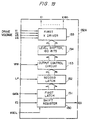
- FIG. 15 A block diagram of a drive circuit for scan signal electrodes (row electrodes), for implementing the drive methods of the first to the sixth embodiments, is shown in Fig. 15. The description below concerns the circuit that generates the drive waveform of the sixth embodiment.
- a logic circuit 110 generates a reset signal RE that specifies reset period T1 and a select signal S that specifies selection period T3 after delay period T2 has elapsed after reset period T1, based on information on delay period T2
- Signals RE and S are input to shift registers 111 and 112, respectively.
- Each of these registers 111 and 112 transfer signals RE and S in accordance with a shift clock SCK, and at the same time the internal states of the registers are simultaneously output in parallel to 160 channels.
- Y driver 115 receives three voltages from a power supply circuit 116 and a phase converter 117. If the power supply voltage of power supply circuit 116 acts as the alternation signal FR, each of the voltages can be made to swing ⁇ Va or ⁇ Vb.
- FIG. 16 A block diagram of the drive circuit for the data signal electrodes (column electrodes) is shown in Fig. 16.
- 8-bit image data D0 to D7 is input to a data latch circuit 121 through a multiplexer 120, and it is converted into 160 channels of parallel data in the data latch circuit 121.
- the latch timing of the data latch circuit 121 is determined by latch pulses output by a control circuit 122 to which the clock SCK is input.
- the 160 channels of image data are sent from data latch circuit 121 to a level shifter 123, and at the same time an inversion operation is added by a signal from a logic circuit 125, based on the alternation signal FR.
- An X driver 124 to which these four states for each of the channels are input selects one level from power supply voltages VL1 to VL4 in accordance with the state of each channel, and outputs it.
- VL1 V7
- VL2 V2
- VL3 V5
- VL V4
- a waveform that is the same as data signal Xm of Fig. 14, which shows the drive waveform of the sixth embodiment, can be generated.
- a liquid crystal panel 130 has a 320 x 320-pixel structure, and first and second Y driver circuits 131A and 131B and first and second X drivers 132A and 132B are provided in order to drive this liquid crystal panel 130.
- First and second Y driver circuits 131A and 131B each have the same configuration, which is shown in Fig. 18.
- X driver circuits 132A and 132B have the same configuration, which is shown in Fig. 19.
- Y driver circuit 131A has a shift register 140 that comprises a select shift register 140A and a reset shift register 140B.
- Select shift register 140A has registers SR1 to SR160 and reset shift register 140B has registers RR1 to RR160.
- Select signal S that specifies selection period T3, is input to select shift register 140A and is sequentially shifted by shift clock YSCL in the next-stage register.
- the contents of register SR160 are output from a select out pin, enabling a cascade connection with second Y driver circuit 131B.
- Reset signal RE which specifies reset period T1, is input to reset shift register 140B and is sequentially shifted by shift clock YSCL in the next-stage shift register.
- the contents of register RR160 are output through the reset out pin, enabling a cascade connection with second Y driver circuit 131B.
- All 160 channels of the contents of each of shift registers 140A and 140B are input to output control circuit 141.
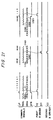
- V1Y, V2Y, V3Y, and V4Y are input to Y driver 143, and one drive voltage is output to each of the channels in accordance with the logical chart of Table 7, based on the six states identified and output by output control circuit 141.
- first and second Y driver circuits 131A and 131B are shown in Fig. 20.
- Fig. 20 if the length of selection period T3 is taken to be 1H, a signal YFR is repeatedly turned on and off every 1H and the polarity of the voltage applied to the liquid crystal inverts every 1H. Since each row has 320 pixels, the duty ratio is 1/320, and reset period T1 is set to 5H and delay period T2 to 2H.
- the signal waveform of the nth scan signal Yn output by the operation of this drive circuit is shown in Fig. 22.
- First X driver circuit 132A is described with reference to Fig. 19.
- First X driver circuit 132A has a shift register 150 that has 160 registers, and data is sequentially shifted in a next-stage register in accordance with an input signal EI and a shift clock XSCL.
- the contents of the 160th register are output to the outside through an EO pin, enabling a cascade connection with second X driver circuit 132B.
- Signal EI input to shift register 150 is at a logical one once every period 1 H, as shown in Fig. 21. Therefore, a logical one is output in sequence from each register of shift register 150, and this causes a first latch circuit 151 to latch image data at addresses corresponding to its registers.
- the 160 channels of data of first latch circuit 151 is latched in a second latch circuit 152 at the timing at which a latch pulse LP is input.
- X driver 155 receives four types of drive voltage V1X, V2X, V3X, and V4X, and outputs one of the four types of drive voltage to each channel in accordance with the logical chart of Table 8, based on information from output control circuit 153.
- This difference signal inverts the voltage applied to the liquid crystal every 1H, in the same manner as in the difference signal of Fig. 14 which shows the drive waveforms of the sixth embodiment. Since the voltage applied to the liquid crystal within one frame cannot be balanced between positive and negative, a balance between positive and negative in the voltage applied to the liquid crystal is achieved in the (k+1)th frame subsequent to the kth frame. This means that the difference signal shown in Fig. 22 combines a polarity inversion every 1H and a polarity inversion every frame, as in the sixth embodiment.
- the eighth embodiment is more advantageous than the seventh embodiment from a circuit configuration viewpoint, in that switching of the voltages of each of the scan and data signals is performed by logic means.
- a drive method that enables modification of delay period T2 within the signal, using the drive circuit shown for the eighth embodiment, is described with reference to Figs. 23-24.
- the means of changing delay period T2 must not only change the delay period without affecting the specified position of selection period T3 within one frame T, it must also change reset period T1 before delay period T2.
- reset period T1 is set to 5H and delay period T2 to 2H
- a combination reset plus delay signal having a pulse width that is the sum of the pulse widths of reset period T1 and delay period T2 (7H) is generated before selection period T3.
- the reset signal input to reset shift register 140B of Y driver circuits 131A and 131B can be shaped by an exclusive OR of this reset plus delay signal and the delay signal that specifies the delay period.
- delay period T2 if it becomes necessary to change delay period T2 to compensate for irregularities of the threshold value of the liquid crystal at individual pixels making up the liquid crystal panel, or for variations in the threshold value of the liquid crystal caused by ambient temperature, the specifications of delay period T2 and reset period T1 before it can be changed by the above means.
- a reset signal having the same 5H reset period T1 of Fig. 23 could be shaped by an exclusive OR of the thus modified delay signal and the reset plus delay signal.
- the method of the present invention to be described in the foregoing embodiments is suitable for driving a liquid crystal display device such as a TV, the display of a personal computer, a projector, a head mounted display, the viewfinder of a video camera, or a printer having a liquid crystal shutter.
- a liquid crystal display device such as a TV, the display of a personal computer, a projector, a head mounted display, the viewfinder of a video camera, or a printer having a liquid crystal shutter.
Abstract
Description
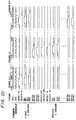
| Waveform | Duty Ratio | Pulse width T3/2(µs) | Delay Time (µs) | ON Voltage (V) | OFF Voltage (V) | ON/OFF Capability |
| Fig. 3 | 1/60 | 200 | 0 | 2 | 0 | |
| 1/120 | 100 | 0 | 2 | 0 | | |
| 1/240 | 50 | 0 | 3 | 0 | No |
| Waveform | Duty Ratio | Pulse Width (µs) | Delay Time (µs) | ON Voltage (V) | OFF Voltage (V) | ON/OFF Capability |
| Fig. | 1/240 | 100 (=T3) | 0 | 3 | 0 | No |
| 100 | 3 | 0 | | |||
| 200 | 3 | 0 | Yes | |||
| Fig. | 1/240 | 50 (=T3/2) | 0 | 3 | 0 | No |
| 50 | 3 | 0 | Yes | |||
| 100 | 3 | 0 | | |||
| 200 | 3 | 0 | Yes | |||
| Fig. | 1/480 | 50 (=T3) | 0 | 3 | 0 | No |
| 50 | 3 | 0 | No | |||
| 100 | 3 | 0 | No | |||
| 200 | 3 | 0 | | |||
| 0 | 5 | 0 | No | |||
| 50 | 5 | 0 | Yes | |||
| 100 | 5 | 0 | | |||
| 150 | 5 | 0 | Yes | |||
| Fig. | 1/480 | 25 (=T3/2) | 0 | 5 | 0 | No |
| 50 | 5 | 0 | Yes | |||
| 100 | 5 | 0 | Yes | |||
| 250 | 5 | 0 | Yes |
The drive waveform used to drive the simple matrix type of liquid crystal display panel of Fig. 5 is shown in Fig. 6. A
| Logical Values for Y Driver Output | |||
| Reset | Select | Y FR | Y OUT |
| L | L | L | V4Y |
| L | L | H | V3Y |
| L | H | L | V2Y |
| L | H | H | V1Y |
| H | L | L | V1Y |
| H | L | H | V2Y |
| H | H | * | * |
| (L: Low; H: High; *: Don't care) |
| Logical Values for Y Driver Output | ||
| Data | Y FR | X OUT |
| L | L | V2X |
| L | H | V1X |
| H | L | V4X |
| H | H | V3X |
| (L: Low; H: High) |
Claims (12)
- A method of driving a liquid crystal display device wherein said liquid crystal display device comprises:a chiral nematic liquid crystal medium wherein liquid crystal molecules interposed between two substrates have a predetermined angle of twist in an initial state and said chiral nematic liquid crystal medium has two metastable states differing from said initial state as relaxation states achieved after a voltage that brings about a Frederick's transition has been applied in said initial state;a plurality of row electrodes formed on one of said substrates, each being supplied with a row electrode signal; anda plurality of column electrodes formed on the other of said substrates, each being supplied with a column electrode signal;
wherein intersections between said row electrodes and said column electrodes form pixels and the voltage of a difference signal between said row electrode signal and said column electrode signal is applied to said liquid crystal corresponding to each of said pixels to drive said pixels;said method being characterized in using at least eight potential levels to drive said liquid crystal and comprising the steps of:a) including within one frame of said difference signal a selection period that is set to be shifted for each of said row electrodes, a nonselection period following thereafter, and a reset period set before said selection period;b) setting said column electrode signal to data potentials that include a potential that is either an ON potential or an OFF potential for each occurrence of said selection period corresponding to each of said pixels on the same column electrode, and setting four types of potential for applying positive and negative ON selection voltages and positive and negative OFF selection voltages to said liquid crystal, as said data potentials of said column electrode signal;c) setting said row electrode signal to a reset potential during said reset period, a selection potential during said selection period, and a nonselection potential during a nonselection period, said reset potential being two types of potential for applying positive and negative reset voltages to said liquid crystal during said reset period, said selection potential being two types of potential for applying positive and negative selection voltages to said liquid crystal during said selection period, and said nonselection potential being two types of potential for imposing a bias potential on said four types of data potential during said nonselection period; andd) setting either two types of said selection potential or two potentials among said four types of said data potential to be the same as said two types of said reset potential. - The method of Claim 1, including the steps of:dividing said eight potential levels into two groups such that four levels are in a first, low-voltage group (V1, V2, V3, and V4, where: V1 < V2 < V3 < V4) and four levels are in a second, high-voltage group (V5, V6, V7, and V8, where: V4 < V5 < V6 < V7 < V8);selecting said reset potential from amongst said second group when said data potential of said column electrode signal lies within said first group, or from amongst said first group when said data potential of said column electrode signal lies within said second group; andin said periods other than said reset period, selecting one potential each from the same first group when said data potential of said column electrode signal is within said first group, or selecting one potential each from the same second group when said data potential of said column electrode signal is within said second group.
- The method of Claim 2, including the step of:setting the potential difference between said potential V4 of said first group and said potential VS of said second group to be large, and setting the absolute value of said reset voltage applied to said liquid crystal in said reset period to be large.
- The method of Claim 2 or 3, including the steps of:in a kth frame (where k is an integer), setting an ON selection potential of said column electrode signal to V5 of said second group and an OFF selection potential to V7; and setting said reset potential of said row electrode signal to V1, said selection potential to V8, and said nonselection potential to V6; andin a subsequent (k+1)th frame, setting said ON selection potential of said column electrode signal to V4 of said first group and said OFF selection potential to V2; and setting said reset potential of said row electrode signal to V8, said selection potential to V1, and said nonselection potential to V3; whereby said liquid crystal is driven in an alternating manner by a polarity inversion every frame.
- The method of Claim 2 or 3, including the steps of:in a kth frame (where k is an integer), setting an ON selection potential of said column electrode signal to V8 of said second group and an OFF selection potential to V6; and setting said reset potential of said row electrode signal to V1, said selection potential to V5, and said nonselection potential to V7; andin a subsequent (k+1)th frame, setting said ON selection potential of said column electrode signal to V1 of said first group and said OFF selection potential to V3; and setting said reset potential of said row electrode signal to V8, said selection potential to V4, and said nonselection potential to V2; whereby said liquid crystal is driven in an alternating manner by a polarity inversion every frame.
- The method of Claim 2 or 3 further comprising the steps of:setting, within the period of one frame, an ON selection potential of said column electrode signal by alternating pulses of V4 and V5;setting, within the period of one frame, an OFF selection potential of said column electrode signal by alternating pulses of V2 and V7; andin a sequence corresponding thereto, said reset potential of said row electrode signal is set by alternating pulses of V8 and V1, said selection potential is set by alternating pulses of V1 and V8, and said nonselection potential is set by alternating pulses of V3 and V6, whereby the polarity of each voltage applied to said liquid crystal is inverted at each pulse.
- The method of Claim 4 or 6 wherein:said voltages are set to be in the relationship: V4 - V3 = V3 - V2 = V7 - V6 = V6 - V5.
- The method of Claim 2 or 3 further comprising the steps of:setting, within the period of one frame, an ON selection potential of said column electrode signal by alternating pulses of V1 and V8;setting, within the period of one frame, an OFF selection potential of said column electrode signal by alternating pulses of V3 and V6; andin a sequence corresponding thereto, said reset potential of said row electrode signal is set by alternating pulses of V8 and V1, said selection potential is set by alternating pulses of V4 and V5, and said nonselection potential is set by alternating pulses of V2 and V7, whereby the polarity of each voltage applied to said liquid crystal is inverted at each pulse.
- The method of Claim 5 or 8 wherein said voltages are set to be in the relationship: V3 - V2 = V2 - V1 = V8 - V7 = V7 - V6.
- The method of Claim 6 or 8 wherein when a unit time equivalent to said selection period is termed 1H, the pulse width of a signal FR that causes said row electrode signal and column electrode signal to alternate is 1H, and the phase of said signal FR is set to be shifted by (1H/2) with respect to the selection period of said row electrode signal Yn.
- The method of Claim 6 or 8, including the step of:driving said liquid crystal in an alternating manner by a combination of a polarity inversion every unit time (1H) equivalent to said selection period and a polarity inversion every frame, such that the polarity of a voltage applied to said liquid crystal is inverted every 1 H, and, when said polarity at the start of a kth frame (where k is an integer) is positive the polarity at the start of the (k+1)th frame is made negative, when said polarity at the start of a kth frame (where k is an integer) is negative the polarity at the start of the (k+1)th frame is made positive.
- The method of any one of Claims 2 to 11, including the step of:setting said first group of voltages and second group of voltages to be symmetrical in the positive and negative directions with respect to a center of the ground-level potential.
Applications Claiming Priority (19)
| Application Number | Priority Date | Filing Date | Title |
|---|---|---|---|
| JP37057/93 | 1993-02-25 | ||
| JP3705793 | 1993-02-25 | ||
| JP3705793 | 1993-02-25 | ||
| JP12170693 | 1993-05-24 | ||
| JP121706/93 | 1993-05-24 | ||
| JP12170693 | 1993-05-24 | ||
| JP19860493 | 1993-08-10 | ||
| JP19860493 | 1993-08-10 | ||
| JP198604/93 | 1993-08-10 | ||
| JP26389893 | 1993-10-21 | ||
| JP26389893 | 1993-10-21 | ||
| JP263898/93 | 1993-10-21 | ||
| JP27573693 | 1993-11-04 | ||
| JP27573693 | 1993-11-04 | ||
| JP275736/93 | 1993-11-04 | ||
| JP352493/93 | 1993-12-29 | ||
| JP35249393A JP3489169B2 (en) | 1993-02-25 | 1993-12-29 | Driving method of liquid crystal display device |
| JP35249393 | 1993-12-29 | ||
| EP94102831A EP0613116B1 (en) | 1993-02-25 | 1994-02-24 | Method of driving a liquid crystal display device |
Related Parent Applications (1)
| Application Number | Title | Priority Date | Filing Date |
|---|---|---|---|
| EP94102831A Division EP0613116B1 (en) | 1993-02-25 | 1994-02-24 | Method of driving a liquid crystal display device |
Publications (2)
| Publication Number | Publication Date |
|---|---|
| EP0866441A1 true EP0866441A1 (en) | 1998-09-23 |
| EP0866441B1 EP0866441B1 (en) | 2001-09-26 |
Family
ID=27549841
Family Applications (2)
| Application Number | Title | Priority Date | Filing Date |
|---|---|---|---|
| EP98110226A Expired - Lifetime EP0866441B1 (en) | 1993-02-25 | 1994-02-24 | Method of driving a liquid crystal display device using 8 voltage levels |
| EP94102831A Expired - Lifetime EP0613116B1 (en) | 1993-02-25 | 1994-02-24 | Method of driving a liquid crystal display device |
Family Applications After (1)
| Application Number | Title | Priority Date | Filing Date |
|---|---|---|---|
| EP94102831A Expired - Lifetime EP0613116B1 (en) | 1993-02-25 | 1994-02-24 | Method of driving a liquid crystal display device |
Country Status (7)
| Country | Link |
|---|---|
| US (3) | US5684503A (en) |
| EP (2) | EP0866441B1 (en) |
| JP (1) | JP3489169B2 (en) |
| KR (1) | KR100238903B1 (en) |
| DE (2) | DE69424330T2 (en) |
| HK (1) | HK1014288A1 (en) |
| SG (1) | SG72608A1 (en) |
Families Citing this family (113)
| Publication number | Priority date | Publication date | Assignee | Title |
|---|---|---|---|---|
| IT1271866B (en) * | 1994-02-25 | 1997-06-09 | Univ Roma | METHOD OF CONTROL OF A FERROELECTRIC LIQUID CRYSTAL MATERIAL PANEL. |
| US6154190A (en) * | 1995-02-17 | 2000-11-28 | Kent State University | Dynamic drive methods and apparatus for a bistable liquid crystal display |
| JP3603904B2 (en) * | 1995-04-25 | 2004-12-22 | シチズン時計株式会社 | Driving method and apparatus for antiferroelectric liquid crystal display element |
| KR100254647B1 (en) | 1995-05-17 | 2000-05-01 | 야스카와 히데아키 | Liquid crystal display device and its drive method and the drive circuit and power supply circuit used therein |
| US5945971A (en) * | 1995-07-03 | 1999-08-31 | Citizen Watch Co., Ltd. | Liquid crystal display device |
| US7999787B2 (en) | 1995-07-20 | 2011-08-16 | E Ink Corporation | Methods for driving electrophoretic displays using dielectrophoretic forces |
| US7193625B2 (en) | 1999-04-30 | 2007-03-20 | E Ink Corporation | Methods for driving electro-optic displays, and apparatus for use therein |
| JPH09171170A (en) * | 1995-12-20 | 1997-06-30 | Denso Corp | Matrix type liquid crystal display device |
| JP3442581B2 (en) * | 1996-08-06 | 2003-09-02 | 株式会社ヒューネット | Driving method of nematic liquid crystal |
| WO1998008132A1 (en) | 1996-08-19 | 1998-02-26 | Seiko Epson Corporation | Method of driving liquid crystal device |
| JP3529999B2 (en) * | 1997-02-06 | 2004-05-24 | 株式会社リコー | Liquid crystal cell and driving method thereof |
| JP3342341B2 (en) * | 1997-03-13 | 2002-11-05 | キヤノン株式会社 | Liquid crystal device and driving method of liquid crystal device |
| GB9717597D0 (en) * | 1997-08-21 | 1997-10-22 | Sharp Kk | Liquid crystal device |
| JPH1164823A (en) | 1997-08-21 | 1999-03-05 | Denso Corp | Matrix type liquid crystal display device |
| US20010052885A1 (en) * | 1997-09-12 | 2001-12-20 | Masaya Okita | Method for driving a nematic liquid crystal |
| JP3659013B2 (en) | 1997-10-22 | 2005-06-15 | セイコーエプソン株式会社 | Liquid crystal device, driving method thereof and electronic apparatus using the same |
| CN1516102A (en) * | 1998-02-09 | 2004-07-28 | 精工爱普生株式会社 | Liquid crystal display device and driving method, and electronic device using said liquid crystal display |
| JPH11296150A (en) | 1998-04-10 | 1999-10-29 | Masaya Okita | High-speed driving method for liquid crystal |
| WO2000008626A1 (en) * | 1998-08-03 | 2000-02-17 | Seiko Epson Corporation | Electrooptic device, substrate therefor, electronic device, and projection display |
| US6323834B1 (en) * | 1998-10-08 | 2001-11-27 | International Business Machines Corporation | Micromechanical displays and fabrication method |
| JP2000310969A (en) * | 1999-02-25 | 2000-11-07 | Canon Inc | Picture display device and its driving method |
| JP2000267070A (en) * | 1999-03-18 | 2000-09-29 | Alps Electric Co Ltd | Liquid crystal display device and its driving method |
| US7119772B2 (en) * | 1999-04-30 | 2006-10-10 | E Ink Corporation | Methods for driving bistable electro-optic displays, and apparatus for use therein |
| US7012600B2 (en) | 1999-04-30 | 2006-03-14 | E Ink Corporation | Methods for driving bistable electro-optic displays, and apparatus for use therein |
| US6507330B1 (en) * | 1999-09-01 | 2003-01-14 | Displaytech, Inc. | DC-balanced and non-DC-balanced drive schemes for liquid crystal devices |
| KR100641729B1 (en) * | 1999-09-22 | 2006-11-02 | 엘지.필립스 엘시디 주식회사 | Reset Method of Liquid Crystal Display and Apparatus Thereof |
| JP3618066B2 (en) * | 1999-10-25 | 2005-02-09 | 株式会社日立製作所 | Liquid crystal display |
| JP3606138B2 (en) * | 1999-11-05 | 2005-01-05 | セイコーエプソン株式会社 | Driver IC, electro-optical device and electronic apparatus |
| JP2001215932A (en) * | 1999-11-22 | 2001-08-10 | Sharp Corp | Display device and its driving method |
| KR100734927B1 (en) * | 1999-12-27 | 2007-07-03 | 엘지.필립스 엘시디 주식회사 | Lcd |
| US6717561B1 (en) * | 2000-01-31 | 2004-04-06 | Three-Five Systems, Inc. | Driving a liquid crystal display |
| US6812913B2 (en) * | 2000-02-17 | 2004-11-02 | Minolta Co., Ltd. | Liquid crystal display driving method and liquid crystal display device |
| JP3486599B2 (en) * | 2000-03-31 | 2004-01-13 | キヤノン株式会社 | Driving method of liquid crystal element |
| KR20020032439A (en) * | 2000-04-25 | 2002-05-03 | 요트.게.아. 롤페즈 | Driving of display device for obtaining gray scales |
| GB0010825D0 (en) * | 2000-05-04 | 2000-06-28 | Varintelligent Bvi Ltd | Matrix driving schemes for cholesteric liquid crystal displays |
| JP4706123B2 (en) * | 2000-05-29 | 2011-06-22 | コニカミノルタホールディングス株式会社 | Liquid crystal display device and method for driving liquid crystal display element |
| GB2367177A (en) * | 2000-09-23 | 2002-03-27 | Sharp Kk | Operating a bistable liquid crystal display |
| JP4166448B2 (en) * | 2000-10-06 | 2008-10-15 | シャープ株式会社 | Active matrix liquid crystal display device and driving method thereof |
| US7023409B2 (en) | 2001-02-09 | 2006-04-04 | Kent Displays, Incorporated | Drive schemes for gray scale bistable cholesteric reflective displays utilizing variable frequency pulses |
| JP4258128B2 (en) * | 2001-03-13 | 2009-04-30 | コニカミノルタホールディングス株式会社 | Method for driving liquid crystal display element and liquid crystal display device |
| TW574512B (en) * | 2001-03-14 | 2004-02-01 | Koninkl Philips Electronics Nv | Electrophoretic display device |
| JP3804502B2 (en) * | 2001-09-27 | 2006-08-02 | カシオ計算機株式会社 | Driving method of liquid crystal display device |
| JP2003134520A (en) * | 2001-10-19 | 2003-05-09 | Minolta Co Ltd | Digital camera |
| CN102789758B (en) * | 2001-11-20 | 2016-05-18 | 伊英克公司 | Drive the method for bistable electro-optic displays |
| US8125501B2 (en) | 2001-11-20 | 2012-02-28 | E Ink Corporation | Voltage modulated driver circuits for electro-optic displays |
| US8593396B2 (en) | 2001-11-20 | 2013-11-26 | E Ink Corporation | Methods and apparatus for driving electro-optic displays |
| US9412314B2 (en) | 2001-11-20 | 2016-08-09 | E Ink Corporation | Methods for driving electro-optic displays |
| US9530363B2 (en) | 2001-11-20 | 2016-12-27 | E Ink Corporation | Methods and apparatus for driving electro-optic displays |
| US8558783B2 (en) | 2001-11-20 | 2013-10-15 | E Ink Corporation | Electro-optic displays with reduced remnant voltage |
| US7952557B2 (en) * | 2001-11-20 | 2011-05-31 | E Ink Corporation | Methods and apparatus for driving electro-optic displays |
| US7528822B2 (en) * | 2001-11-20 | 2009-05-05 | E Ink Corporation | Methods for driving electro-optic displays |
| JP3928438B2 (en) * | 2001-11-30 | 2007-06-13 | コニカミノルタホールディングス株式会社 | Method for driving liquid crystal display element, driving device and liquid crystal display device |
| US7126577B2 (en) | 2002-03-15 | 2006-10-24 | Koninklijke Philips Electronics N.V. | Electrophoretic active matrix display device |
| JP3637911B2 (en) | 2002-04-24 | 2005-04-13 | セイコーエプソン株式会社 | Electronic device, electronic apparatus, and driving method of electronic device |
| JP4486319B2 (en) * | 2002-05-09 | 2010-06-23 | 三星電子株式会社 | Gradation voltage generator, gradation voltage generation method, and reflection-transmission type liquid crystal display device using the same |
| KR20050004203A (en) * | 2002-05-24 | 2005-01-12 | 코닌클리케 필립스 일렉트로닉스 엔.브이. | An electrophoretic display and a method of driving an electrophoretic display |
| US20080024482A1 (en) | 2002-06-13 | 2008-01-31 | E Ink Corporation | Methods for driving electro-optic displays |
| US20110199671A1 (en) * | 2002-06-13 | 2011-08-18 | E Ink Corporation | Methods for driving electrophoretic displays using dielectrophoretic forces |
| JP2004029477A (en) * | 2002-06-26 | 2004-01-29 | Fujitsu Ltd | Driving method of liquid crystal display, and liquid crystal display |
| TW586105B (en) * | 2002-07-09 | 2004-05-01 | Au Optronics Corp | Continuous pulse array generator using low-voltage clock signal |
| TW580681B (en) * | 2002-08-13 | 2004-03-21 | Toppoly Optoelectronics Corp | Power-saving liquid crystal display and power-saving operation method |
| JP3887285B2 (en) * | 2002-08-27 | 2007-02-28 | ローム株式会社 | Display device |
| JP3812558B2 (en) * | 2002-09-20 | 2006-08-23 | セイコーエプソン株式会社 | Liquid crystal device, driving method thereof, and electronic apparatus |
| GB0223556D0 (en) * | 2002-10-10 | 2002-11-20 | Central Research Lab Ltd | Driving DAP liquid crystal devices |
| US20130063333A1 (en) | 2002-10-16 | 2013-03-14 | E Ink Corporation | Electrophoretic displays |
| JP4136670B2 (en) * | 2003-01-09 | 2008-08-20 | キヤノン株式会社 | Matrix panel drive control apparatus and drive control method |
| KR20050092779A (en) | 2003-01-23 | 2005-09-22 | 코닌클리케 필립스 일렉트로닉스 엔.브이. | Driving a bi-stable matrix display device |
| AU2003233105A1 (en) * | 2003-01-23 | 2004-08-13 | Koninklijke Philips Electronics N.V. | Electrophoretic display device and driving method therefor |
| JP2006516747A (en) * | 2003-01-23 | 2006-07-06 | コーニンクレッカ フィリップス エレクトロニクス エヌ ヴィ | Driving bistable matrix display devices |
| JP2006526162A (en) * | 2003-01-23 | 2006-11-16 | コーニンクレッカ フィリップス エレクトロニクス エヌ ヴィ | Driving an electrophoretic display |
| US10726798B2 (en) | 2003-03-31 | 2020-07-28 | E Ink Corporation | Methods for operating electro-optic displays |
| WO2004104979A2 (en) * | 2003-05-16 | 2004-12-02 | Sipix Imaging, Inc. | Improved passive matrix electrophoretic display driving scheme |
| US8174490B2 (en) | 2003-06-30 | 2012-05-08 | E Ink Corporation | Methods for driving electrophoretic displays |
| EP2698784B1 (en) | 2003-08-19 | 2017-11-01 | E Ink Corporation | Electro-optic display |
| CN100557676C (en) * | 2003-09-12 | 2009-11-04 | 皇家飞利浦电子股份有限公司 | The temperature dependent method of compensation driving schemes for electrophoretic displays |
| JP4948170B2 (en) * | 2003-09-12 | 2012-06-06 | アドレア エルエルシー | Method for compensating temperature dependence of driving scheme for electrophoretic display |
| CN1853216A (en) * | 2003-09-18 | 2006-10-25 | 皇家飞利浦电子股份有限公司 | An electrophoretic display with reduced look-up-table memory |
| WO2005027086A1 (en) * | 2003-09-18 | 2005-03-24 | Koninklijke Philips Electronics N.V. | Temperature compensation method for bi-stable display using drive sub-pulses |
| WO2005029458A1 (en) * | 2003-09-19 | 2005-03-31 | E Ink Corporation | Methods for reducing edge effects in electro-optic displays |
| US7633470B2 (en) * | 2003-09-29 | 2009-12-15 | Michael Gillis Kane | Driver circuit, as for an OLED display |
| US8928562B2 (en) * | 2003-11-25 | 2015-01-06 | E Ink Corporation | Electro-optic displays, and methods for driving same |
| KR101026809B1 (en) * | 2003-12-19 | 2011-04-04 | 삼성전자주식회사 | Impulsive driving liquid crystal display and driving method thereof |
| CN100458906C (en) | 2004-02-20 | 2009-02-04 | 三星电子株式会社 | Pulse compensator, display device and method of driving the display device |
| US7492339B2 (en) * | 2004-03-26 | 2009-02-17 | E Ink Corporation | Methods for driving bistable electro-optic displays |
| KR101021444B1 (en) * | 2004-04-16 | 2011-03-15 | 엘지디스플레이 주식회사 | Field Sequential color LCD and driving method thereof |
| US11250794B2 (en) | 2004-07-27 | 2022-02-15 | E Ink Corporation | Methods for driving electrophoretic displays using dielectrophoretic forces |
| US7453445B2 (en) | 2004-08-13 | 2008-11-18 | E Ink Corproation | Methods for driving electro-optic displays |
| US7948464B2 (en) * | 2004-09-29 | 2011-05-24 | Citizen Holdings Co., Ltd. | Memory-type liquid crystal display device |
| KR100685817B1 (en) * | 2005-02-18 | 2007-02-22 | 삼성에스디아이 주식회사 | Field Sequential Liquid Crystal Display |
| KR100685816B1 (en) * | 2005-02-18 | 2007-02-22 | 삼성에스디아이 주식회사 | Method of Field Sequential Operation and Field Sequential Liquid Crystal Display |
| KR100685819B1 (en) * | 2005-02-18 | 2007-02-22 | 삼성에스디아이 주식회사 | Field Sequential Liquid Crystal Display of performing Initialization Operation |
| JP2007094008A (en) * | 2005-09-29 | 2007-04-12 | Hitachi Displays Ltd | Display device |
| CN101310320B (en) * | 2005-11-15 | 2011-02-16 | 皇家飞利浦电子股份有限公司 | Driving means for electrowetting displays |
| US8106674B2 (en) * | 2006-10-31 | 2012-01-31 | Lc Vision, Llc | Automated liquid crystal analysis instrument |
| KR101384283B1 (en) * | 2006-11-20 | 2014-04-11 | 삼성디스플레이 주식회사 | Liquid crystal display and driving method thereof |
| WO2008075419A1 (en) * | 2006-12-20 | 2008-06-26 | Fujitsu Limited | Liquid crystal display element and electronic paper using the same |
| EP2124098A4 (en) * | 2007-02-21 | 2011-07-27 | Konica Minolta Holdings Inc | Display element driving method |
| JP2008242379A (en) * | 2007-03-29 | 2008-10-09 | Seiko Epson Corp | Display drive device, display device, and electronic apparatus |
| US8068079B2 (en) * | 2007-10-18 | 2011-11-29 | Canon Kabushiki Kaisha | Liquid crystal display apparatus |
| US8933869B2 (en) * | 2008-03-27 | 2015-01-13 | Citizen Holdings Co., Ltd. | Ferroelectric liquid crystal panel driving method and liquid crystal display device |
| TW201039307A (en) * | 2009-04-24 | 2010-11-01 | Princeton Technology Corp | Liquid crystal display |
| JP5437737B2 (en) * | 2009-08-19 | 2014-03-12 | セイコーインスツル株式会社 | Bistable liquid crystal display panel and driving method thereof |
| US8217930B2 (en) * | 2009-08-27 | 2012-07-10 | 3M Innovative Properties Company | Fast transitions of large area cholesteric displays |
| JP5293532B2 (en) * | 2009-09-24 | 2013-09-18 | セイコーエプソン株式会社 | Integrated circuit device and electronic apparatus |
| TWI591604B (en) | 2010-04-09 | 2017-07-11 | 電子墨水股份有限公司 | Methods for driving electro-optic displays |
| JP5341826B2 (en) * | 2010-06-18 | 2013-11-13 | セイコーインスツル株式会社 | Method and device for driving bistable liquid crystal display panel |
| TWI415051B (en) * | 2010-09-15 | 2013-11-11 | Au Optronics Corp | Lcd driving circuit and related driving method |
| KR101773950B1 (en) * | 2010-11-08 | 2017-09-13 | 삼성디스플레이 주식회사 | Display device and driving method thereof |
| EP3061083B1 (en) * | 2013-10-21 | 2022-04-20 | NXP USA, Inc. | A control unit for a segment liquid crystal display and a method thereof |
| TWI524324B (en) * | 2014-01-28 | 2016-03-01 | 友達光電股份有限公司 | Liquid crystal display |
| KR102460546B1 (en) * | 2016-09-30 | 2022-10-31 | 엘지디스플레이 주식회사 | Organic light emitting display device and controlling method thereof |
| JP2022545991A (en) * | 2020-07-30 | 2022-11-02 | 深▲せん▼市艾比森光電股▲ふん▼有限公司 | LED display correction method and related device |
| CN111951696B (en) * | 2020-07-30 | 2022-10-25 | 深圳市艾比森光电股份有限公司 | Correction method and related device for LED display screen |
Citations (3)
| Publication number | Priority date | Publication date | Assignee | Title |
|---|---|---|---|---|
| EP0300755A2 (en) * | 1987-07-21 | 1989-01-25 | THORN EMI plc | Drive circuit |
| US4850676A (en) * | 1985-07-31 | 1989-07-25 | Seiko Epson Corporation | Method for driving a liquid crystal element |
| EP0379326A1 (en) * | 1989-01-17 | 1990-07-25 | Fujitsu Limited | Liquid crystal material and display device using same |
Family Cites Families (8)
| Publication number | Priority date | Publication date | Assignee | Title |
|---|---|---|---|---|
| US4701026A (en) * | 1984-06-11 | 1987-10-20 | Seiko Epson Kabushiki Kaisha | Method and circuits for driving a liquid crystal display device |
| GB2173337B (en) * | 1985-04-03 | 1989-01-11 | Stc Plc | Addressing liquid crystal cells |
| US4952032A (en) * | 1987-03-31 | 1990-08-28 | Canon Kabushiki Kaisha | Display device |
| GB2249653B (en) * | 1990-10-01 | 1994-09-07 | Marconi Gec Ltd | Ferroelectric liquid crystal devices |
| DE69220173T2 (en) * | 1991-10-07 | 1997-09-18 | Fujitsu Ltd | Method for controlling a surface stabilized ferroelectric liquid crystal display element to increase the gray level number |
| SG63551A1 (en) * | 1992-05-07 | 1999-03-30 | Seiko Epson Corp | Liquid crystal display device having two metastable states and its driving method |
| JP3753440B2 (en) * | 1992-05-07 | 2006-03-08 | セイコーエプソン株式会社 | Liquid crystal display device and driving method of liquid crystal display device |
| JP3634390B2 (en) * | 1992-07-16 | 2005-03-30 | セイコーエプソン株式会社 | Liquid crystal electro-optic element |
-
1993
- 1993-12-29 JP JP35249393A patent/JP3489169B2/en not_active Expired - Fee Related
-
1994
- 1994-02-18 US US08/199,369 patent/US5684503A/en not_active Expired - Lifetime
- 1994-02-24 EP EP98110226A patent/EP0866441B1/en not_active Expired - Lifetime
- 1994-02-24 DE DE69424330T patent/DE69424330T2/en not_active Expired - Lifetime
- 1994-02-24 DE DE69428465T patent/DE69428465T2/en not_active Expired - Fee Related
- 1994-02-24 SG SG1996001227A patent/SG72608A1/en unknown
- 1994-02-24 EP EP94102831A patent/EP0613116B1/en not_active Expired - Lifetime
- 1994-02-25 KR KR1019940003696A patent/KR100238903B1/en active IP Right Grant
-
1997
- 1997-04-18 US US08/837,506 patent/US5835075A/en not_active Expired - Fee Related
-
1998
- 1998-10-29 US US09/183,602 patent/US6236385B1/en not_active Expired - Fee Related
- 1998-12-24 HK HK98115542A patent/HK1014288A1/en not_active IP Right Cessation
Patent Citations (3)
| Publication number | Priority date | Publication date | Assignee | Title |
|---|---|---|---|---|
| US4850676A (en) * | 1985-07-31 | 1989-07-25 | Seiko Epson Corporation | Method for driving a liquid crystal element |
| EP0300755A2 (en) * | 1987-07-21 | 1989-01-25 | THORN EMI plc | Drive circuit |
| EP0379326A1 (en) * | 1989-01-17 | 1990-07-25 | Fujitsu Limited | Liquid crystal material and display device using same |
Also Published As
| Publication number | Publication date |
|---|---|
| EP0866441B1 (en) | 2001-09-26 |
| JPH07175041A (en) | 1995-07-14 |
| EP0613116A3 (en) | 1995-09-13 |
| DE69424330D1 (en) | 2000-06-15 |
| EP0613116B1 (en) | 2000-05-10 |
| JP3489169B2 (en) | 2004-01-19 |
| US5835075A (en) | 1998-11-10 |
| KR940020154A (en) | 1994-09-15 |
| KR100238903B1 (en) | 2000-01-15 |
| EP0613116A2 (en) | 1994-08-31 |
| DE69428465D1 (en) | 2001-10-31 |
| US6236385B1 (en) | 2001-05-22 |
| DE69428465T2 (en) | 2002-04-25 |
| HK1014288A1 (en) | 1999-09-24 |
| US5684503A (en) | 1997-11-04 |
| DE69424330T2 (en) | 2000-11-09 |
| SG72608A1 (en) | 2000-05-23 |
Similar Documents
| Publication | Publication Date | Title |
|---|---|---|
| EP0866441B1 (en) | Method of driving a liquid crystal display device using 8 voltage levels | |
| KR100627762B1 (en) | Flat display panel driving method and flat display device | |
| US6154191A (en) | System and method for driving a nematic liquid crystal | |
| US5488388A (en) | Liquid crystal apparatus | |
| JPH01134346A (en) | Ferrodielectric liquid crystal display device, driving thereof and generation of drive waveform | |
| JP2006524365A (en) | Display system with frame buffer and power saving sequence | |
| JP4879379B2 (en) | Driving method of liquid crystal display device | |
| JP3891018B2 (en) | Method for driving liquid crystal display element, driving device and liquid crystal display device | |
| JPH0954299A (en) | Liquid crystal display device | |
| US6307533B1 (en) | Liquid crystal display device with matrix electrode structure | |
| JP2003202540A (en) | Liquid crystal optical device | |
| JP3555578B2 (en) | Driving method of liquid crystal display device | |
| JP3525895B2 (en) | Driving method of liquid crystal display device | |
| JP2578490B2 (en) | Driving method of display device | |
| JP2637517B2 (en) | Liquid crystal device | |
| JPH08297302A (en) | Method for driving liquid crystal display device | |
| JPH11212062A (en) | Antiferroelectric liquid crystal display device and driving method therefor | |
| JP2001228462A (en) | Driving method for liquid crystal display device | |
| JPH02113219A (en) | Liquid crystal device | |
| JPH1124043A (en) | Liquid crystal display device and its driving method | |
| JPH09265078A (en) | Liquid crystal picture display device and multiplexing driving method | |
| JPS63249130A (en) | Liquid crystal device | |
| JPH07128641A (en) | Liquid crystal display device | |
| JPH02116822A (en) | Liquid crystal device | |
| JPH08184812A (en) | Anti-ferroelectric liquid crystal display driving method |
Legal Events
| Date | Code | Title | Description |
|---|---|---|---|
| PUAI | Public reference made under article 153(3) epc to a published international application that has entered the european phase |
Free format text: ORIGINAL CODE: 0009012 |
|
| AC | Divisional application: reference to earlier application |
Ref document number: 613116 Country of ref document: EP |
|
| AK | Designated contracting states |
Kind code of ref document: A1 Designated state(s): DE FR GB |
|
| 17P | Request for examination filed |
Effective date: 19981008 |
|
| GRAG | Despatch of communication of intention to grant |
Free format text: ORIGINAL CODE: EPIDOS AGRA |
|
| 17Q | First examination report despatched |
Effective date: 19991011 |
|
| GRAG | Despatch of communication of intention to grant |
Free format text: ORIGINAL CODE: EPIDOS AGRA |
|
| GRAG | Despatch of communication of intention to grant |
Free format text: ORIGINAL CODE: EPIDOS AGRA |
|
| GRAH | Despatch of communication of intention to grant a patent |
Free format text: ORIGINAL CODE: EPIDOS IGRA |
|
| GRAH | Despatch of communication of intention to grant a patent |
Free format text: ORIGINAL CODE: EPIDOS IGRA |
|
| GRAA | (expected) grant |
Free format text: ORIGINAL CODE: 0009210 |
|
| AC | Divisional application: reference to earlier application |
Ref document number: 613116 Country of ref document: EP |
|
| AK | Designated contracting states |
Kind code of ref document: B1 Designated state(s): DE FR GB |
|
| REF | Corresponds to: |
Ref document number: 69428465 Country of ref document: DE Date of ref document: 20011031 |
|
| REG | Reference to a national code |
Ref country code: GB Ref legal event code: IF02 |
|
| ET | Fr: translation filed | ||
| PLBE | No opposition filed within time limit |
Free format text: ORIGINAL CODE: 0009261 |
|
| STAA | Information on the status of an ep patent application or granted ep patent |
Free format text: STATUS: NO OPPOSITION FILED WITHIN TIME LIMIT |
|
| 26N | No opposition filed | ||
| PGFP | Annual fee paid to national office [announced via postgrant information from national office to epo] |
Ref country code: GB Payment date: 20070221 Year of fee payment: 14 |
|
| PGFP | Annual fee paid to national office [announced via postgrant information from national office to epo] |
Ref country code: DE Payment date: 20070222 Year of fee payment: 14 |
|
| PGFP | Annual fee paid to national office [announced via postgrant information from national office to epo] |
Ref country code: FR Payment date: 20070208 Year of fee payment: 14 |
|
| GBPC | Gb: european patent ceased through non-payment of renewal fee |
Effective date: 20080224 |
|
| REG | Reference to a national code |
Ref country code: FR Ref legal event code: ST Effective date: 20081031 |
|
| PG25 | Lapsed in a contracting state [announced via postgrant information from national office to epo] |
Ref country code: DE Free format text: LAPSE BECAUSE OF NON-PAYMENT OF DUE FEES Effective date: 20080902 |
|
| PG25 | Lapsed in a contracting state [announced via postgrant information from national office to epo] |
Ref country code: FR Free format text: LAPSE BECAUSE OF NON-PAYMENT OF DUE FEES Effective date: 20080229 |
|
| PG25 | Lapsed in a contracting state [announced via postgrant information from national office to epo] |
Ref country code: GB Free format text: LAPSE BECAUSE OF NON-PAYMENT OF DUE FEES Effective date: 20080224 |