JP3887285B2 - Display device - Google Patents
Display device Download PDFInfo
- Publication number
- JP3887285B2 JP3887285B2 JP2002246325A JP2002246325A JP3887285B2 JP 3887285 B2 JP3887285 B2 JP 3887285B2 JP 2002246325 A JP2002246325 A JP 2002246325A JP 2002246325 A JP2002246325 A JP 2002246325A JP 3887285 B2 JP3887285 B2 JP 3887285B2
- Authority
- JP
- Japan
- Prior art keywords
- temperature
- temperature sensor
- display device
- booster circuit
- voltage
- Prior art date
- Legal status (The legal status is an assumption and is not a legal conclusion. Google has not performed a legal analysis and makes no representation as to the accuracy of the status listed.)
- Expired - Fee Related
Links
Images


Classifications
-
- H—ELECTRICITY
- H02—GENERATION; CONVERSION OR DISTRIBUTION OF ELECTRIC POWER
- H02M—APPARATUS FOR CONVERSION BETWEEN AC AND AC, BETWEEN AC AND DC, OR BETWEEN DC AND DC, AND FOR USE WITH MAINS OR SIMILAR POWER SUPPLY SYSTEMS; CONVERSION OF DC OR AC INPUT POWER INTO SURGE OUTPUT POWER; CONTROL OR REGULATION THEREOF
- H02M3/00—Conversion of dc power input into dc power output
- H02M3/02—Conversion of dc power input into dc power output without intermediate conversion into ac
- H02M3/04—Conversion of dc power input into dc power output without intermediate conversion into ac by static converters
- H02M3/06—Conversion of dc power input into dc power output without intermediate conversion into ac by static converters using resistors or capacitors, e.g. potential divider
- H02M3/07—Conversion of dc power input into dc power output without intermediate conversion into ac by static converters using resistors or capacitors, e.g. potential divider using capacitors charged and discharged alternately by semiconductor devices with control electrode, e.g. charge pumps
- H02M3/073—Charge pumps of the Schenkel-type
-
- G—PHYSICS
- G09—EDUCATION; CRYPTOGRAPHY; DISPLAY; ADVERTISING; SEALS
- G09G—ARRANGEMENTS OR CIRCUITS FOR CONTROL OF INDICATING DEVICES USING STATIC MEANS TO PRESENT VARIABLE INFORMATION
- G09G3/00—Control arrangements or circuits, of interest only in connection with visual indicators other than cathode-ray tubes
- G09G3/20—Control arrangements or circuits, of interest only in connection with visual indicators other than cathode-ray tubes for presentation of an assembly of a number of characters, e.g. a page, by composing the assembly by combination of individual elements arranged in a matrix no fixed position being assigned to or needed to be assigned to the individual characters or partial characters
- G09G3/34—Control arrangements or circuits, of interest only in connection with visual indicators other than cathode-ray tubes for presentation of an assembly of a number of characters, e.g. a page, by composing the assembly by combination of individual elements arranged in a matrix no fixed position being assigned to or needed to be assigned to the individual characters or partial characters by control of light from an independent source
- G09G3/36—Control arrangements or circuits, of interest only in connection with visual indicators other than cathode-ray tubes for presentation of an assembly of a number of characters, e.g. a page, by composing the assembly by combination of individual elements arranged in a matrix no fixed position being assigned to or needed to be assigned to the individual characters or partial characters by control of light from an independent source using liquid crystals
- G09G3/3611—Control of matrices with row and column drivers
- G09G3/3696—Generation of voltages supplied to electrode drivers
-
- G—PHYSICS
- G09—EDUCATION; CRYPTOGRAPHY; DISPLAY; ADVERTISING; SEALS
- G09G—ARRANGEMENTS OR CIRCUITS FOR CONTROL OF INDICATING DEVICES USING STATIC MEANS TO PRESENT VARIABLE INFORMATION
- G09G2320/00—Control of display operating conditions
- G09G2320/04—Maintaining the quality of display appearance
- G09G2320/041—Temperature compensation
-
- H—ELECTRICITY
- H02—GENERATION; CONVERSION OR DISTRIBUTION OF ELECTRIC POWER
- H02M—APPARATUS FOR CONVERSION BETWEEN AC AND AC, BETWEEN AC AND DC, OR BETWEEN DC AND DC, AND FOR USE WITH MAINS OR SIMILAR POWER SUPPLY SYSTEMS; CONVERSION OF DC OR AC INPUT POWER INTO SURGE OUTPUT POWER; CONTROL OR REGULATION THEREOF
- H02M1/00—Details of apparatus for conversion
- H02M1/0003—Details of control, feedback or regulation circuits
- H02M1/0025—Arrangements for modifying reference values, feedback values or error values in the control loop of a converter
Description
【0001】
【発明の属する技術分野】
本発明は、液晶表示素子や有機EL表示素子など周囲温度によって表示特性が変わる表示素子を使用した表示装置に関し、特に周囲温度に応じて駆動条件を変更するようにした表示装置に関する。
【0002】
【従来の技術】
液晶表示システムや有機EL表示システムなどの表示手段では、その表示素子の駆動のために電源電圧を昇圧回路により昇圧して必要な駆動電圧を形成している。また、近年、これらの表示手段では、その表現力が上がり、PDAや携帯電話などの小型機器の表示手段でも高解像度、多階調化(例えば、モノクロ階調、カラーの色数)が進んでいる。多階調駆動の際に液晶表示素子や有機EL表示素子(以下代表して、液晶表示素子とする)を常に適切な駆動条件で駆動し続けるためには、温度にしたがって変化する液晶表示素子のスレッショルド電圧や反応時間などに駆動条件を正確に追従させる必要がある。
【0003】
このため、特開平5−273941号公報のように従来から、液晶表示パネルに近接して温度センサを配置し、その温度センサの検出温度に基づいてディジタル処理を行って駆動条件を求めることにより、その検出温度に最適な条件で液晶表示パネルを駆動することが行われている。
【0004】
【発明が解決しようとする課題】
従来の液晶表示装置では、温度センサの検出温度の測定は、温度検出が必要になったときに随時行っており、昇圧回路の制御動作とは無関係に行われていた。
【0005】
温度センサは、温度変化による微小な回路電圧や電流の変化をとらえることで、検出温度を測定している。この検出温度の測定時に昇圧回路が動作する場合には、その昇圧動作に伴うスイッチングにより、電源ラインやグランドライン、及び信号ライン等に電圧ノイズが乗ることが多い。特に、昇圧回路や温度センサやその他の表示駆動回路が同一半導体基板内に形成されている表示装置では、電圧ノイズが大きくなる。この電圧ノイズは、測定された検出温度の誤差成分となるから、正確な温度補正を行うことができない。また、この電圧ノイズは、電源容量を大きくしたり、電源ラインやグランドラインを太くすること等により、減少させることは可能であるが、表示装置のコストの上昇やスペースの増大を伴うから、現実的でない。
【0006】
そこで、本発明は、駆動電圧を形成する昇圧回路及び表示パネルの温度を検出する温度センサを有する表示装置において、昇圧回路の動作に制限を与えることなく、温度センサの検出温度の測定誤差を低減することができる表示装置を提供することを目的とする。
【0007】
【課題を解決するための手段】
本発明の請求項1の表示装置は、表示手段と、この表示手段に表示すべき内容を記憶する表示メモリ手段と、電源電圧を昇圧した所定値の昇圧電圧を駆動電圧源として出力するように動作及び休止を繰り返す昇圧回路を有し、前記表示手段に接続される駆動手段と、前記表示手段の温度を検出し、前記昇圧回路が休止しているときの温度データを出力する温度センサと、該温度センサから出力された温度データの変化に応じて前記表示手段の駆動条件を、その変化前の旧駆動条件設定値から前記温度データに対応した変化後の新駆動条件設定値に設定変更する温度補正手段と、これら各手段と結合され、それらを制御するコントローラ部とを備えることを特徴とする。
【0008】
本発明の請求項2の表示装置は、本発明の請求項1の表示装置において、前記昇圧回路が休止期間中の所定期間のみ、前記温度センサを動作させることを特徴とする。
【0009】
本発明の請求項3の表示装置は、本発明の請求項2の表示装置において、前記温度センサの動作は、更に、複数の休止期間を含む一定期間毎、に行われることを特徴とする。
【0010】
本発明の請求項4の表示装置は、本発明の請求項1の表示装置において、前記温度センサは連続して動作させ、前記昇圧回路が休止期間中の所定期間に得られる温度データのみを、前記新駆動条件設定値に設定変更するための温度データとして用いることを特徴とする。
【0011】
本発明の請求項5の表示装置は、表示手段と、この表示手段に表示すべき内容を記憶する表示メモリ手段と、電源電圧を昇圧した昇圧電圧を駆動電圧源として出力するように連続的に動作するチャージポンプ型昇圧回路を有し、前記表示手段に接続される駆動手段と、前記表示手段の温度を検出し、前記チャージポンプ型昇圧回路内のスイッチのスイッチング時及びその後の所定時間以外の期間における温度データを出力する温度センサと、該温度センサから出力された温度データの変化に応じて前記表示手段の駆動条件を、その変化前の旧駆動条件設定値から前記温度データに対応した変化後の新駆動条件設定値に設定変更する温度補正手段と、これら各手段と結合され、それらを制御するコントローラ部とを備えることを特徴とする。
【0012】
本発明の請求項6の表示装置は、本発明の請求項5の表示装置において、チャージポンプ型昇圧回路内のスイッチのスイッチング時及びその後の所定時間以外の期間中の所定期間のみ、前記温度センサを動作させることを特徴とする。
【0013】
本発明の請求項7の表示装置は、本発明の請求項6の表示装置において、前記温度センサの動作は、更に、複数のスイッチング時を含む一定期間毎、に行われることを特徴とする。
【0014】
本発明の請求項8の表示装置は、本発明の請求項5の表示装置において、前記温度センサは連続して動作させ、チャージポンプ型昇圧回路のスイッチ内のスイッチング時及びその後の所定時間以外の期間の温度データのみを、前記新駆動条件設定値に設定変更するための温度データとして用いることを特徴とする。
【0015】
【発明の実施の形態】
以下、本発明の表示装置の実施の形態について、液晶表示装置を例として、図を参照して説明する。
【0016】
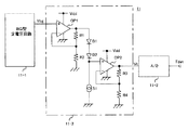
図1は本発明による液晶表示装置のための液晶駆動装置のシステム構成を示す図である。この液晶駆動装置はモジュール構成とされており、同一半導体基板内に形成されている。その主な構成部として、外部I/F回路1、駆動電圧等発生回路2、この発生回路2とともに駆動手段を構成する液晶駆動回路3、表示メモリ4、ドライバコントローラ5、設定レジスタ6、温度センサ11、昇圧回路12及び温度補正回路10を有している。なお、温度補正回路10は、ドライバコントローラ5に内蔵されることとして記載しているが、この他、駆動電圧等発生回路2に設けてもよいし、或いは、単独で別に設けることとしてもよい。また、昇圧回路12は、単独で別に設けることとして記載しているが、駆動電圧等発生回路2に含ませてもよい。また、図示省略しているが、タイミング発生回路等の必要な構成要素を有している。
【0017】
外部I/F回路1は、このモジュールの外部に設けられているMPUなどの制御装置とインターフェースを行う。液晶駆動回路3は、駆動電圧等発生回路2からの駆動電圧や、例えばRAMで構成される表示メモリ4の表示データを受けて、表示手段としての液晶表示パネル(図示していない)を駆動する。
【0018】
設定レジスタ6は、本液晶駆動装置の各種の設定値を格納するレジスタであり、ドライバの出力電圧値や表示モード、フレーム周波数等の種々の設定値が格納され、この設定値に基づいて各構成要素の動作条件が設定される。
【0019】
温度センサ11は、表示手段である液晶表示パネルに近接して設けられ、その温度を検出するセンサである。この温度センサ11も他の構成要素と同じ、同一半導体基板内に形成されており、例えば表示パネルのガラス面に、COG(チップ・オン・グラス)で設けられている。この温度センサ11は、ドライバコントローラ5から供給されるモニタ信号Mtに応じて動作を開始し、ディジタル温度データTdetを検出する。
【0020】
温度補正回路10は、温度センサ11で検出されたディジタル温度データが供給され、このディジタル温度データの変化に応じて液晶表示パネルの種々の駆動条件を、その変化前の旧駆動条件設定値からディジタル温度データに対応した変化後の新駆動条件設定値に設定変更する。
【0021】
昇圧回路12は、電源電圧Vddをチャージポンプ回路により昇圧して、出力電圧Voutを駆動電圧等発生回路2に供給する。この昇圧回路12としては、昇圧電圧が所定の値に達していることが検出された時は休止し、電力消費により所定の電圧より低下すると動作される第1のタイプのものと、オン・オフスイッチングによる昇圧動作を常時行わせる、第2のタイプのものとがある。この実施の形態では、第1のタイプの昇圧回路を用いている。
【0022】
ドライバコントローラ5は、本液晶駆動装置の各構成部を制御するものであり、外部のMPUからの初期設定データを設定レジスタ6に記憶させる等の作用を行う。この例ではさらに前述の温度補正回路10を有している。
【0023】
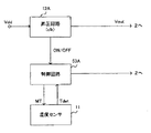
図2は、本発明の温度検出動作に特に関係する、温度センサ11、昇圧回路12及びドライバコントローラ5のブロック構成を示す図である。図3は、昇圧回路12の内部構成を示す部であり、また図4は温度センサ11の内部構成を示す図である。
【0024】
図2において、昇圧回路12で電源電圧Vddが昇圧された昇圧電圧Voutは、駆動電圧等発生回路2へ供給されるとともに、比較器52の反転入力端子(−)に供給される。基準電圧回路51は、例えばバンドギャップ型定電圧回路と電圧調整回路とからなり、制御回路53からの電圧指令データに基づいて調整回路を調整して所定の基準電圧Vrefを形成し、比較器52の非反転入力端子(+)に供給する。比較器52は、昇圧電圧Voutを基準電圧Vrefと比較し、その比較結果に応じて、イネーブル信号EN及びビジー信号Busyを発生する。イネーブル信号ENは昇圧回路12に供給されて、それを動作させる。制御回路53は、ビジー信号Busyのないときにモニタ信号Mtを温度センサ11に供給する。そして、温度センサ11からディジタル温度データTdetを受けて、制御回路53に内蔵されている温度補正回路10に供給する。
【0025】
昇圧回路12の内部構成を示す図3において、初段のチャージポンプユニットU1から出力段のチャージポンプユニットUnまでN段のチャージポンプユニットが直列に接続されている。初段のユニットU1に電源電圧Vdd(例えば、2Vや3Vなど)が供給される。また、出力段のユニットUnの出力側からは、ソースとゲートが接続された高耐圧用のN型MOSトランジスタ(スイッチ)Qoとそのドレイン側とグランド電位間に接続されたコンデンサCoとからなる出力平滑回路Uoを介して、電源電圧Vddが昇圧された所定の昇圧電圧Vout(例えば、10V)が出力される。
【0026】
各ユニットU1〜Unは、同様の構成であり、例えばユニットU1を例に説明すると、高耐圧用のN型MOSトランジスタQ1とコンデンサC1とを備えている。N型MOSトランジスタQ1のソースSは、電源電圧Vddが供給されるとともに、ゲートGに接続されており、いわゆるダイオード接続とされている。また、そのドレインDは次段のユニットU2のN型MOSトランジスタQ2のソースSに接続されており、その基板はもっとも低い電位点、この例ではグランド電位に接続されている。また、コンデンサC1は一端がドレインDに接続され、他端がクロックライン(この場合は、第1クロックCLK1のクロックライン)に接続される。
【0027】
なお、各ユニットのコンデンサは、奇数番のユニットU1,U3などでは第1クロックCLK1のクロックラインに接続され、偶数番のユニットU2,U4などでは第2クロックCLK2のクロックラインに接続される。
【0028】
第1クロックCLK1及び第2クロックCLK2は、例えば、電源電圧Vddと同じ振幅電圧で所定の周波数を持ち、ほぼ逆位相の状態で変化する二相クロックである。この第1クロックCLK1は、クロック信号clkが第1バッファB1で増幅されて出力される。また、第2クロックCLK2は、クロック信号clkが反転回路NOT1で反転され、第2バッファB2で増幅されて出力される。
【0029】
この図3の昇圧回路においては、イネーブル信号ENを受けて発振器OSCが発振を開始しクロック信号clkを発生する。このクロック信号clkは、例えば1MHzの高周波信号である。クロック信号clkがHレベル/Lレベルに交互に変化を開始すると、第1バッファB1及び反転回路NOT1・第2バッファB2により、第1クロックCLK1、第2クロックCLK2が、逆位相の状態で変化を開始する。
【0030】
この第1クロックCLK1、第2クロックCLK2の動作開始に応じて、各ユニットU1〜Unが同時にチャージポンプ動作を開始し、電源電圧Vddが各ユニット毎に順次チャージアップされ、昇圧電圧Voutが出力される。この昇圧回路12の動作中には、ユニットのチャージアップのために、電源ラインの電源電圧Vddやグランドラインの電圧が変動し、ノイズが発生する。
【0031】
また、図4の温度センサ11は、定電圧であるバンドギャップリフアレンス電圧Vbgを発生するバンドギャップ(以下、BG)型定電圧回路11−1と、BG電圧Vbgが入力され、周囲温度に応じた感温電圧Vtを出力する温度検出回路11−2と、感温電圧Vtをディジタル温度データTdetに変換するA/D変換回路11−3とから構成されている。
【0032】
BG型定電圧回路11−1は、ダイオードの電圧特性が負の温度係数を持つことを利用して正の温度係数となる電圧を発生させ、ダイオード自身の負の温度係数と打ち消すように構成して、温度の変化に影響されずに定電圧のBG電圧Vbgを出力する。
【0033】
温度検出回路11−2は、オペアンプOP1、抵抗R1、抵抗R2により非反転増幅回路が形成され、オペアンプOP1にBG電圧Vbgが加えられ、オペアンプOP1の出力端子にこの電圧を増幅した定電圧が得られる。この出力端子は、直列接続されたダイオードD1、D2を経て定電流源S1に接続しており、ダイオードD1、D2により定電圧を下げた電圧がオペアンプOP2に加えられる。オペアンプOP2、抵抗R3、抵抗R4は別の非反転増幅回路を形成しており、この回路は出力回路の役割をする。電流が一定のダイオードD1,D2の両端電圧は温度によって変化し、温度の上昇と共に小さくなる。したがって、ダイオードD1、D2により定電圧を下げることにより得られる電圧は温度の上昇と共に高くなり、その電圧が加えられるオペアンプOP2の出力に温度に対応する感温電圧Vtが得られる。
【0034】
A/D変換回路11−3は、入力されるアナログの感温電圧Vtを、例えば逐次型でディジタル信号に変換し、ディジタル温度データTdetを出力する。
【0035】
これらのBG型定電圧回路11−1及びA/D変換回路11−3は、温度変化に対してはそれほど影響を受けることなく安定して動作し、温度検出回路11−2は温度変化に応じた感温電圧Vtを出力する。ただ、それらの動作には電源電圧Vddが用いられ、またグランド電圧に接続されている。したがって、電源電圧やグランド電圧が変動したり、或いはそれらにノイズが重畳された場合には、それらの影響を受けて、出力すべきディジタル温度データTdetが誤差を含みやすくなる。
【0036】
さて、図1〜図4の本発明の実施の形態に係る表示装置の動作を、図5のタイミング図を参照して説明する。
【0037】
昇圧回路12の昇圧電圧Voutは、基準電圧発生回路51の基準電圧Vrefと比較器52で比較される。この比較器52は、安定した動作を行わせるために、例えば基準電圧Vrefを中心とした一定電圧のヒステリシス特性を持っている。したがって、昇圧電圧Voutは、その上限電圧Vout−uとその下限電圧Vout−dとの間にあるように制御される。
【0038】
図5の(i)の昇圧電圧Voutを見ると、最初はヒステリシス特性の上限電圧Vout−u側にある。この状態では比較器52の出力は低(L)レベルにあり、イネーブル信号EN(Hレベル)は出力されず、昇圧回路12は休止状態にある。
【0039】
液晶駆動回路3の駆動などにより電力が消費されると、昇圧電圧Voutは低下する。昇圧電圧Voutが時点t1で下限電圧Vout−dまで低下すると、比較器52の出力は反転して高(H)レベルになり、イネーブル信号ENが昇圧回路12に供給される。
【0040】
図3を参照して、イネーブル信号ENの供給により昇圧回路12の発振器OSCが発振を開始し、昇圧回路12は昇圧動作を開始する。この昇圧動作は発振器OSCのクロック信号clkにしたがって、電源電圧Vddをチャージアップし、昇圧電圧Voutが徐々に上昇していく。
【0041】
この昇圧電圧Voutのチャージアップ動作中は、コンデンサC1〜Cn、Coの充電、放電や、バッファB1,B2のオン/オフのスイッチングなどにより、図5の(iii)にノイズVnzで示されるように、電源ラインの電源電圧Vddやグランドラインの電圧が変動し、ノイズが発生する。このノイズVnzは昇圧回路12の動作中は発生し、更に動作終了後にも半導体基板電位の揺れが残るために短時間だけ継続して発生する。
【0042】
再び、図5を参照して、昇圧電圧Voutが徐々に上昇し、時点t2で上限電圧Vout−uまで上昇すると、比較器52の出力は反転してLレベルになり、イネーブル信号ENが停止する。昇圧回路12の動作は、以上の動作が時点t2〜t6に示されるように繰り返されて、ほぼ基準電圧Vrefに維持されるように制御される。
【0043】
一方、ビジー信号Busy(イネーブル信号と同じもの)が制御回路53に供給され、温度センサ11へのモニタ信号Mtを発生する。温度センサ11の各構成要素11−1〜11−3は、その動作に電源電圧Vddが用いられ、またグランド電圧に接続されているから、それらの変動やノイズの影響を受けて、出力すべきディジタル温度データTdetが誤差を含みやすくなる。
【0044】
この実施の形態では、ディジタル温度データTdetが誤差を含むことを避けるために、モニタ信号Mtは、図5の(iv)に示されるように、昇圧回路12の動作が終了して、更に半導体基板電位の揺れが収まる期間αだけ経過した時から、ディジタル温度データTdetが安定して得られるモニタ期間Tmだけ、出力される。
【0045】
このモニタ期間Tmは、例えばディジタル温度データTdetを複数回に亘って測定し、その平均値を得るに必要な時間とされる。昇圧回路12の休止期間はその動作期間とともに、その長さが不規則であるから、モニタ期間Tmは、通常もっとも短くなると想定される休止期間よりも、更に短く設定することになる。
【0046】
このモニタ期間Tm内に温度センサ11から取り込まれたディジタル温度データTdetは複数回に亘って平均化され、有意の平均値が得られた時点でその平均値をラッチし、当該休止期間での温度データとし、制御回路53内の温度補正回路10に供給する。なお、当該休止期間が必要な温度データを得るには短かった場合には、その回の温度データはキャンセルし、それ以前に得られているデータをそのまま使用するようにする。
【0047】
このように、昇圧回路12が休止しているときの温度センサ11の温度データを温度補正手段10での設定変更に用いるから、チャージポンプによる昇圧動作に伴って、電源ラインやグランドライン、及び信号ライン等に発生する電圧ノイズの影響を避けることができる。したがって、正確な温度データを用いて、温度補正を行うことができる。
【0048】
また、温度センサ11は、ノイズに影響されない期間で、温度データの必要なときにのみ発生されるモニタ信号Mtにしたがって動作するから、温度検出に要する消費電力を低減することができる。
その変形例として、モニタ信号Mtに応じて動作行うのは、比較的消費電力の大きい温度検出回路11−2及び/または、A/D変換回路11−3とし、安定した電圧を出力するのに多少時間を要するBG型定電圧回路11−1は常時動作させておいてもよい。これにより、高速応答と低消費電力とを両立させることができる。この点は、他の実施の形態でも同様である。
【0049】
更に、図5の(vi)に示されるように、温度センサ11の全体を常時連続的に動作させておくこともできる。この場合には、モニタ信号Mtを温度センサに供給することはなく、モニタ信号Mtに相当する期間に、温度センサ11から出力されるディジタル温度データTdetを制御回路に取り込むようにしてもよい。これによれば、温度センサ11は、常時動作しているから消費電力はその分だけ増加するが、必要なときに遅滞なく、温度データTdetを安定して得ることができる。この点も、他の実施の形態でも同様である。
【0050】
図6は、本発明の他の実施の形態に係る表示装置の温度検出動作に特に関係する、温度センサ11、昇圧回路12A及びドライバコントローラ5に含まれる制御回路53Aのブロック構成を示す図である。また、図7はその動作のタイミングを示す図である。なお、この他の実施の形態においても、図1の液晶駆動装置のシステム構成を示す図及び図4の温度センサの内部構成図は同じものが使用される。
【0051】
また、昇圧回路12Aは、第2のタイプの昇圧回路であり、発振器OSCが常時連続して発振している。したがってイネーブル信号ENは入力されず、代わりにクロック信号clkがオン・オフ信号ON/OFFとして出力される、点で図3の構成と異なる。また、図3の昇圧回路と比較して、コンデンサC1〜Cn、Coの静電容量が大きく、また、これに関連して、発振器OSCの発振周波数は1桁〜2桁低い周波数(100〜10kHz程度)とされている。
【0052】
さて、図6、図7を参照して本発明の他の実施の形態に係る表示装置の動作を説明する。
【0053】
昇圧回路12Aは連続して動作しているから、出力用のMOSトランジスタQoは図7の(ii)に示されるようにオン・オフされる。その昇圧電圧Voutは、図7の(i)に示されるように、出力用のMOSトランジスタQoがオン(即ち、バッファB1の出力が電源電圧Vdd)になった時点t1でコンデンサCoの充電を開始し、その電圧が上昇して、その充電能力まで充電された時点t2で上昇が終了する。その後は、消費される電力の大きさにしたがって、時間の経過とともに徐々に低下していく。この場合には、昇圧電圧Voutはフィードバック等により定電圧制御を行っていないので、昇圧電圧Voutの高さは負荷条件によって異なるが、コンデンサCoの静電容量が大きいものを使用するから、極端には変動しない。
【0054】
出力用のMOSトランジスタQoがオンして昇圧電圧Voutが上昇している期間t1〜t2はその供給源となっている電源電圧Vddやグランド電圧はその値が変動している。この実施の形態でも、ディジタル温度データTdetが誤差を含むことを避けるために、モニタ信号Mtを、図7の(iv)に示されるように、電源電圧Vddなどの変動する期間に余裕期間を付加した、待ち期間βの経過後に温度センサ11に供給する。モニタ信号Mtの期間Tmは、ディジタル温度データTdet(図7の(v))が安定して得られるモニタ期間Tmだけ、出力される。
【0055】
このモニタ期間Tm内に温度センサ11から取り込まれたディジタル温度データTdetは複数回に亘って平均化され、有意の平均値が得られた時点でその平均値をラッチし、温度データとし、制御回路53A内の温度補正回路10に供給する。
【0056】
なお、時点t3〜t4の期間は、出力用MOSトランジスタQoの前段のMOSトランジスタなどがオンすることによる電圧変動期間であり、この期間も避けて、同様に温度データを得る。
【0057】
このように、チャージポンプ型昇圧回路内のスイッチのスイッチング時及びその後の所定時間以外のモニタ期間Tm、即ち電源やグランドが安定しているときの温度センサ11の温度データを温度補正手段での設定変更に用いるから、昇圧動作に伴って、電源ラインやグランドライン、及び信号ライン等に発生する電圧変動や電圧ノイズの影響を避けることができる。したがって、正確な温度データを用いて、温度補正を行うことができる。
【0058】
【発明の効果】
請求項1記載の表示装置によれば、昇圧回路が休止しているときの温度センサの温度データを温度補正手段での設定変更に用いるから、昇圧動作に伴って、電源ラインやグランドライン、及び信号ライン等に発生する電圧ノイズの影響を避けることができる。したがって、正確な温度データを用いて、温度補正を行うことができる。
【0059】
請求項5記載の表示装置によれば、チャージポンプ型昇圧回路内のスイッチのスイッチング時及びその後の所定時間以外の期間、即ち電源やグランドが安定しているときの温度センサの温度データを温度補正手段での設定変更に用いるから、昇圧動作に伴って、電源ラインやグランドライン、及び信号ライン等に発生する電圧変動や電圧ノイズの影響を避けることができる。したがって、正確な温度データを用いて、温度補正を行うことができる。
【0060】
請求項2,3及び6,7記載の表示装置によれば、温度センサは、ノイズに影響されない期間で、かつ温度データの必要なときにのみ動作するから、温度検出に要する消費電力を低減することができる。
【0061】
請求項4、8記載の表示装置によれば、温度センサは、常時動作しているから消費電力はその分だけ増加するが、必要なときに遅滞なく、温度データを安定して得ることができる。
【図面の簡単な説明】
【図1】本発明の実施の形態に係るシステム構成を示す図。
【図2】本発明の実施の形態に係る温度検出動作に特に関係する部分のブロック構成を示す図。
【図3】昇圧回路の内部構成を示す図。
【図4】温度センサの内部構成を示す図。
【図5】本発明の実施の形態に係る表示装置のタイミング図。
【図6】本発明の他の実施の形態に係る温度検出動作に特に関係する部分のブロック構成を示す図。
【図7】本発明の他の実施の形態に係る表示装置のタイミング図。
【符号の説明】
1 外部I/F回路
2 駆動電圧等発生回路
3 液晶駆動回路
4 表示メモリ
5 ドライバコントローラ
6 設定レジスタ
10 温度補正回路
11 温度センサ
11−1 BG型定電圧回路
11−2 温度検出回路
11−3 A/D変換回路
12、12A 昇圧回路
51 基準電圧回路
52 比較器
53、53A 制御回路
Q1〜Qn、Qo MOSトランジスタ
C1〜Cn、Co コンデンサ
OSC 発振器
B1,B2 バッファ
NOT1 反転回路
OP1,OP2 オペアンプ
S1 定電流源
R1〜R4 抵抗[0001]
BACKGROUND OF THE INVENTION
The present invention relates to a display device using a display element whose display characteristics change depending on the ambient temperature, such as a liquid crystal display element or an organic EL display element, and more particularly to a display device in which drive conditions are changed according to the ambient temperature.
[0002]
[Prior art]
In display means such as a liquid crystal display system and an organic EL display system, a power supply voltage is boosted by a booster circuit to drive a display element to form a necessary drive voltage. In recent years, the display power of these display means has been improved, and the display means of small devices such as PDAs and mobile phones has also been improved in high resolution and multi-gradation (for example, monochrome gradation, number of color colors). Yes. In order to keep driving a liquid crystal display element and an organic EL display element (hereinafter, representatively referred to as a liquid crystal display element) under appropriate driving conditions during multi-tone driving, a liquid crystal display element that changes according to temperature is used. It is necessary to accurately follow the driving conditions such as threshold voltage and reaction time.
[0003]
For this reason, conventionally, as disclosed in Japanese Patent Laid-Open No. 5-273941, a temperature sensor is arranged in the vicinity of the liquid crystal display panel, and digital processing is performed based on the detected temperature of the temperature sensor to obtain a driving condition. The liquid crystal display panel is driven under the optimum conditions for the detected temperature.
[0004]
[Problems to be solved by the invention]
In the conventional liquid crystal display device, the temperature detected by the temperature sensor is measured as needed when temperature detection is required, and is performed regardless of the control operation of the booster circuit.
[0005]
The temperature sensor measures a detected temperature by capturing a minute change in circuit voltage or current due to a temperature change. When the booster circuit operates during measurement of the detected temperature, voltage noise is often applied to the power supply line, the ground line, the signal line, and the like due to switching associated with the boosting operation. In particular, in a display device in which a booster circuit, a temperature sensor, and other display drive circuits are formed in the same semiconductor substrate, voltage noise increases. Since this voltage noise becomes an error component of the measured detected temperature, accurate temperature correction cannot be performed. This voltage noise can be reduced by increasing the power supply capacity or making the power supply line or ground line thicker. However, this increases the cost of the display device and increases the space. Not right.
[0006]
Therefore, the present invention reduces the measurement error of the temperature sensor detection temperature without limiting the operation of the booster circuit in a display device having a booster circuit that generates a drive voltage and a temperature sensor that detects the temperature of the display panel. It is an object of the present invention to provide a display device that can be used.
[0007]
[Means for Solving the Problems]
The display device according to
[0008]
The display device according to
[0009]
The display device according to
[0010]
A display device according to a fourth aspect of the present invention is the display device according to the first aspect of the present invention, wherein the temperature sensor is operated continuously, and only the temperature data obtained by the booster circuit during a predetermined period of a pause period is obtained. It is used as temperature data for changing the setting to the new driving condition setting value.
[0011]
The display device according to
[0012]
The display device according to a sixth aspect of the present invention is the display device according to the fifth aspect of the present invention, wherein the temperature sensor is provided only during a predetermined period other than the predetermined time when the switch in the charge pump type booster circuit is switched and thereafter. It is characterized by operating.
[0013]
The display device according to claim 7 of the present invention is characterized in that, in the display device according to claim 6 of the present invention, the operation of the temperature sensor is further performed at regular intervals including a plurality of switching times.
[0014]
The display device according to an eighth aspect of the present invention is the display device according to the fifth aspect of the present invention, wherein the temperature sensor is continuously operated, and the switching in the switch of the charge pump type booster circuit is performed at a time other than a predetermined time thereafter. Only the temperature data of the period is used as temperature data for changing the setting to the new drive condition setting value.
[0015]
DETAILED DESCRIPTION OF THE INVENTION
Hereinafter, embodiments of the display device of the present invention will be described with reference to the drawings, taking a liquid crystal display device as an example.
[0016]
FIG. 1 is a diagram showing a system configuration of a liquid crystal driving device for a liquid crystal display device according to the present invention. This liquid crystal driving device has a module configuration and is formed in the same semiconductor substrate. The main components are an external I /
[0017]
The external I /
[0018]
The setting register 6 is a register for storing various setting values of the liquid crystal driving device, and stores various setting values such as an output voltage value of the driver, a display mode, a frame frequency, and the like. The operating condition of the element is set.
[0019]
The
[0020]
The temperature correction circuit 10 is supplied with the digital temperature data detected by the
[0021]
The
[0022]
The
[0023]
FIG. 2 is a diagram showing a block configuration of the
[0024]
In FIG. 2, the boosted voltage Vout obtained by boosting the power supply voltage Vdd by the
[0025]
In FIG. 3 showing the internal configuration of the
[0026]
The units U1 to Un have the same configuration. For example, when the unit U1 is described as an example, the unit U1 to Un includes a high breakdown voltage N-type MOS transistor Q1 and a capacitor C1. The source S of the N-type MOS transistor Q1 is supplied with the power supply voltage Vdd and is connected to the gate G, so-called diode connection. The drain D is connected to the source S of the N-type MOS transistor Q2 of the unit U2 in the next stage, and the substrate is connected to the lowest potential point, in this example, the ground potential. The capacitor C1 has one end connected to the drain D and the other end connected to the clock line (in this case, the clock line of the first clock CLK1).
[0027]
The capacitors of each unit are connected to the clock line of the first clock CLK1 in the odd-numbered units U1, U3 and the like, and are connected to the clock line of the second clock CLK2 in the even-numbered units U2, U4 and the like.
[0028]
The first clock CLK1 and the second clock CLK2 are, for example, two-phase clocks that have the same amplitude voltage as the power supply voltage Vdd, have a predetermined frequency, and change in an almost opposite phase. The first clock CLK1 is output after the clock signal clk is amplified by the first buffer B1. Further, the second clock CLK2 is output after the clock signal clk is inverted by the inverting circuit NOT1, amplified by the second buffer B2.
[0029]
In the booster circuit of FIG. 3, upon receiving the enable signal EN, the oscillator OSC starts oscillating and generates a clock signal clk. The clock signal clk is a high frequency signal of 1 MHz, for example. When the clock signal clk starts to change alternately between the H level and the L level, the first clock CLK1 and the second clock CLK2 change in opposite phases by the first buffer B1 and the inverting circuit NOT1 and the second buffer B2. Start.
[0030]
In response to the start of the operation of the first clock CLK1 and the second clock CLK2, the units U1 to Un start the charge pump operation simultaneously, the power supply voltage Vdd is sequentially charged up for each unit, and the boosted voltage Vout is output. The During the operation of the
[0031]
4 receives a bandgap (hereinafter referred to as BG) type constant voltage circuit 11-1 that generates a bandgap reference voltage Vbg, which is a constant voltage, and a BG voltage Vbg according to the ambient temperature. The temperature detection circuit 11-2 outputs the detected temperature sensing voltage Vt, and the A / D conversion circuit 11-3 converts the temperature sensing voltage Vt into the digital temperature data Tdet.
[0032]
The BG type constant voltage circuit 11-1 is configured to generate a voltage having a positive temperature coefficient by using the voltage characteristic of the diode having a negative temperature coefficient, and to cancel the negative temperature coefficient of the diode itself. Thus, a constant BG voltage Vbg is output without being affected by the change in temperature.
[0033]
In the temperature detection circuit 11-2, a non-inverting amplifier circuit is formed by the operational amplifier OP1, the resistor R1, and the resistor R2. The BG voltage Vbg is applied to the operational amplifier OP1, and a constant voltage obtained by amplifying this voltage is obtained at the output terminal of the operational amplifier OP1. It is done. This output terminal is connected to a constant current source S1 via diodes D1 and D2 connected in series, and a voltage obtained by lowering the constant voltage by the diodes D1 and D2 is applied to the operational amplifier OP2. The operational amplifier OP2, the resistor R3, and the resistor R4 form another non-inverting amplifier circuit, and this circuit serves as an output circuit. The voltage across the diodes D1 and D2 with constant current varies with temperature and decreases with increasing temperature. Therefore, the voltage obtained by lowering the constant voltage by the diodes D1 and D2 increases as the temperature rises, and a temperature-sensitive voltage Vt corresponding to the temperature is obtained at the output of the operational amplifier OP2 to which the voltage is applied.
[0034]
The A / D conversion circuit 11-3 converts the input analog temperature-sensitive voltage Vt into a digital signal, for example, in a sequential manner, and outputs digital temperature data Tdet.
[0035]
The BG type constant voltage circuit 11-1 and the A / D conversion circuit 11-3 operate stably without being affected so much by the temperature change, and the temperature detection circuit 11-2 responds to the temperature change. The temperature sensor voltage Vt is output. However, the power supply voltage Vdd is used for these operations and is connected to the ground voltage. Therefore, when the power supply voltage or the ground voltage fluctuates or noise is superimposed on them, the digital temperature data Tdet to be output tends to include an error due to the influence thereof.
[0036]
Now, the operation of the display device according to the embodiment of the present invention shown in FIGS. 1 to 4 will be described with reference to the timing chart of FIG.
[0037]
The boosted voltage Vout of the
[0038]
Looking at the boosted voltage Vout in (i) of FIG. 5, it is initially on the upper limit voltage Vout-u side of the hysteresis characteristic. In this state, the output of the
[0039]
When power is consumed by driving the liquid
[0040]
Referring to FIG. 3, the supply of enable signal EN causes oscillator OSC of
[0041]
During the charge-up operation of the boosted voltage Vout, as indicated by the noise Vnz in FIG. 5 (iii) due to the charging and discharging of the capacitors C1 to Cn and Co, the on / off switching of the buffers B1 and B2, and the like. The power supply voltage Vdd of the power supply line and the voltage of the ground line fluctuate, and noise is generated. This noise Vnz is generated during the operation of the
[0042]
Referring to FIG. 5 again, when boosted voltage Vout gradually rises and rises to upper limit voltage Vout-u at time t2, the output of
[0043]
On the other hand, a busy signal Busy (same as the enable signal) is supplied to the
[0044]
In this embodiment, in order to avoid that the digital temperature data Tdet includes an error, the monitor signal Mt is generated after the operation of the
[0045]
The monitoring period Tm is, for example, a time required to measure the digital temperature data Tdet a plurality of times and obtain an average value thereof. Since the length of the pause period of the
[0046]
The digital temperature data Tdet captured from the
[0047]
Thus, since the temperature data of the
[0048]
Further, since the
As a modified example, the temperature detection circuit 11-2 and / or the A / D conversion circuit 11-3, which operate relatively in response to the monitor signal Mt, outputs a stable voltage. The BG type constant voltage circuit 11-1 that requires some time may be always operated. Thereby, both high-speed response and low power consumption can be achieved. This is the same in other embodiments.
[0049]
Furthermore, as shown in FIG. 5 (vi), the
[0050]
FIG. 6 is a diagram showing a block configuration of the
[0051]
The
[0052]
Now, the operation of the display device according to another embodiment of the present invention will be described with reference to FIGS.
[0053]
Since the
[0054]
During the period t1 to t2 during which the output MOS transistor Qo is turned on and the boosted voltage Vout is rising, the values of the power supply voltage Vdd and the ground voltage serving as the supply source fluctuate. Also in this embodiment, in order to avoid that the digital temperature data Tdet includes an error, the monitor signal Mt is added with a margin period in a period in which the power supply voltage Vdd and the like fluctuate as shown in FIG. After the waiting period β, the
[0055]
The digital temperature data Tdet fetched from the
[0056]
Note that the period from the time point t3 to t4 is a voltage fluctuation period caused by turning on the MOS transistor or the like before the output MOS transistor Qo, and temperature data is similarly obtained while avoiding this period.
[0057]
In this way, the temperature correction means sets the temperature data of the
[0058]
【The invention's effect】
According to the display device of
[0059]
According to the display device of
[0060]
According to the display device of the second, third, sixth, and seventh aspects, the temperature sensor operates only in a period not affected by noise and when temperature data is necessary, and thus reduces power consumption required for temperature detection. be able to.
[0061]
According to the display device of the fourth and eighth aspects, since the temperature sensor is always operating, the power consumption is increased correspondingly, but the temperature data can be stably obtained without delay when necessary. .
[Brief description of the drawings]
FIG. 1 is a diagram showing a system configuration according to an embodiment of the present invention.
FIG. 2 is a diagram showing a block configuration of a portion particularly related to a temperature detection operation according to the embodiment of the present invention.
FIG. 3 is a diagram showing an internal configuration of a booster circuit.
FIG. 4 is a diagram showing an internal configuration of a temperature sensor.
FIG. 5 is a timing chart of the display device according to the embodiment of the present invention.
FIG. 6 is a diagram showing a block configuration of a portion particularly related to a temperature detection operation according to another embodiment of the present invention.
FIG. 7 is a timing chart of a display device according to another embodiment of the present invention.
[Explanation of symbols]
1 External I / F circuit
2 Driving voltage generation circuit
3 Liquid crystal drive circuit
4 Display memory
5 Driver controller
6 Setting register
10 Temperature correction circuit
11 Temperature sensor
11-1 BG type constant voltage circuit
11-2 Temperature detection circuit
11-3 A / D conversion circuit
12, 12A Booster circuit
51 Reference voltage circuit
52 Comparator
53, 53A Control circuit
Q1-Qn, Qo MOS transistors
C1-Cn, Co capacitors
OSC oscillator
B1, B2 buffer
NOT1 Inversion circuit
OP1, OP2 operational amplifier
S1 Constant current source
R1-R4 resistance
Claims (8)
この表示手段に表示すべき内容を記憶する表示メモリ手段と、
電源電圧を昇圧した所定値の昇圧電圧を駆動電圧源として出力するように動作及び休止を繰り返す昇圧回路を有し、前記表示手段に接続される駆動手段と、
前記表示手段の温度を検出し、前記昇圧回路が休止しているときの温度データを出力する温度センサと、
該温度センサから出力された温度データの変化に応じて前記表示手段の駆動条件を、その変化前の旧駆動条件設定値から前記温度データに対応した変化後の新駆動条件設定値に設定変更する温度補正手段と、
これら各手段と結合され、それらを制御するコントローラ部とを備えることを特徴とする、表示装置。Display means;
Display memory means for storing contents to be displayed on the display means;
A drive unit having a booster circuit that repeats operation and pause so as to output a boosted voltage of a predetermined value obtained by boosting the power supply voltage as a drive voltage source; and a drive unit connected to the display unit;
A temperature sensor for detecting the temperature of the display means and outputting temperature data when the booster circuit is at rest;
In accordance with a change in temperature data output from the temperature sensor, the driving condition of the display means is changed from the old driving condition setting value before the change to the new driving condition setting value after the change corresponding to the temperature data. Temperature correction means;
A display device comprising: a controller unit coupled to each of these means and controlling them.
この表示手段に表示すべき内容を記憶する表示メモリ手段と、
電源電圧を昇圧した昇圧電圧を駆動電圧源として出力するように連続的に動作するチャージポンプ型昇圧回路を有し、前記表示手段に接続される駆動手段と、
前記表示手段の温度を検出し、前記チャージポンプ型昇圧回路内のスイッチのスイッチング時及びその後の所定時間以外の期間における温度データを出力する温度センサと、
該温度センサから出力された温度データの変化に応じて前記表示手段の駆動条件を、その変化前の旧駆動条件設定値から前記温度データに対応した変化後の新駆動条件設定値に設定変更する温度補正手段と、
これら各手段と結合され、それらを制御するコントローラ部とを備えることを特徴とする、表示装置。Display means;
Display memory means for storing contents to be displayed on the display means;
Drive means connected to the display means, having a charge pump type booster circuit operating continuously so as to output a boosted voltage obtained by boosting the power supply voltage as a drive voltage source;
A temperature sensor that detects the temperature of the display means and outputs temperature data at a time other than a predetermined time after switching of the switch in the charge pump booster circuit; and
In accordance with a change in temperature data output from the temperature sensor, the driving condition of the display means is changed from the old driving condition setting value before the change to the new driving condition setting value after the change corresponding to the temperature data. Temperature correction means;
A display device comprising: a controller unit coupled to each of these means and controlling them.
Priority Applications (4)
| Application Number | Priority Date | Filing Date | Title |
|---|---|---|---|
| JP2002246325A JP3887285B2 (en) | 2002-08-27 | 2002-08-27 | Display device |
| US10/641,460 US7038654B2 (en) | 2002-08-27 | 2003-08-14 | Display apparatus having temperature compensation function |
| CNB031553508A CN100375134C (en) | 2002-08-27 | 2003-08-27 | Display device with temperature compensating function |
| US11/356,745 US7466300B2 (en) | 2002-08-27 | 2006-02-17 | Display apparatus having temperature compensation function |
Applications Claiming Priority (1)
| Application Number | Priority Date | Filing Date | Title |
|---|---|---|---|
| JP2002246325A JP3887285B2 (en) | 2002-08-27 | 2002-08-27 | Display device |
Publications (2)
| Publication Number | Publication Date |
|---|---|
| JP2004085858A JP2004085858A (en) | 2004-03-18 |
| JP3887285B2 true JP3887285B2 (en) | 2007-02-28 |
Family
ID=31972412
Family Applications (1)
| Application Number | Title | Priority Date | Filing Date |
|---|---|---|---|
| JP2002246325A Expired - Fee Related JP3887285B2 (en) | 2002-08-27 | 2002-08-27 | Display device |
Country Status (3)
| Country | Link |
|---|---|
| US (2) | US7038654B2 (en) |
| JP (1) | JP3887285B2 (en) |
| CN (1) | CN100375134C (en) |
Families Citing this family (35)
| Publication number | Priority date | Publication date | Assignee | Title |
|---|---|---|---|---|
| JP2005031430A (en) * | 2003-07-14 | 2005-02-03 | Tohoku Pioneer Corp | Method and device for driving light emitting display panel |
| US8358296B2 (en) * | 2004-01-13 | 2013-01-22 | Hewlett-Packard Development Company, L.P. | Temperature compensated MEMS device |
| US20060007207A1 (en) * | 2004-04-01 | 2006-01-12 | Toshiba Matsushita Display Technology Co., Ltd. | Liquid crystal display device and method of driving liquid crystal display device |
| JP4771043B2 (en) * | 2004-09-06 | 2011-09-14 | 日本電気株式会社 | Thin film semiconductor device, driving circuit thereof, and apparatus using them |
| KR100586997B1 (en) * | 2004-10-07 | 2006-06-08 | 삼성전자주식회사 | Driving Method for Display Panel And Control Method Thereof |
| JP5034182B2 (en) * | 2005-07-22 | 2012-09-26 | カシオ計算機株式会社 | Voltage supply circuit |
| US7639222B2 (en) * | 2005-10-04 | 2009-12-29 | Chunghwa Picture Tubes, Ltd. | Flat panel display, image correction circuit and method of the same |
| KR101193111B1 (en) | 2005-10-18 | 2012-10-22 | 삼성디스플레이 주식회사 | Circuit for generating temperature compensated driving voltage and liquid crystal display device having the same and method for generating driving voltage |
| US20070085807A1 (en) * | 2005-10-19 | 2007-04-19 | Rosemount Inc. | LCD design for cold temperature operation |
| KR100734311B1 (en) * | 2006-02-07 | 2007-07-02 | 삼성전자주식회사 | Apparatus and method for driving a display panel by compensating temperature |
| CN101401026B (en) * | 2006-04-19 | 2013-04-24 | 夏普株式会社 | Liquid crystal display device and its driving method, and drive circuit |
| TWI350517B (en) * | 2006-09-22 | 2011-10-11 | Chimei Innolux Corp | Display device |
| JP5112753B2 (en) * | 2007-06-08 | 2013-01-09 | セイコーインスツル株式会社 | Charge pump circuit |
| TW200849784A (en) * | 2007-06-12 | 2008-12-16 | Vastview Tech Inc | DC-DC converter with temperature compensation circuit |
| US8212760B2 (en) * | 2007-07-19 | 2012-07-03 | Chimei Innolux Corporation | Digital driving method for LCD panels |
| DE102007035418A1 (en) | 2007-07-28 | 2009-01-29 | Vastview Technology Inc. | Direct current converter for electronic device, has circuit with current source, and producing compensation voltage, which is superimposed to regulate voltage level of output direct current voltage |
| US20090284513A1 (en) * | 2008-05-19 | 2009-11-19 | Paul Fredrick Weindorf | Liquid crystal display control system and method |
| KR100957936B1 (en) * | 2008-07-18 | 2010-05-13 | 삼성모바일디스플레이주식회사 | Liquid Crystal Display Device and Driving Method Thereof |
| US20100079128A1 (en) * | 2008-09-30 | 2010-04-01 | Apple Inc. | Low noise external enable switcher control signal using on-chip switcher |
| US8159448B2 (en) * | 2008-12-19 | 2012-04-17 | Analog Devices, Inc. | Temperature-compensation networks |
| US20110248969A1 (en) * | 2010-04-08 | 2011-10-13 | Samsung Electronics Co., Ltd. | Lcd display apparatus and lcd driving method |
| CN101944321B (en) * | 2010-09-26 | 2012-11-21 | 友达光电股份有限公司 | Grid drive pulse compensation circuit and display device |
| KR101745418B1 (en) * | 2010-12-30 | 2017-06-12 | 엘지디스플레이 주식회사 | Power supply unit and liquid crystal display device including the same |
| JP2012226062A (en) * | 2011-04-19 | 2012-11-15 | Canon Inc | Reflection type liquid crystal display element and image display device |
| CN102368381A (en) * | 2011-10-27 | 2012-03-07 | 深圳市华星光电技术有限公司 | Method for improving charging of liquid crystal panel and circuit thereof |
| JP5962127B2 (en) * | 2012-03-29 | 2016-08-03 | セイコーエプソン株式会社 | Integrated circuit device, electro-optical device and electronic apparatus |
| TWI488170B (en) * | 2012-04-11 | 2015-06-11 | Sitronix Technology Corp | Display the drive circuit of the panel |
| WO2014016867A1 (en) * | 2012-07-24 | 2014-01-30 | ルネサスモバイル株式会社 | Semiconductor device and electronic apparatus |
| CN103023325B (en) * | 2012-12-06 | 2015-11-25 | 北京控制工程研究所 | Low-power-consumptiocontrol control method and circuit |
| JP6330396B2 (en) * | 2014-03-18 | 2018-05-30 | セイコーエプソン株式会社 | Display driver, electro-optical device, and electronic device |
| CN104036740B (en) * | 2014-05-16 | 2017-04-19 | 京东方科技集团股份有限公司 | Control circuit of gate driving circuit, working method and display device |
| US10250252B2 (en) * | 2016-11-03 | 2019-04-02 | Semiconductor Components Industries, Llc | Control circuit and method therefor |
| KR102548857B1 (en) * | 2016-11-30 | 2023-06-29 | 삼성디스플레이 주식회사 | Display apparatus and method of driving display panel using the same |
| WO2018104824A1 (en) * | 2016-12-07 | 2018-06-14 | Semiconductor Energy Laboratory Co., Ltd. | Semiconductor device, display system, and electronic device |
| US11450355B1 (en) * | 2021-05-03 | 2022-09-20 | Powerchip Semiconductor Manufacturing Corporation | Semiconductor memory with temperature dependence |
Family Cites Families (7)
| Publication number | Priority date | Publication date | Assignee | Title |
|---|---|---|---|---|
| JPH0833710B2 (en) * | 1991-06-28 | 1996-03-29 | 株式会社テイ・アイ・シイ・シチズン | Color display element and color display unit |
| JP3489169B2 (en) * | 1993-02-25 | 2004-01-19 | セイコーエプソン株式会社 | Driving method of liquid crystal display device |
| JPH10148808A (en) * | 1996-11-18 | 1998-06-02 | Seiko Epson Corp | Backlight device and liquid crystal display device using it |
| JP3342341B2 (en) * | 1997-03-13 | 2002-11-05 | キヤノン株式会社 | Liquid crystal device and driving method of liquid crystal device |
| JP3693464B2 (en) * | 1997-05-22 | 2005-09-07 | ローム株式会社 | Display panel drive device |
| JP3583265B2 (en) * | 1997-09-12 | 2004-11-04 | 株式会社リコー | Driving method of liquid crystal display element and liquid crystal display device |
| US6803899B1 (en) * | 1999-07-27 | 2004-10-12 | Minolta Co., Ltd. | Liquid crystal display apparatus and a temperature compensation method therefor |
-
2002
- 2002-08-27 JP JP2002246325A patent/JP3887285B2/en not_active Expired - Fee Related
-
2003
- 2003-08-14 US US10/641,460 patent/US7038654B2/en not_active Expired - Fee Related
- 2003-08-27 CN CNB031553508A patent/CN100375134C/en not_active Expired - Fee Related
-
2006
- 2006-02-17 US US11/356,745 patent/US7466300B2/en not_active Expired - Fee Related
Also Published As
| Publication number | Publication date |
|---|---|
| JP2004085858A (en) | 2004-03-18 |
| US20060139296A1 (en) | 2006-06-29 |
| US7466300B2 (en) | 2008-12-16 |
| US20040041762A1 (en) | 2004-03-04 |
| CN1489124A (en) | 2004-04-14 |
| US7038654B2 (en) | 2006-05-02 |
| CN100375134C (en) | 2008-03-12 |
Similar Documents
| Publication | Publication Date | Title |
|---|---|---|
| JP3887285B2 (en) | Display device | |
| US20060132417A1 (en) | Semiconductor integrated circuit for liquid crystal display driver | |
| KR101385229B1 (en) | Gate on voltage generator, driving device and display apparatus comprising the same | |
| JP5011478B2 (en) | Display device | |
| US8477123B2 (en) | Display apparatus, driving method thereof and electronic equipment including a drive circuit selectively driving scan lines and capacitor lines | |
| EP1376529B1 (en) | Image display device and portable electrical equipment | |
| US8730146B2 (en) | Drive voltage generating circuit and liquid crystal display including the same | |
| JP4964576B2 (en) | Voltage booster, voltage buck-boost device, and liquid crystal display device | |
| JP2011043843A (en) | Drive voltage control device | |
| JP2000137247A (en) | Active matrix liquid crystal display device | |
| US20080122812A1 (en) | Direct current to direct current converting circuit, display apparatus having the same and method of driving the direct current to direct current converting circuit | |
| US20090174372A1 (en) | Analog Output Circuit, Data Signal Line Driving Circuit, Display, and Potential Writing Method | |
| CN105938709B (en) | Driver, electro-optical device, and electronic apparatus | |
| US8791936B2 (en) | LCD module and method for adjusting response time period thereof | |
| JP2015035706A (en) | Method for controlling oscillation circuit, oscillating circuit, oscillator, electronic apparatus, and mobile body | |
| JP2009236603A (en) | Temperature sensor, manufacturing method of temperature sensor, electrophoretic device, and electronic device | |
| KR102385627B1 (en) | Power Supply Device, Display Device using the same and Driving Method thereof | |
| US20050180227A1 (en) | Booster circuit | |
| US11290013B2 (en) | Integrated circuit apparatus including regulator circuits | |
| JP2002090480A (en) | Clock signal supply device and its control method | |
| JP2001282189A (en) | Liquid crystal display device | |
| US10921195B2 (en) | Temperature sensor and temperature detection method | |
| JP2007199210A (en) | Semiconductor integrated circuit | |
| JP2009236605A (en) | Temperature sensor, manufacturing method of temperature sensor, electrophoretic device, and electronic device | |
| JP2004341543A (en) | Driver ic, electrooptical apparatus, and electronic device |
Legal Events
| Date | Code | Title | Description |
|---|---|---|---|
| A621 | Written request for application examination |
Free format text: JAPANESE INTERMEDIATE CODE: A621 Effective date: 20041014 |
|
| A977 | Report on retrieval |
Free format text: JAPANESE INTERMEDIATE CODE: A971007 Effective date: 20061026 |
|
| TRDD | Decision of grant or rejection written | ||
| A01 | Written decision to grant a patent or to grant a registration (utility model) |
Free format text: JAPANESE INTERMEDIATE CODE: A01 Effective date: 20061121 |
|
| A61 | First payment of annual fees (during grant procedure) |
Free format text: JAPANESE INTERMEDIATE CODE: A61 Effective date: 20061124 |
|
| R150 | Certificate of patent or registration of utility model |
Free format text: JAPANESE INTERMEDIATE CODE: R150 |
|
| FPAY | Renewal fee payment (event date is renewal date of database) |
Free format text: PAYMENT UNTIL: 20091201 Year of fee payment: 3 |
|
| FPAY | Renewal fee payment (event date is renewal date of database) |
Free format text: PAYMENT UNTIL: 20101201 Year of fee payment: 4 |
|
| FPAY | Renewal fee payment (event date is renewal date of database) |
Free format text: PAYMENT UNTIL: 20111201 Year of fee payment: 5 |
|
| LAPS | Cancellation because of no payment of annual fees |