EP0862204A1 - Method for fabricating a capacitor for a semiconductor structure - Google Patents
Method for fabricating a capacitor for a semiconductor structure Download PDFInfo
- Publication number
- EP0862204A1 EP0862204A1 EP98101832A EP98101832A EP0862204A1 EP 0862204 A1 EP0862204 A1 EP 0862204A1 EP 98101832 A EP98101832 A EP 98101832A EP 98101832 A EP98101832 A EP 98101832A EP 0862204 A1 EP0862204 A1 EP 0862204A1
- Authority
- EP
- European Patent Office
- Prior art keywords
- layers
- germanium
- layer
- doped silicon
- silicon
- Prior art date
- Legal status (The legal status is an assumption and is not a legal conclusion. Google has not performed a legal analysis and makes no representation as to the accuracy of the status listed.)
- Withdrawn
Links
- 239000003990 capacitor Substances 0.000 title claims abstract description 56
- 238000000034 method Methods 0.000 title claims description 23
- 239000004065 semiconductor Substances 0.000 title claims description 10
- XUIMIQQOPSSXEZ-UHFFFAOYSA-N Silicon Chemical compound [Si] XUIMIQQOPSSXEZ-UHFFFAOYSA-N 0.000 claims abstract description 61
- 229910052710 silicon Inorganic materials 0.000 claims abstract description 59
- 239000010703 silicon Substances 0.000 claims abstract description 58
- 229910052732 germanium Inorganic materials 0.000 claims abstract description 39
- GNPVGFCGXDBREM-UHFFFAOYSA-N germanium atom Chemical compound [Ge] GNPVGFCGXDBREM-UHFFFAOYSA-N 0.000 claims abstract description 39
- 239000000758 substrate Substances 0.000 claims description 27
- 229910021420 polycrystalline silicon Inorganic materials 0.000 claims description 21
- 229920005591 polysilicon Polymers 0.000 claims description 20
- 238000000151 deposition Methods 0.000 claims description 10
- 230000008021 deposition Effects 0.000 claims description 9
- 238000000407 epitaxy Methods 0.000 claims description 7
- 238000004519 manufacturing process Methods 0.000 claims description 6
- 238000011065 in-situ storage Methods 0.000 claims description 5
- 239000004020 conductor Substances 0.000 claims description 3
- 230000015654 memory Effects 0.000 abstract description 17
- 238000003860 storage Methods 0.000 description 27
- 238000005530 etching Methods 0.000 description 16
- 229910004298 SiO 2 Inorganic materials 0.000 description 6
- 238000009792 diffusion process Methods 0.000 description 5
- 238000000926 separation method Methods 0.000 description 5
- 230000015572 biosynthetic process Effects 0.000 description 4
- BLRPTPMANUNPDV-UHFFFAOYSA-N Silane Chemical compound [SiH4] BLRPTPMANUNPDV-UHFFFAOYSA-N 0.000 description 3
- VYPSYNLAJGMNEJ-UHFFFAOYSA-N Silicium dioxide Chemical compound O=[Si]=O VYPSYNLAJGMNEJ-UHFFFAOYSA-N 0.000 description 3
- 238000002955 isolation Methods 0.000 description 3
- 125000000896 monocarboxylic acid group Chemical group 0.000 description 3
- 238000012856 packing Methods 0.000 description 3
- 229910000077 silane Inorganic materials 0.000 description 3
- 229910052814 silicon oxide Inorganic materials 0.000 description 3
- OKTJSMMVPCPJKN-UHFFFAOYSA-N Carbon Chemical compound [C] OKTJSMMVPCPJKN-UHFFFAOYSA-N 0.000 description 2
- XYFCBTPGUUZFHI-UHFFFAOYSA-N Phosphine Chemical compound P XYFCBTPGUUZFHI-UHFFFAOYSA-N 0.000 description 2
- 229910052581 Si3N4 Inorganic materials 0.000 description 2
- 229910052799 carbon Inorganic materials 0.000 description 2
- PZPGRFITIJYNEJ-UHFFFAOYSA-N disilane Chemical compound [SiH3][SiH3] PZPGRFITIJYNEJ-UHFFFAOYSA-N 0.000 description 2
- 239000002019 doping agent Substances 0.000 description 2
- 239000000463 material Substances 0.000 description 2
- 239000000203 mixture Substances 0.000 description 2
- HQVNEWCFYHHQES-UHFFFAOYSA-N silicon nitride Chemical compound N12[Si]34N5[Si]62N3[Si]51N64 HQVNEWCFYHHQES-UHFFFAOYSA-N 0.000 description 2
- WFKWXMTUELFFGS-UHFFFAOYSA-N tungsten Chemical compound [W] WFKWXMTUELFFGS-UHFFFAOYSA-N 0.000 description 2
- 229910052721 tungsten Inorganic materials 0.000 description 2
- 239000010937 tungsten Substances 0.000 description 2
- WQJQOUPTWCFRMM-UHFFFAOYSA-N tungsten disilicide Chemical compound [Si]#[W]#[Si] WQJQOUPTWCFRMM-UHFFFAOYSA-N 0.000 description 2
- 229910021342 tungsten silicide Inorganic materials 0.000 description 2
- ZOXJGFHDIHLPTG-UHFFFAOYSA-N Boron Chemical compound [B] ZOXJGFHDIHLPTG-UHFFFAOYSA-N 0.000 description 1
- RTAQQCXQSZGOHL-UHFFFAOYSA-N Titanium Chemical compound [Ti] RTAQQCXQSZGOHL-UHFFFAOYSA-N 0.000 description 1
- NRTOMJZYCJJWKI-UHFFFAOYSA-N Titanium nitride Chemical compound [Ti]#N NRTOMJZYCJJWKI-UHFFFAOYSA-N 0.000 description 1
- RBFQJDQYXXHULB-UHFFFAOYSA-N arsane Chemical compound [AsH3] RBFQJDQYXXHULB-UHFFFAOYSA-N 0.000 description 1
- 229910052796 boron Inorganic materials 0.000 description 1
- OEYIOHPDSNJKLS-UHFFFAOYSA-N choline Chemical compound C[N+](C)(C)CCO OEYIOHPDSNJKLS-UHFFFAOYSA-N 0.000 description 1
- 229960001231 choline Drugs 0.000 description 1
- 238000001816 cooling Methods 0.000 description 1
- 239000011810 insulating material Substances 0.000 description 1
- 238000009413 insulation Methods 0.000 description 1
- 230000010354 integration Effects 0.000 description 1
- 239000004922 lacquer Substances 0.000 description 1
- 238000001459 lithography Methods 0.000 description 1
- 229910021421 monocrystalline silicon Inorganic materials 0.000 description 1
- 230000003647 oxidation Effects 0.000 description 1
- 238000007254 oxidation reaction Methods 0.000 description 1
- 229910000073 phosphorus hydride Inorganic materials 0.000 description 1
- 238000002360 preparation method Methods 0.000 description 1
- 230000000717 retained effect Effects 0.000 description 1
- 125000006850 spacer group Chemical group 0.000 description 1
- 239000000126 substance Substances 0.000 description 1
- 229910052715 tantalum Inorganic materials 0.000 description 1
- GUVRBAGPIYLISA-UHFFFAOYSA-N tantalum atom Chemical compound [Ta] GUVRBAGPIYLISA-UHFFFAOYSA-N 0.000 description 1
- 229910052719 titanium Inorganic materials 0.000 description 1
- 239000010936 titanium Substances 0.000 description 1
Images


Classifications
-
- H—ELECTRICITY
- H01—ELECTRIC ELEMENTS
- H01L—SEMICONDUCTOR DEVICES NOT COVERED BY CLASS H10
- H01L29/00—Semiconductor devices adapted for rectifying, amplifying, oscillating or switching, or capacitors or resistors with at least one potential-jump barrier or surface barrier, e.g. PN junction depletion layer or carrier concentration layer; Details of semiconductor bodies or of electrodes thereof ; Multistep manufacturing processes therefor
- H01L29/66—Types of semiconductor device ; Multistep manufacturing processes therefor
- H01L29/86—Types of semiconductor device ; Multistep manufacturing processes therefor controllable only by variation of the electric current supplied, or only the electric potential applied, to one or more of the electrodes carrying the current to be rectified, amplified, oscillated or switched
- H01L29/92—Capacitors with potential-jump barrier or surface barrier
- H01L29/94—Metal-insulator-semiconductors, e.g. MOS
-
- H—ELECTRICITY
- H10—SEMICONDUCTOR DEVICES; ELECTRIC SOLID-STATE DEVICES NOT OTHERWISE PROVIDED FOR
- H10B—ELECTRONIC MEMORY DEVICES
- H10B12/00—Dynamic random access memory [DRAM] devices
- H10B12/01—Manufacture or treatment
- H10B12/02—Manufacture or treatment for one transistor one-capacitor [1T-1C] memory cells
- H10B12/03—Making the capacitor or connections thereto
- H10B12/033—Making the capacitor or connections thereto the capacitor extending over the transistor
-
- H—ELECTRICITY
- H10—SEMICONDUCTOR DEVICES; ELECTRIC SOLID-STATE DEVICES NOT OTHERWISE PROVIDED FOR
- H10B—ELECTRONIC MEMORY DEVICES
- H10B12/00—Dynamic random access memory [DRAM] devices
- H10B12/30—DRAM devices comprising one-transistor - one-capacitor [1T-1C] memory cells
- H10B12/31—DRAM devices comprising one-transistor - one-capacitor [1T-1C] memory cells having a storage electrode stacked over the transistor
- H10B12/318—DRAM devices comprising one-transistor - one-capacitor [1T-1C] memory cells having a storage electrode stacked over the transistor the storage electrode having multiple segments
Definitions
- a single transistor memory cell of a dynamic semiconductor memory device comprises a read transistor and a capacitor.
- the information is stored in the form of an electrical charge, which is a logical quantity, zero or one.
- By driving the read transistor via a word line can read this information over a bit line will.
- Capacitor have a minimum capacitance. The lower limit for the capacity of the storage capacitor is currently seen at 25 fF.
- both the readout transistor as well as the capacitor as planar components Up to the 1MBit generation, both the readout transistor as well as the capacitor as planar components. From the 4MBit memory generation, there was a further reduction in area the memory cell by a three-dimensional arrangement achieved by read transistor and storage capacitor.
- One way to do this is to use the storage capacitor to be realized in a trench (see for example K. Yamada et al, Proc. Intern. Electronic devices and materials IEDM 85, page 702 ff).
- the electrodes of the storage capacitor are in this case along the surface of the trench arranged. This will reduce the effective area of the storage capacitor, on which the capacity depends the space requirement on the surface of the substrate for the storage capacitor, which corresponds to the cross section of the trench, enlarged.
- the storage capacitor as a stacked capacitor, the so-called stacked capacitor, to execute.
- a structure is created over the word lines made of polysilicon, for example a crown structure or a Cylinder formed, which is contacted with the substrate.
- This polysilicon structure forms the storage node. He will provided with capacitor dielectric and capacitor plate.
- This concept has the advantage that it is largely with one Logic process is compatible.
- the free space above the substrate surface is used.
- cover the entire cell area from the polysilicon structure be covered as long as the polysilicon structures to neighboring ones Memory cells are isolated from each other.
- a memory cell arrangement with a stacked capacitor as a storage capacitor is known from EP 0 415 530 B1.
- the stacked capacitor comprises a polysilicon structure with a plurality of polysilicon layers arranged essentially one above the other, which are connected to one another via at least one lateral support. These layers arranged in the form of a cooling fin lead to a significant increase in the surface of the polysilicon structure compared to the projection of the polysilicon structure onto the substrate surface.
- the polysilicon structure is formed by alternating deposition of polysilicon layers and selectively etchable SiO 2 or carbon layers on the surface of the substrate, structuring of these layers, generation of flank coverings (spacers made of polysilicon) on at least one flank of the layer structure and selective etching out of the SiO 2 or Carbon layers formed.
- the polysilicon structures are arsenic-doped.
- silicon oxide is formed as a capacitor dielectric by thermal oxidation, on which a cell plate made of doped polysilicon is deposited.
- GB 2 285 338 A describes a method for producing a Capacitor known, in which alternating on a substrate Layers of doped and undoped silicon are applied will. A contact hole is opened through the layers, that extends into an underlying substrate. The entire surface is covered with an undoped silicon layer covered. After structuring the layer sequence, the Flanks of the layers made of doped or undoped silicon free. The doped silicon layers become selective to the undoped silicon layers removed. The resulting one Silicon structure is doped by diffusion and as an electrode of the capacitor used.
- the invention is based on the problem of a method for Manufacture of a capacitor for a semiconductor device, Specify in particular for a DRAM arrangement in which the known solutions reduced the process effort becomes.
- the capacitor should at least in the the 1 GBit generation required packing density can be produced be.
- the layer sequence is structured in such a way that at least one layer structure with reaching down to the substrate Flanks arises. It becomes a support structure conductive material formed at least the flanks of the Layered structure covered.
- the support structure is made by selective Epitaxy formed by silicon. Preferably the Support structure endowed in situ.
- the layer structure then at least one opening is formed in which the Surface of the layers of doped silicon and the germanium-containing Layers exposed. Then the layers containing germanium selective to the layers of doped Silicon and the support structure removed.
- the exposed one Surface of the layers of doped silicon and the Support structure is provided with a capacitor dielectric. On the surface of the capacitor dielectric is a Counter electrode formed.
- the support structure is when etching out the germanium-containing Layers preferably on at least three flanks of the Layer structure arranged. This creates a high mechanical Stability guaranteed by sticking together the layers of doped silicon when etching out the layers of germanium from the second material avoided becomes. Because this mechanical stability through the support structure is guaranteed, the layer thickness of the layers made of doped silicon regardless of mechanical stability requirements to the layers of doped silicon to get voted.
- the layers of doped silicon can realized in particular in the thickness range between 20 and 50 nm will. This will also increase the total height of the capacitor reduced with the same capacity.
- the layers of doped silicon can be both polycrystalline as well as being crystalline or amorphous.
- germanium Layers of pure germanium or of silicon and germanium to build are made of silicon and germanium formed, the germanium content is preferably between 10 percent and 100 percent. The silicon content is between 0 percent and 90 percent.
- the layers containing germanium can be deposited both doped and undoped.
- Germanium-containing layers of pure germanium or of silicon and germanium can be etched wet-chemically with good selectivity to silicon. If an etching mixture containing HF, H 2 O 2 and CH 3 COOH is used, the selectivity of the etching to silicon is 1:30 to 1: 1000. With this etching, the selectivity to silicon oxide and silicon nitride is approximately 1:30 to 1: 1000.
- silicon layers can be selectively converted to germanium etching.
- the layer sequence remains unchanged even at process-related temperature loads of, for example, 800 ° C.
- the diffusion coefficients at a process temperature of 1000 ° C are approximately 1.5 x 10 -6 cm 2 / sec. For comparison: these diffusion coefficients are about 10 times lower than the diffusion coefficient of boron in silicon.
- the layers are preferably made of doped silicon a CVD process using silane as process gas in the Temperature range between 400 and 600 ° C at a pressure between 10 and 400 torr and a silane flow of 30 to 300 sccm with deposition rates of 10 to 100 nm per minute.
- the Germanium-containing layers are preferably by CVD deposition using German or German and Disilan in the process gas at a temperature between 400 and 600 ° C and a pressure between 10 and 400 Torr, the German river and possibly the disilane flow between 30 and 300 sccm is set and the deposition rate between 10 and is 100 nm per minute.
- the doped silicon layers are preferably in situ endowed deposited.
- the deposition becomes a doping gas, for example arsine, phosphine or diborane.
- the layers made of doped silicon and the support structure can both formed from n-doped as well as from p-doped silicon will.
- Doped silicon and germanium can be in the same reactor be deposited. This enables the layer sequence to be changed without changing the system only realized by switching the process parameters will. This means a significant process simplification.
- the support structure is provided with defined surfaces on the Flanks of the layer structure are formed. This ensures that the germanium-containing layers evenly between the layers of doped silicon are etched out. This prevents the germanium-containing Layers are not yet etched out locally and at the same time in other places the supporting surfaces were already so badly attacked that individual layers of doped silicon falling off.
- the layer structure and the support structure in divided into two sections by one down to the surface of the substrate-extending gap are spaced.
- Out Two capacitors are formed in the two sections.
- the distance and the structure size of the sub-areas can each corresponding to the minimum structure size F in the respective technology. This makes a high one Packing density achieved.
- the substrate When manufacturing the capacitor as a storage capacitor for A dynamic memory cell arrangement is used to manufacture the device of the capacitor preferably as a stacked capacitor.
- the substrate also includes a semiconductor substrate Selection transistors, bit lines, word lines and one insulating layer, on the surface of which the layer sequence is applied.
- the insulating layer planarized so that the layer sequence is essentially on one planar surface is formed.
- the substrate 1 is, for example, a semiconductor substrate, in particular a monocrystalline silicon wafer, which comprises selection transistors with word lines and bit lines.
- the insulating layer is formed, for example, from SiO 2 and planarized using planarization processes (see FIG. 1).
- Contact holes 3 are opened in the insulating layer 2 and filled with electrically conductive material, for example doped polysilicon, tungsten, tantalum, titanium, titanium nitride or tungsten silicide.
- the contact holes 3 are arranged such that they each extend to a source / drain region of one of the selection transistors in the substrate 1.
- a layer sequence 4 is applied to the surface of the insulating layer 2, each comprising alternating layers of doped silicon 4 1 and germanium-containing layers 4 2 .
- the layers of doped silicon 4 1 can be both p + and n + doped and have a dopant concentration of, for example, 5 x 10 20 cm -3 .
- the layers of doped silicon 4 1 and the germanium-containing layers 4 2 are each in a layer thickness of 20 nm, for example by CVD deposition using silane or German or German and disilane at a temperature between 400 ° C and 600 ° C and a pressure between 10 and 400 Torr.
- the gas flow is between 30 and 300 sccm, the deposition rate is between 10 and 100 nm / min.
- the top layer of the layer sequence is a germanium-containing layer 4 2 .
- Layer structures 4 ′ are then formed from the layer sequence 4 by anisotropic etching using a mask.
- the surface of the insulating layer 2 is exposed between the layer structures 4 '(see FIG. 2).
- the anisotropic etching is carried out, for example, with CF 4 and SF 6 .
- a support structure 5 is then formed by means of selective epitaxy of silicon (see FIG. 3).
- the selective epitaxy is carried out in a process using SiCl 2 H 2 , Hcl, H 2 and a doping gas, for example B 2 H 6 or PH 3 as process gas in the temperature range between 700 ° C. and 900 ° C.
- the support structure 5 grows doped in situ on the surface of the layer structures 4 '.
- no silicon grows on the surface of the insulating layer 2.
- the support structure 5 completely covers the flanks and the surface of the layer structures 4 '.
- the layer structures 4 'with the support structure 5 covering them are structured using a photolithographically produced mask by anisotropic etching, for example with CF 4 and SF 6, in such a way that two subregions each arise.
- the two sections are separated from each other by a gap. In the area of the gap, the partial areas each have a flank on which the surface of the germanium-containing layers 4 2 and the layers of doped silicon 4 1 are exposed.
- the remaining parts of the germanium-containing layers 4 2 are subsequently removed by selective etching to doped polysilicon and SiO 2 .
- the selective etching is carried out, for example, wet-chemically using an etching mixture which contains HF, H 2 O 2 and CH 3 COOH.
- the concentration of the solution is preferably in the following range: 1 part HF, 200 parts H 2 O 2 , 300 parts CH 3 COOH.
- This etching has a selectivity of 1:30 to 1: 1000 with respect to doped polysilicon. With regard to silicon oxide and silicon nitride, it has a selectivity of 1:30 to 1: 1000.
- the layers of doped silicon 4 1 and the support structure 5, which are not attacked by the selective etching, are mechanically and electrically connected to one another.
- the surface of the layers of doped silicon 4 1 and the support structure 5 is provided with a capacitor dielectric 6.
- the capacitor dielectric 6 is formed, for example, from a triple layer of SiO 2 , Si 3 N 4 and SiO 2 in an oxide-equivalent thickness of 4 nm.
- a counter electrode 7 is then formed by depositing an in situ doped polysilicon layer (see FIG. 5 and FIG. 6).
- the counter electrode 7 is, for example, n + -doped with a dopant concentration in the range of 5 x 10 20 cm -3 .
- selection transistors are indicated in the substrate 1.
- the layers of doped silicon 4 1 and the associated support structure 5 each form a storage node for a storage capacitor.
- This storage node is connected via the contact 3 arranged below to a source / drain region 8 of a selection transistor.
- the other source / drain region 9 of the selection transistor is connected via a connection region 10 to the corresponding source / drain region 9 of the adjacent selection transistor.
- the connection region 10 is also connected to a buried bit line 12 via a buried bit line contact 11.
- the buried bit line 12 and the bit line contact 11 are surrounded by the insulating layer 2.
- the channel region 13, a gate dielectric (not shown) and a gate electrode acting as a word line 14 are arranged between the source / drain regions 8 and 9 of a selection transistor.
- the word line 14 and the bit line contact 11 are each formed from doped polysilicon.
- Bit line 12 is formed from doped polysilicon, tungsten silicide or tungsten.
- An insulation structure, for example a shallow trench 15 filled with insulating material (shallow trench isolation) is provided on the side of the source / drain region 8 facing away from the bit line 12 for isolation between adjacent selection transistor pairs.
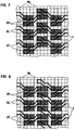
- FIG. 7 shows a layout for a dynamic memory cell arrangement with manufactured by the inventive method Storage capacitors shown.
- Word lines run perpendicular to each other WL and bit lines BL.
- the storage capacitors SP are as hatched rectangles.
- the location of the selection transistor pairs AT is a bold outline registered.
- In the layout in Figure 13 are as dash-dotted Lines T entered the separating columns of the mask with which the Layer structures 4 'or 24' in the subareas in their Shape correspond to the shape of the storage capacitors SP, be separated.
- the layer structures 4 'and 24' are in this layout arranged in columns, with adjacent columns by half the distance between the neighboring centers Layer structures 4 ', 24' arranged offset from one another are.
- the layer structures In order to achieve the highest possible packing density, it is advantageous to form the layer structures with a square cross section and a side length of 3 F, where F is the minimum structure size that can be produced in the respective technology.
- the distance between adjacent layer structures 4 ', 24' is F.
- the widths and spacings of the word lines WL and bit lines BL are also F.
- a memory cell has an area requirement of 8 F 2 .
- 12 layers of doped silicon 4 1 or 24 1 are required. With a layer thickness of the layers of doped silicon 4 1 or 24 1 and the germanium-containing layers 4 2 or 24 2 of 20 nm, this results in a stack height of approximately 0.4 ⁇ m.
- FIG. 8 shows another layout for a dynamic memory cell arrangement with one according to the inventive method manufactured storage capacitors shown.
- the word lines WL, bit lines BL, storage capacitors SP, selection transistor pairs AT are again the separation columns T shown.
- This layout differs from that in Figure 14 illustrated layout in that the layer structures 4 ', 24', from which the partial areas are separated are formed for the storage capacitors SP, in a grid are arranged. Adjacent columns are not against each other staggered. The distance from neighboring Separation columns T are twice as large in this layout as in the layout shown in Figure 13. For that it has in figure 13 layout compared to that shown in FIG Layout the advantage that a more relaxed at the resolution limit Lithography is available. This is done with finer Purchased structures in the separation mask.
- the separating gaps T are preferably located in the separating mask Formed using a so-called CARL lacquer. With these Varnishing becomes the breadth through a chemical aftertreatment the structure sizes changed so that the separation column T a smaller width than the minimum structure size that can be produced F in the respective technology.
Abstract
Zur Herstellung eines Kondensators, insbesondere für eine dyamische Speicherzellenanordnung mit Stapelkondensatoren, wird eine Schichtenfolge erzeugt, die alternierend Schichten aus dotiertem Silizium und germaniumhaltige Schichten enthält. Aus der Schichtenfolge werden Schichtstrukturen gebildet, deren Flanken jeweils mit einer leitfähigen Stützstruktur (5) versehen werden. In den Schichtstrukturen werden Öffnungen, insbesondere Spalten gebildet, in denen die Oberfläche der Schichten freiliegt. Die germaniumhaltigen Schichten werden selektiv zu den Schichten aus dotiertem Silizium entfernt. Die freiliegende Oberfläche der Schichten aus dotiertem Silizium (41) und der Stützstruktur (5) werden mit einem Kondensatordielektrikum (6) versehen, auf das eine Gegenelektrode (7) aufgebracht wird. <IMAGE> <IMAGE>In order to produce a capacitor, in particular for a dynamic memory cell arrangement with stacked capacitors, a layer sequence is generated which contains alternating layers of doped silicon and layers containing germanium. Layer structures are formed from the layer sequence, the flanks of which are each provided with a conductive support structure (5). Openings, in particular gaps, are formed in the layer structures, in which the surface of the layers is exposed. The germanium-containing layers are selectively removed from the layers of doped silicon. The exposed surface of the layers of doped silicon (41) and the support structure (5) are provided with a capacitor dielectric (6), to which a counter electrode (7) is applied. <IMAGE> <IMAGE>
Description
Für verschiedene integrierte Schaltungstypen, wie zum Beispiel dynamische Speicherzellenanordnungen, Analog Digital- und Digital Ahalog-Wandler sowie Filterschaltungen, werden Kondensatoren auf Halbleiterbasis benötigt. Bei der Herstellung von Kondensatoren auf Halbleiterbasis ist im Hinblick auf eine erhöhte Integrationsdichte oder reduzierte Chipfläche das Problem zu lösen, den Platzbedarf des Kondensators bei gleichbleibender Kapazität zu reduzieren.For various integrated circuit types, such as dynamic memory cell arrangements, analog digital and Digital Ahalog converters as well as filter circuits Semiconductor-based capacitors required. In the preparation of of capacitors based on semiconductors is in consideration to an increased integration density or reduced chip area to solve the problem of the space requirement of the capacitor to reduce with constant capacity.
Dieses Problem ist besonders gravierend bei dynamischen Halbleiterspeichern, bei denen die benötigte Fläche der im allgemeinen verwendeten Eintransistorspeicherzelle von Speichergeneration zu Speichergeneration mit zunehmender Speicherdichte reduziert wird. Gleichzeitig muß eine gewisse Mindestkapazität des Speicherkondensators erhalten bleiben.This problem is particularly serious with dynamic semiconductor memories, where the area needed is generally used single transistor memory cell from memory generation to storage generation with increasing storage density is reduced. At the same time, there must be a certain minimum capacity of the storage capacitor are retained.
Eine Eintransistorspeicherzelle einer dynamischen Halbleiterspeicheranordnung (DRAM-Speicheranordnung) umfaßt einen Auslesetransistor und einen Kondensator. In dem Kondensator ist die Information in Form einer elektrischen Ladung gespeichert, die eine logische Größe, Null oder Eins, darstellt. Durch Ansteuerung des Auslesetransistors über eine Wortleitung kann diese Information über eine Bitleitung ausgelesen werden. Zur sicheren Speicherung der Ladung und gleichzeitigen Unterscheidbarkeit der ausgelesenen Information muß der Kondensator eine Mindestkapazität aufweisen. Die untere Grenze für die Kapazität des Speicherkondensators wird derzeit bei 25 fF gesehen.A single transistor memory cell of a dynamic semiconductor memory device (DRAM memory arrangement) comprises a read transistor and a capacitor. In the condenser the information is stored in the form of an electrical charge, which is a logical quantity, zero or one. By driving the read transistor via a word line can read this information over a bit line will. For safe storage of the load and simultaneous The readable information must be distinguishable Capacitor have a minimum capacitance. The lower limit for the capacity of the storage capacitor is currently seen at 25 fF.
Bis zur 1MBit-Generation wurden sowohl der Auslesetransistor als auch der Kondensator als planare Bauelemente realisiert. Ab der 4MBit-Speichergeneration wurde eine weitere Flächenreduzierung der Speicherzelle durch eine dreidimensionale Anordnung von Auslesetransistor und Speicherkondensator erzielt. Eine Möglichkeit dafür besteht darin, den Speicherkondensator in einem Graben zu realisieren (siehe zum Beispiel K. Yamada et al, Proc. Intern. Electronic Devices and Materials IEDM 85, Seite 702 ff). Die Elektroden des Speicherkondensators sind in diesem Fall entlang der Oberfläche des Grabens angeordnet. Dadurch wird die effektive Fläche des Speicherkondensators, von der die Kapazität abhängt, gegenüber dem Platzbedarf an der Oberfläche des Substrats für den Speicherkondensator, der dem Querschnitt des Grabens entspricht, vergrößert.Up to the 1MBit generation, both the readout transistor as well as the capacitor as planar components. From the 4MBit memory generation, there was a further reduction in area the memory cell by a three-dimensional arrangement achieved by read transistor and storage capacitor. One way to do this is to use the storage capacitor to be realized in a trench (see for example K. Yamada et al, Proc. Intern. Electronic devices and materials IEDM 85, page 702 ff). The electrodes of the storage capacitor are in this case along the surface of the trench arranged. This will reduce the effective area of the storage capacitor, on which the capacity depends the space requirement on the surface of the substrate for the storage capacitor, which corresponds to the cross section of the trench, enlarged.
Eine weitere Möglichkeit, zur Vergrößerung der Speicherkapazität bei gleichbleibendem oder verringertem Platzbedarf des Speicherkondensators besteht darin, den Speicherkondensator als Stapelkondensator, den sogenannten stacked capacitor, auszuführen. Dabei wird über den Wortleitungen eine Struktur aus Polysilizium, zum Beispiel eine Kronenstruktur oder ein Zylinder, gebildet, die mit dem Substrat kontaktiert wird. Diese Polysiliziumstruktur bildet den Speicherknoten. Er wird mit Kondensatordielektrikum und Kondensatorplatte versehen. Dieses Konzept hat den Vorzug, daß es weitgehend mit einem Logikprozeß kompatibel ist. Für den Speicherkondensator wird der freie Raum oberhalb der Substratoberfläche genutzt. Dabei kann die gesamte Zellfläche von der Polysiliziumstruktur überdeckt sein, solange die Polysiliziumstrukturen zu benachbarten Speicherzellen gegeneinander isoliert sind.Another way to increase storage capacity with constant or reduced space requirement of the Storage capacitor is the storage capacitor as a stacked capacitor, the so-called stacked capacitor, to execute. A structure is created over the word lines made of polysilicon, for example a crown structure or a Cylinder formed, which is contacted with the substrate. This polysilicon structure forms the storage node. He will provided with capacitor dielectric and capacitor plate. This concept has the advantage that it is largely with one Logic process is compatible. For the storage capacitor the free space above the substrate surface is used. Here can cover the entire cell area from the polysilicon structure be covered as long as the polysilicon structures to neighboring ones Memory cells are isolated from each other.
Aus EP 0 415 530 B1 ist eine Speicherzellenanordnung mit einem Stapelkondensator als Speicherkondensator bekannt. Der Stapelkondensator umfaßt eine Polysiliziumstruktur mit mehreren, im wesentlichen parallel übereinander angeordneten Polysiliziumschichten, die über mindestens eine seitliche Stütze miteinander verbunden sind. Diese kühlrippenartig angeordneten Schichten führen zu einer deutlichen Vergrößerung der Oberfläche der Polysiliziumstruktur gegenüber der Projektion der Polysiliziumstruktur auf die Substratoberfläche. Die Polysiliziumstruktur wird durch alternierende Abscheidung von Polysiliziumschichten und selektiv dazu ätzbaren SiO2- bzw. Kohlenstoffschichten auf der Oberfläche des Substrats, Strukturierung dieser Schichten, Erzeugung von Flankenbedeckungen (Spacer aus Polysilizium) an mindestens einer Flanke der Schichtstruktur und selektives Herausätzen der SiO2- bzw. Kohlenstoffschichten gebildet. Die Polysiliziumstrukturen sind dabei arsendotiert. Anschließend wird durch thermische Oxidation Siliziumoxid als Kondensatordielektrikum gebildet, auf dem eine Zellplatte aus dotiertem Polysilizium abgeschieden wird.A memory cell arrangement with a stacked capacitor as a storage capacitor is known from EP 0 415 530 B1. The stacked capacitor comprises a polysilicon structure with a plurality of polysilicon layers arranged essentially one above the other, which are connected to one another via at least one lateral support. These layers arranged in the form of a cooling fin lead to a significant increase in the surface of the polysilicon structure compared to the projection of the polysilicon structure onto the substrate surface. The polysilicon structure is formed by alternating deposition of polysilicon layers and selectively etchable SiO 2 or carbon layers on the surface of the substrate, structuring of these layers, generation of flank coverings (spacers made of polysilicon) on at least one flank of the layer structure and selective etching out of the SiO 2 or Carbon layers formed. The polysilicon structures are arsenic-doped. Subsequently, silicon oxide is formed as a capacitor dielectric by thermal oxidation, on which a cell plate made of doped polysilicon is deposited.
Aus GB 2 285 338 A ist ein Verfahren zur Herstellung eines
Kondensators bekannt, bei dem auf ein Substrat abwechselnd
Schichten aus dotiertem und undotiertem Silizium aufgebracht
werden. Durch die Schichten hindurch wird ein Kontaktloch geöffnet,
das bis in ein darunterliegendes Substrat reicht. Die
gesamte Oberfläche wird mit einer undotierten Siliziumschicht
bedeckt. Nach Strukturierung der Schichtenfolge liegen die
Flanken der Schichten aus dotiertem bzw. undotiertem Silizium
frei. Die dotierten Siliziumschichten werden selektiv zu den
undotierten Siliziumschichten entfernt. Die dabei entstehende
Siliziumstruktur wird durch Diffusion dotiert und als Elektrode
des Kondensators verwendet.
Der Erfindung liegt das Problem zugrunde, ein Verfahren zur Herstellung eines Kondensators für eine Halbleiteranordnung, insbesondere für eine DRAM-Anordnung anzugeben, bei dem gegenüber den bekannten Lösungen der Prozeßaufwand reduziert wird. Insbesondere soll der Kondensator mindestens in der für die 1 GBit-Generation erforderlichen Packungsdichte herstellbar sein.The invention is based on the problem of a method for Manufacture of a capacitor for a semiconductor device, Specify in particular for a DRAM arrangement in which the known solutions reduced the process effort becomes. In particular, the capacitor should at least in the the 1 GBit generation required packing density can be produced be.
Dieses Problem wird erfindungsgemäß gelöst durch ein Verfahren
gemäß Anspruch 1. Weitere Ausgestaltungen der Erfindung
gehen aus den übrigen Ansprüchen hervor. According to the invention, this problem is solved by a method
according to
In dem erfindungsgemäßen Verfahren wird auf einem Substrat eine Schichtenfolge erzeugt, die jeweils alternierend eine Schicht aus dotiertem Silizium und eine germaniumhaltige Schicht aufweist. Die Schichtfolge wird so strukturiert, daß mindestens eine Schichtstruktur mit bis auf das Substrat reichenden Flanken entsteht. Es wird eine Stützstruktur aus leitfähigem Material gebildet, die mindestens die Flanken der Schichtstruktur bedeckt. Die Stützstruktur wird durch selektive Epitaxie von Silizium gebildet. Vorzugsweise wird die Stützstruktur in situ dotiert. In der Schichtstruktur wird anschließend mindestens eine Öffnung gebildet, in der die Oberfläche der Schichten aus dotiertem Silizium und der germaniumhaltigen Schichten freiliegt. Anschließend werden die germaniumhaltigen Schichten selektiv zu den Schichten aus dotiertem Silizium und der Stützstruktur entfernt. Die freiliegende Oberfläche der Schichten aus dotiertem Silizium und der Stützstruktur wird mit einem Kondensatordielektrikum versehen. An der Oberfläche des Kondensatordielektrikums wird eine Gegenelektrode gebildet.In the method according to the invention is on a substrate creates a layer sequence, alternating one Layer of doped silicon and a germanium-containing Layer. The layer sequence is structured in such a way that at least one layer structure with reaching down to the substrate Flanks arises. It becomes a support structure conductive material formed at least the flanks of the Layered structure covered. The support structure is made by selective Epitaxy formed by silicon. Preferably the Support structure endowed in situ. In the layer structure then at least one opening is formed in which the Surface of the layers of doped silicon and the germanium-containing Layers exposed. Then the layers containing germanium selective to the layers of doped Silicon and the support structure removed. The exposed one Surface of the layers of doped silicon and the Support structure is provided with a capacitor dielectric. On the surface of the capacitor dielectric is a Counter electrode formed.
Die Stützstruktur ist beim Herausätzen der germaniumhaltigen Schichten vorzugsweise an mindestens drei Flanken der Schichtstruktur angeordnet. Dadurch wird eine hohe mechanische Stabilität gewährleistet, durch die ein Zusammenkleben der Schichten aus dotiertem Silizium beim Herausätzen der germaniumhaltigen Schichten aus dem zweiten Material vermieden wird. Da diese mechanische Stabilität durch die Stützstruktur gewährleistet ist, kann die Schichtdicke der Schichten aus dotiertem Silizium unabhängig von mechanischen Stabilitätsanforderungen an die Schichten aus dotiertem Silizium gewählt werden. Die Schichten aus dotiertem Silizium können insbesondere im Dickenbereich zwischen 20 und 50 nm realisiert werden. Dadurch wird auch die Gesamthöhe des Kondensators bei gleichbleibender Kapazität reduziert. The support structure is when etching out the germanium-containing Layers preferably on at least three flanks of the Layer structure arranged. This creates a high mechanical Stability guaranteed by sticking together the layers of doped silicon when etching out the layers of germanium from the second material avoided becomes. Because this mechanical stability through the support structure is guaranteed, the layer thickness of the layers made of doped silicon regardless of mechanical stability requirements to the layers of doped silicon to get voted. The layers of doped silicon can realized in particular in the thickness range between 20 and 50 nm will. This will also increase the total height of the capacitor reduced with the same capacity.
Die Schichten aus dotiertem Silizium können sowohl polykristallin als auch kristallin oder amorph sein.The layers of doped silicon can be both polycrystalline as well as being crystalline or amorphous.
Es liegt im Rahmen der Erfindung, die germaniumhaltigen Schichten aus reinem Germanium oder aus Silizium und Germanium zu bilden. Werden die Schichten aus Silizium und Germanium gebildet, so liegt der Germaniumanteil vorzugsweise zwischen 10 Prozent und 100 Prozent. Der Siliziumanteil liegt zwischen 0 Prozent und 90 Prozent. Die germaniumhaltigen Schichten können sowohl dotiert als auch undotiert abgeschieden werden.It is within the scope of the invention to contain the germanium Layers of pure germanium or of silicon and germanium to build. The layers are made of silicon and germanium formed, the germanium content is preferably between 10 percent and 100 percent. The silicon content is between 0 percent and 90 percent. The layers containing germanium can be deposited both doped and undoped.
Germaniumhaltige Schichten aus reinem Germanium oder aus Silizium und Germanium lassen sich naßchemisch mit guter Selektivität zu Silizium ätzen. Bei Verwendung einer Ätzmischung, die HF, H2O2 und CH3COOH enthält, beträgt die Selektivität der Ätzung zu Silizium 1:30 bis 1:1000. Bei dieser Ätzung beträgt die Selektivität zu Siliziumoxid und Siliziumnitrid etwa 1:30 bis 1:1000.Germanium-containing layers of pure germanium or of silicon and germanium can be etched wet-chemically with good selectivity to silicon. If an etching mixture containing HF, H 2 O 2 and CH 3 COOH is used, the selectivity of the etching to silicon is 1:30 to 1: 1000. With this etching, the selectivity to silicon oxide and silicon nitride is approximately 1:30 to 1: 1000.
Mit Cholin lassen sich Siliziumschichten selektiv zu Germanium ätzen.With choline, silicon layers can be selectively converted to germanium etching.
Da die Diffusionskoeffizienten von Germanium in Silizium und von Silizium in Germanium äußerst gering sind, bleibt die Schichtenfolge auch bei prozeßbedingten Temperaturbelastungen von zum Beispiel 800°C unverändert erhalten. Die Diffusionskoeffizienten liegen bei einer Prozeßtemperatur von 1000°C etwa bei 1,5 x 10⁻⁶ cm2/sec. Zum Vergleich: diese Diffusionskoeffizienten sind damit etwa um einen Faktor 10 geringer als der Diffusionskoeffizient von Bor in Silizium.Since the diffusion coefficients of germanium in silicon and of silicon in germanium are extremely low, the layer sequence remains unchanged even at process-related temperature loads of, for example, 800 ° C. The diffusion coefficients at a process temperature of 1000 ° C are approximately 1.5 x 10 -6 cm 2 / sec. For comparison: these diffusion coefficients are about 10 times lower than the diffusion coefficient of boron in silicon.
Vorzugsweise werden die Schichten aus dotiertem Silizium in einem CVD-Prozeß unter Verwendung von Silan als Prozeßgas im Temperaturbereich zwischen 400 und 600°C bei einem Druck zwischen 10 und 400 Torr und einem Silanfluß von 30 bis 300 sccm mit Abscheideraten von 10 bis 100 nm pro Minute gebildet. Die germaniumhaltigen Schichten werden vorzugsweise durch CVD-Abscheidung unter Verwendung von German bzw. German und Disilan im Prozeßgas bei einer Temperatur zwischen 400 und 600°C und einem Druck zwischen 10 und 400 Torr gebildet, wobei der Germanfluß und gegebenenfalls der Disilanfluß zwischen 30 und 300 sccm eingestellt wird und die Abscheiderate zwischen 10 und 100 nm pro Minute liegt.The layers are preferably made of doped silicon a CVD process using silane as process gas in the Temperature range between 400 and 600 ° C at a pressure between 10 and 400 torr and a silane flow of 30 to 300 sccm with deposition rates of 10 to 100 nm per minute. The Germanium-containing layers are preferably by CVD deposition using German or German and Disilan in the process gas at a temperature between 400 and 600 ° C and a pressure between 10 and 400 Torr, the German river and possibly the disilane flow between 30 and 300 sccm is set and the deposition rate between 10 and is 100 nm per minute.
Die dotierten Siliziumschichten werden vorzugsweise in situ dotiert abgeschieden. Dazu wird der Abscheidung ein Dotiergas, zum Beispiel Arsin, Phosphin oder Diboran. Die Schichten aus dotiertem Silizium und die Stützstruktur können sowohl aus n-dotiertem als auch aus p-dotiertem Silizium gebildet werden.The doped silicon layers are preferably in situ endowed deposited. For this, the deposition becomes a doping gas, for example arsine, phosphine or diborane. The layers made of doped silicon and the support structure can both formed from n-doped as well as from p-doped silicon will.
Dotiertes Silizium und Germanium können in demselben Reaktor abgeschieden werden. Dadurch kann die Schichtenfolge ohne Anlagenwechsel nur durch Umschalten der Prozeßparameter realisiert werden. Dieses bedeutet eine deutliche Prozeßvereinfachung.Doped silicon and germanium can be in the same reactor be deposited. This enables the layer sequence to be changed without changing the system only realized by switching the process parameters will. This means a significant process simplification.
In Anwendungen, in denen die Stützstruktur und die Schichten aus dotiertem Silizium mit dem Substrat elektrisch verbunden werden sollen, ist es vorteilhaft, die Dotierung der Stützstruktur und der Schichten aus dotiertem Silizium entsprechend der Dotierung des Substrates im Bereich der Stützstruktur zu wählen, um die Bildung eines pn-Übergangs zu vermeiden.In applications where the support structure and the layers made of doped silicon electrically connected to the substrate , it is advantageous to dope the support structure and the layers of doped silicon accordingly the doping of the substrate in the area of the support structure to avoid the formation of a pn junction.
Die Stützstruktur wird mit definierten Oberflächen an den Flanken der Schichtstruktur gebildet. Dadurch wird sichergestellt, daß die germaniumhaltigen Schichten gleichmäßig zwischen den Schichten aus dotiertem Silizium herausgeätzt werden. Auf diese Weise wird verhindert, daß die germaniumhaltigen Schichten lokal noch nicht herausgeätzt sind und gleichzeitig an anderen Stellen die Stützflächen schon so stark angegriffen werden, daß einzelne Schichten aus dotiertem Silizium herunterfallen. The support structure is provided with defined surfaces on the Flanks of the layer structure are formed. This ensures that the germanium-containing layers evenly between the layers of doped silicon are etched out. This prevents the germanium-containing Layers are not yet etched out locally and at the same time in other places the supporting surfaces were already so badly attacked that individual layers of doped silicon falling off.
Vorzugsweise werden bei der Bildung der Öffnung in der Schichtstruktur die Schichtstruktur und die Stützstruktur in zwei Teilbereiche geteilt, die durch einen bis auf die Oberfläche des Substrats reichenden Spalt beabstandet sind. Aus den beiden Teilbereichen werden zwei Kondensatoren gebildet. Der Abstand und die Strukturgröße der Teilbereiche können dabei jeweils entsprechend der minimalen Strukturgröße F in der jeweiligen Technologie gebildet werden. Dadurch wird eine hohe Packungsdichte erzielt.Preferably, when forming the opening in the Layer structure the layer structure and the support structure in divided into two sections by one down to the surface of the substrate-extending gap are spaced. Out Two capacitors are formed in the two sections. The distance and the structure size of the sub-areas can each corresponding to the minimum structure size F in the respective technology. This makes a high one Packing density achieved.
Bei Herstellung des Kondensators als Speicherkondensator für eine dynamische Speicherzellenanordnung erfolgt die Herstellung des Kondensators vorzugsweise als Stapelkondensator. In diesem Fall umfaßt das Substrat ein Halbleitersubstrat mit Auswahltransistoren, Bitleitungen, Wortleitungen und einer isolierenden Schicht, auf deren Oberfläche die Schichtenfolge aufgebracht wird. Vorzugsweise wird die isolierende Schicht planarisiert, so daß die Schichtenfolge auf einer im wesentlichen planaren Oberfläche gebildet wird.When manufacturing the capacitor as a storage capacitor for A dynamic memory cell arrangement is used to manufacture the device of the capacitor preferably as a stacked capacitor. In In this case, the substrate also includes a semiconductor substrate Selection transistors, bit lines, word lines and one insulating layer, on the surface of which the layer sequence is applied. Preferably the insulating layer planarized so that the layer sequence is essentially on one planar surface is formed.
Im folgenden wird die Erfindung anhand der Figuren und der Ausführungsbeispiele näher erläutert.
Figur 1- zeigt ein Substrat mit einer Schichtenfolge, die alternierend Schichten aus dotiertem Silizium und germaniumhaltige Schichten aufweist.
Figur 2- zeigt das Substrat mit Schichtstrukturen.
Figur 3- zeigt das Substrat nach Bildung einer Stützstruktur, die die Flanken der Schichtstruktur bedeckt.
Figur 4- zeigt das Substrat nach Bildung einer Öffnung in den Schichtstrukturen und selektivem Herausätzen von germaniumhaltigen Schichten.
Figur 5- zeigt das Substrat nach Bildung eines Kondensatordielektrikums und einer Gegenelektrode.
Figur 6- zeigt den in
Figur 5 mit VI-VI bezeichneten Schnitt durch das Substrat. Figur 7- zeigt ein Layout, bei dem die Schichtstrukturen versetzt angeordnet sind.
Figur 8- zeigt ein Layout, bei dem die Schichtstrukturen rasterförmig angeordnet sind.
- Figure 1
- shows a substrate with a layer sequence which has alternating layers of doped silicon and germanium-containing layers.
- Figure 2
- shows the substrate with layer structures.
- Figure 3
- shows the substrate after the formation of a support structure which covers the flanks of the layer structure.
- Figure 4
- shows the substrate after formation of an opening in the layer structures and selective etching out of germanium-containing layers.
- Figure 5
- shows the substrate after formation of a capacitor dielectric and a counter electrode.
- Figure 6
- shows the section designated VI-VI in FIG. 5 through the substrate.
- Figure 7
- shows a layout in which the layer structures are arranged offset.
- Figure 8
- shows a layout in which the layer structures are arranged in a grid.
Auf ein Substrat 1 wird eine isolierende Schicht 2 aufgebracht.
Das Substrat 1 ist zum Beispiel ein Halbleitersubstrat,
insbesondere eine monokristalline Siliziumscheibe,
das Auswahltransistoren mit Wortleitungen und Bitleitungen
umfaßt. Die isolierende Schicht wird zum Beispiel aus SiO2
gebildet und mit Hilfe von Planarisierungsverfahren planarisiert
(siehe Figur 1). In der isolierenden Schicht 2 werden
Kontaktlöcher 3 geöffnet und mit elektrisch leitfähigem Material,
zum Beispiel dotiertes Polysilizium, Wolfram, Tantal,
Titan, Titannitrid oder Wolframsilizid aufgefüllt. Die Kontaktlöcher
3 werden so angeordnet, daß sie jeweils auf ein
Source/Drain-Gebiet eines der Auswahltransistoren im Substrat
1 reichen.An insulating
Auf die Oberfläche der isolierenden Schicht 2 wird eine
Schichtenfolge 4 aufgebracht, die jeweils alternierend
Schichten aus dotiertem Silizium 41 und germaniumhaltige
Schichten 42 umfaßt. Die Schichten aus dotiertem Silizium 41
können sowohl p+- als auch n+-dotiert sein und weisen eine
Dotierstoffkonzentration von zum Beispiel 5 x 1020 cm-3 auf.
Die Schichten aus dotiertem Silizium 41 und die germaniumhaltigen
Schichten 42 werden in einer Schichtdicke von jeweils
20 nm zum Beispiel durch CVD-Abscheidung unter Verwendung von
Silan bzw. German oder German und Disilan bei einer Temperatur
zwischen 400°C und 600°C und einem Druck zwischen 10 und
400 Torr abgeschieden. Der Gasfluß liegt dabei jeweils zwischen
30 und 300 sccm, die Abscheiderate liegt zwischen 10
und 100 nm/min. Die oberste Schicht der Schichtenfolge ist
eine germaniumhaltige Schicht 42.A
Anschließend werden aus der Schichtenfolge 4 durch anisotropes
Ätzen unter Verwendung einer Maske Schichtstrukturen 4'
gebildet. Zwischen den Schichtstrukturen 4' liegt die Oberfläche
der isolierenden Schicht 2 frei (siehe Figur 2). Das
anisotrope Ätzen erfolgt zum Beispiel mit CF4 und SF6.
Anschließend wird mittels selektiver Epitaxie von Silizium
eine Stützstruktur 5 gebildet (siehe Figur 3). Die selektive
Epitaxie wird in einem Prozeß unter Verwendung von SiCl2H2,
Hcl, H2 und einem Dotiergas, zum Beispiel B2H6 oder PH3 als
Prozeßgas im Temperaturbereich zwischen 700°C und 900°C
durchgeführt. Bei der selektiven Epitaxie wächst die Stützstruktur
5 in situ dotiert auf der Oberfläche der Schichtstrukturen
4' auf. Auf der Oberfläche der isolierenden
Schicht 2 wächst dagegen kein Silizium auf. Die Stützstruktur
5 bedeckt die Flanken und die Oberfläche der Schichtstrukturen
4' vollständig.A
Anschließend werden die Schichtstrukturen 4' mit der sie bedeckenden
Stützstruktur 5 unter Verwendung einer photolithographisch
erzeugten Maske durch anisotropes Ätzen zum Beispiel
mit CF4 und SF6 so strukturiert, daß jeweils zwei Teilbereiche
entstehen. Die beiden Teilbereiche sind jeweils
durch einen Spalt voneinander getrennt. Im Bereich des Spaltes
weisen die Teilbereiche jeweils eine Flanke auf, an der
die Oberfläche der germaniumhaltigen Schichten 42 und der
Schichten aus dotiertem Silizium 41 freiliegt.Subsequently, the layer structures 4 'with the
Durch eine zu dotiertem Polysilizium und SiO2 selektive Ätzung
werden anschließend die verbleibenden Teile der germaniumhaltigen
Schichten 42 entfernt. Die selektive Ätzung erfolgt
zum Beispiel naßchemisch mit einer Ätzmischung, die HF,
H2O2 und CH3COOH enthält. Vorzugsweise liegt die Konzentration
der Lösung in folgendem Bereich: 1 Teil HF, 200 Teile
H2O2, 300 Teile CH3COOH. Diese Ätzung weist in Bezug auf dotiertes
Polysilizium eine Selektivität von 1:30 bis 1:1000
auf. In Bezug auf Siliziumoxid und Siliziumnitrid weist sie
eine Selektivität von 1:30 bis 1:1000 auf.The remaining parts of the germanium-containing
Die Schichten aus dotiertem Silizium 41 und die Stützstruktur
5, die von der selektiven Ätzung nicht angegriffen werden,
sind mechanisch und elektrisch miteinander verbunden.The layers of doped
Die Oberfläche der Schichten aus dotiertem Silizium 41 und
der Stützstruktur 5 wird mit einem Kondensatordielektrikum 6
versehen. Das Kondensatordielektrikum 6 wird zum Beispiel aus
einer Dreifachschicht aus SiO2, Si3N4 und SiO2 in einer
oxidäquivalenten Dicke von 4 nm gebildet.The surface of the layers of doped
Durch Abscheidung einer in situ dotierten Polysiliziumschicht
wird anschließend eine Gegenelektrode 7 gebildet (siehe Figur
5 und Figur 6). Die Gegenelektrode 7 ist zum Beispiel n+-dotiert
mit einer Dotierstoffkonzentrtion im Bereich von 5 x
1020 cm-3.A
In dem in Figur 6 dargestellten Schnitt sind im Substrat 1
Auswahltransistoren angedeutet. Die Schichten aus dotiertem
Silizium 41 und die damit verbundene Stützstruktur 5 bilden
jeweils einen Speicherknoten für einen Speicherkondensator.
Dieser Speicherknoten ist über den darunter angeordneten Kontakt
3 mit einem Source/Drain-Gebiet 8 eines Auswahltransistors
verbunden. Das andere Source/Drain-Gebiet 9 des Auswahltransistors
ist über ein Anschlußgebiet 10 mit dem entsprechenden
Source/Drain-Gebiet 9 des benachbarten Auswahltransistors
verbunden. Das Anschlußgebiet 10 ist ferner über
einen vergrabenen Bitleitungskontakt 11 mit einer vergrabenen
Bitleitung 12 verbunden. Die vergrabene Bitleitung 12 und der
Bitleitungskontakt 11 sind durch die isolierende Schicht 2
umgeben. Zwischen den Source/Drain-Gebieten 8 und 9 eines
Auswahltransistors sind das Kanalgebiet 13, ein Gatedielektrikum
(nicht dargestellt) und eine als Wortleitung 14 wirkende
Gateelektrode angeordnet. Die Wortleitung 14 und der
Bitleitungskontakt 11 sind jeweils aus dotiertem Polysilizium
gebildet. Die Bitleitung 12 wird aus dotiertem Polysilizium,
Wolframsilizid oder Wolfram gebildet. Auf der der Bitleitung
12 abgewandten Seite des Source/Drain-Gebietes 8 ist jeweils
eine Isolationsstruktur, zum Beispiel ein flacher, mit isolierendem
Material gefüllter Graben 15 (Shallow trench isolation)
zur Isolation zwischen benachbarten Auswahltransistorpaaren
vorgesehen.In the section shown in FIG. 6, selection transistors are indicated in the
In Figur 7 ist ein Layout für eine dynamische Speicherzellenanordnung mit nach dem erfindungsgemäßen Verfahren hergestellten Speicherkondensatoren dargestellt. In der Speicherzellenanordnung verlaufen senkrecht zueinander Wortleitungen WL und Bitleitungen BL. Die Speicherkondensatoren SP sind als schraffierte Rechtecke eingezeichnet. Die Lage der Auswahltransistorpaare AT ist jeweils als fettgestrichelte Konturlinie eingetragen. Bei der Herstellung werden jeweils zwei Speicherkondensatoren aus einer Schichtstruktur 4' bzw. 24' gebildet. In dem Layout in Figur 13 sind als strichpunktierte Linien T die Trennspalten der Maske eingetragen, mit der die Schichtstrukturen 4' bzw. 24' in die Teilbereiche, die in ihrer Form der Form der Speicherkondensatoren SP entsprechen, aufgetrennt werden. Die Schichtstrukturen 4' bzw. 24' sind in diesem Layout in Spalten angeordnet, wobei benachbarte Spalten um den halben Abstand zwischen den Mittelpunkten benachbarten Schichtstrukturen 4', 24' gegeneinander versetzt angeordnet sind.FIG. 7 shows a layout for a dynamic memory cell arrangement with manufactured by the inventive method Storage capacitors shown. In the memory cell arrangement Word lines run perpendicular to each other WL and bit lines BL. The storage capacitors SP are as hatched rectangles. The location of the selection transistor pairs AT is a bold outline registered. During the manufacturing process, two Storage capacitors made of a layer structure 4 'or 24' educated. In the layout in Figure 13 are as dash-dotted Lines T entered the separating columns of the mask with which the Layer structures 4 'or 24' in the subareas in their Shape correspond to the shape of the storage capacitors SP, be separated. The layer structures 4 'and 24' are in this layout arranged in columns, with adjacent columns by half the distance between the neighboring centers Layer structures 4 ', 24' arranged offset from one another are.
Zur Erzielung einer möglichst hohen Packungsdichte ist es
vorteilhaft, die Schichtstrukturen mit quadratischem Querschnitt
und einer Seitenlänge von 3 F, wobei F die in der jeweiligen
Technologie minimale herstellbare Strukturgröße ist,
zu bilden. Der Abstand zwischen benachbarten Schichtstrukturen
4', 24' beträgt F. Dann betragen auch die Breiten und Abstände
der Wortleitungen WL und Bitleitungen BL jeweils F.
Eine Speicherzelle hat in diesem Fall einen Flächenbedarf von
8 F2. Um bei einer Strukturgröße F von 0,18 µm, wie sie in
der 1GBit-Generation vorgesehen ist, die für die dynamische
Speicherzellenanordnung erforderliche Mindestkapazität von 25
fF zu erzielen, sind 12 Schichten aus dotiertem Silizium 41
bzw. 241 erforderlich. Bei einer Schichtdicke der Schichten
aus dotiertem Silizium 41 bzw. 241 und der germaniumhaltigen
Schichten 42 bzw. 242 von 20 nm ergibt sich dabei eine Stapelhöhe
von etwa 0,4 µm.In order to achieve the highest possible packing density, it is advantageous to form the layer structures with a square cross section and a side length of 3 F, where F is the minimum structure size that can be produced in the respective technology. The distance between adjacent layer structures 4 ', 24' is F. Then the widths and spacings of the word lines WL and bit lines BL are also F. In this case, a memory cell has an area requirement of 8 F 2 . In order to achieve the minimum capacitance of 25 fF required for the dynamic memory cell arrangement with a structure size F of 0.18 μm, as is provided in the 1 GBit generation, 12 layers of doped
In Figur 8 ist ein weiteres Layout für eine dynamische Speicherzellenanordnung mit einem nach dem erfindungsgemäßen Verfahren hergestellten Speicherkondensatoren dargestellt. Neben den Wortleitungen WL, Bitleitungen BL, Speicherkondensatoren SP, Auswahltransistorpaaren AT sind wiederum die Trennspalten T dargestellt. Dieses Layout unterscheidet sich von dem in Figur 14 dargestellten Layout dadurch, daß die Schichtstrukturen 4', 24', aus denen durch Auftrennen die Teilbereiche für die Speicherkondensatoren SP gebildet werden, rasterförmig angeordnet sind. Benachbarte Spalten sind dabei nicht gegeneinander versetzt angeordnet. Der Abstand benachbarter Trennspalten T ist in diesem Layout doppelt so groß als in dem in Figur 13 dargestellten Layout. Dafür hat das in Figur 13 dargestellte Layout gegenüber dem in Figur 14 dargestellten Layout den Vorteil, daß an der Auflösungsgrenze eine entspanntere Lithographie vorliegt. Dieses wird mit feineren Strukturen in der Trennmaske erkauft.FIG. 8 shows another layout for a dynamic memory cell arrangement with one according to the inventive method manufactured storage capacitors shown. Next the word lines WL, bit lines BL, storage capacitors SP, selection transistor pairs AT are again the separation columns T shown. This layout differs from that in Figure 14 illustrated layout in that the layer structures 4 ', 24', from which the partial areas are separated are formed for the storage capacitors SP, in a grid are arranged. Adjacent columns are not against each other staggered. The distance from neighboring Separation columns T are twice as large in this layout as in the layout shown in Figure 13. For that it has in figure 13 layout compared to that shown in FIG Layout the advantage that a more relaxed at the resolution limit Lithography is available. This is done with finer Purchased structures in the separation mask.
Vorzugsweise werden die Trennspalten T in der Trennmaske unter Verwendung eines sogenannten CARL-Lack gebildet. Bei diesen Lacken wird durch eine chemische Nachbehandlung die Breite der Strukturgrößen verändert, so daß die Trennspalte T eine geringere Weite als die minimal herstellbare Strukturgröße F in der jeweiligen Technologie aufweisen. The separating gaps T are preferably located in the separating mask Formed using a so-called CARL lacquer. With these Varnishing becomes the breadth through a chemical aftertreatment the structure sizes changed so that the separation column T a smaller width than the minimum structure size that can be produced F in the respective technology.
- 1, 211, 21
- SubstratSubstrate
- 2, 222, 22
- isolierende Schichtinsulating layer
- 3, 233, 23
- KontaktlöcherContact holes
- 4, 244, 24
- SchichtenfolgeLayer sequence
- 4', 24'4 ', 24'
- SchichtstrukturLayer structure
- 41, 241 4 1 , 24 1
- Schichten aus dotiertem SiliziumDoped silicon layers
- 42, 242 4 2 , 24 2
- germaniumhaltige Schichtenlayers containing germanium
- 5, 25'5, 25 '
- StützstrukturSupport structure
- 2525th
- polykristalline Siliziumschichtpolycrystalline silicon layer
- 6, 266, 26
- KondensatordielektrikumCapacitor dielectric
- 7, 277, 27
- GegenelektrodeCounter electrode
- 8, 98, 9
- Source/Drain-GebieteSource / drain areas
- 1010th
- AnschlußgebietService area
- 1111
- BitleitungskontaktBit line contact
- 1212th
- BitleitungBit line
- 1313
- KanalgebietCanal area
- 1414
- WortleitungWord line
- 1515
- IsolationsstrukturIsolation structure
- WLWL
- WortleitungWord line
- BLBL
- BitleitungBit line
- SPSP
- SpeicherkondensatorStorage capacitor
- ATAT
- AuswahltransistorpaarSelection transistor pair
- TT
- TrennspalteSeparation column
Claims (6)
bei dem die selektive Epitaxie unter Verwendung von SiCl2H2, HCl, H2 und einem Dotiergas durchgeführt wird.The method of claim 1 or 2,
in which the selective epitaxy is carried out using SiCl 2 H 2 , HCl, H 2 and a doping gas.
bei dem bei der Bildung der Öffnung in der Schichtstruktur (4') die Schichtstruktur mit der Stützstruktur (5) in zwei Teilbereiche geteilt wird, die durch einen Spalt beabstandet sind.Method according to one of claims 1 to 3,
in which, when the opening is formed in the layer structure (4 '), the layer structure with the support structure (5) is divided into two partial regions which are spaced apart by a gap.
bei dem die germaniumhaltigen Schichten (42, 242) einen Germaniumanteil zwischen 10 und 100 Mol% und einen Siliziumanteil zwischen 0 und 90 Mol% aufweisen.Method according to one of claims 1 to 4,
in which the germanium-containing layers (4 2 , 24 2 ) have a germanium content between 10 and 100 mol% and a silicon content between 0 and 90 mol%.
bei dem das Substrat (1) ein Halbleitersubstrat mit Auswahltransistoren (AT), Bitleitungen (BL), Wortleitungen (WL) und einer isolierenden Schicht (2) umfaßt, auf deren Oberfläche die Schichtenfolge (4) aufgebracht wird.Method according to one of claims 1 to 5,
in which the substrate (1) comprises a semiconductor substrate with selection transistors (AT), bit lines (BL), word lines (WL) and an insulating layer (2), on the surface of which the layer sequence (4) is applied.
Applications Claiming Priority (2)
| Application Number | Priority Date | Filing Date | Title |
|---|---|---|---|
| DE19707977 | 1997-02-27 | ||
| DE19707977A DE19707977C1 (en) | 1997-02-27 | 1997-02-27 | Capacitor production especially for DRAM cell array |
Publications (1)
| Publication Number | Publication Date |
|---|---|
| EP0862204A1 true EP0862204A1 (en) | 1998-09-02 |
Family
ID=7821730
Family Applications (1)
| Application Number | Title | Priority Date | Filing Date |
|---|---|---|---|
| EP98101832A Withdrawn EP0862204A1 (en) | 1997-02-27 | 1998-02-03 | Method for fabricating a capacitor for a semiconductor structure |
Country Status (5)
| Country | Link |
|---|---|
| EP (1) | EP0862204A1 (en) |
| JP (1) | JPH10242430A (en) |
| KR (1) | KR19980071494A (en) |
| DE (1) | DE19707977C1 (en) |
| TW (1) | TW421888B (en) |
Families Citing this family (9)
| Publication number | Priority date | Publication date | Assignee | Title |
|---|---|---|---|---|
| DE19821910C1 (en) * | 1997-02-27 | 1999-11-11 | Siemens Ag | Stacked capacitor manufacturing method |
| DE19842704C2 (en) * | 1998-09-17 | 2002-03-28 | Infineon Technologies Ag | Manufacturing process for a capacitor with a high epsilon dielectric or a ferroelectric according to the fin stack principle using a negative mold |
| DE19842682A1 (en) * | 1998-09-17 | 2000-04-06 | Siemens Ag | Capacitor with a high-e dielectric or a ferro-electrical according to the fin stack principle and manufacturing process |
| KR100567049B1 (en) * | 1999-10-26 | 2006-04-04 | 주식회사 하이닉스반도체 | Isolation forming method for semiconductor device |
| FR2800913B1 (en) * | 1999-11-10 | 2004-09-03 | St Microelectronics Sa | METHOD FOR MANUFACTURING A CAPACITY STACK, PARTICULARLY FOR DYNAMIC DIRECT ACCESS MEMORIES |
| KR100442779B1 (en) * | 2001-12-20 | 2004-08-04 | 동부전자 주식회사 | Method for manufacturing dram device |
| KR100487558B1 (en) * | 2003-03-03 | 2005-05-03 | 삼성전자주식회사 | Ferroelectric memory device equipped with semi-cylindrical capacitor and method for thereof |
| TWI233689B (en) * | 2003-04-14 | 2005-06-01 | Samsung Electronics Co Ltd | Capacitors of semiconductor devices including silicon-germanium and metallic electrodes and methods of fabricating the same |
| KR102473658B1 (en) | 2016-05-27 | 2022-12-02 | 삼성전자주식회사 | Semiconductor device |
Citations (5)
| Publication number | Priority date | Publication date | Assignee | Title |
|---|---|---|---|---|
| US5155657A (en) * | 1991-10-31 | 1992-10-13 | International Business Machines Corporation | High area capacitor formation using material dependent etching |
| DE4229363A1 (en) * | 1991-09-06 | 1993-03-11 | Micron Technology Inc | METHOD FOR FORMING A CONDENSER |
| US5405801A (en) * | 1992-02-28 | 1995-04-11 | Samsung Electronics Co., Ltd. | Method for manufacturing a capacitor of a semiconductor device |
| GB2285338A (en) * | 1993-12-29 | 1995-07-05 | Hyundai Electronics Ind | Method for fabricating capacitor |
| US5455204A (en) * | 1994-12-12 | 1995-10-03 | International Business Machines Corporation | Thin capacitor dielectric by rapid thermal processing |
Family Cites Families (1)
| Publication number | Priority date | Publication date | Assignee | Title |
|---|---|---|---|---|
| JPH0338061A (en) * | 1989-07-05 | 1991-02-19 | Fujitsu Ltd | Semiconductor memory |
-
1997
- 1997-02-27 DE DE19707977A patent/DE19707977C1/en not_active Expired - Fee Related
-
1998
- 1998-01-20 TW TW087100726A patent/TW421888B/en not_active IP Right Cessation
- 1998-02-03 EP EP98101832A patent/EP0862204A1/en not_active Withdrawn
- 1998-02-19 KR KR1019980005088A patent/KR19980071494A/en not_active Application Discontinuation
- 1998-02-25 JP JP10059129A patent/JPH10242430A/en not_active Withdrawn
Patent Citations (5)
| Publication number | Priority date | Publication date | Assignee | Title |
|---|---|---|---|---|
| DE4229363A1 (en) * | 1991-09-06 | 1993-03-11 | Micron Technology Inc | METHOD FOR FORMING A CONDENSER |
| US5155657A (en) * | 1991-10-31 | 1992-10-13 | International Business Machines Corporation | High area capacitor formation using material dependent etching |
| US5405801A (en) * | 1992-02-28 | 1995-04-11 | Samsung Electronics Co., Ltd. | Method for manufacturing a capacitor of a semiconductor device |
| GB2285338A (en) * | 1993-12-29 | 1995-07-05 | Hyundai Electronics Ind | Method for fabricating capacitor |
| US5455204A (en) * | 1994-12-12 | 1995-10-03 | International Business Machines Corporation | Thin capacitor dielectric by rapid thermal processing |
Also Published As
| Publication number | Publication date |
|---|---|
| TW421888B (en) | 2001-02-11 |
| KR19980071494A (en) | 1998-10-26 |
| JPH10242430A (en) | 1998-09-11 |
| DE19707977C1 (en) | 1998-06-10 |
Similar Documents
| Publication | Publication Date | Title |
|---|---|---|
| EP0744771B1 (en) | Method of making a DRAM storage cell with a vertical transistor | |
| EP0744772B1 (en) | DRAM storage cell with vertical transistor and method for production thereof | |
| DE3841588C2 (en) | ||
| DE19941148B4 (en) | Trench capacitor and select transistor memory and method of making the same | |
| DE19546999C1 (en) | Capacitor mfg system for semiconductor device | |
| EP0875937A2 (en) | DRAM cell array and method of making the same | |
| DE10228717B4 (en) | A method for isolating active areas of semiconductor memory elements and for insulating element areas of a semiconductor wafer | |
| EP1116270A1 (en) | Integrated circuit comprising vertical transistors, and a method for the production thereof | |
| DE19845004C2 (en) | DRAM cell arrangement and method for its production | |
| DE19821776C1 (en) | Capacitor production in an IC, especially for stacked capacitor production in a DRAM circuit | |
| EP1125328B1 (en) | Method for producing a dram cell arrangement | |
| EP1161770A1 (en) | Dram cell arrangement and method for producing the same | |
| WO2000033383A1 (en) | Dram cell arrangement and method for the production thereof | |
| EP0917203A2 (en) | Gain cell DRAM structure and method of producing the same | |
| EP1129482B1 (en) | Method for producing a DRAM Cell System | |
| DE19720193C2 (en) | Integrated circuit arrangement with at least two vertical MOS transistors and method for their production | |
| EP0944915B1 (en) | Process for manufacturing a capacitor in a semiconductor arrangement | |
| EP0443439B1 (en) | One-transistor-storage cell device and method for making the same | |
| DE19707977C1 (en) | Capacitor production especially for DRAM cell array | |
| EP0862207A1 (en) | Method of forming a DRAM trench capacitor | |
| WO1999000847A1 (en) | Sram-cell assembly and method for realising the same | |
| EP0925607B1 (en) | Method for producing a dram cellular arrangement | |
| DE4406850C1 (en) | Method for producing a semiconductor structure, at least consisting of a transistor and a capacitor electrode | |
| DE19821777C1 (en) | DRAM capacitor production employs a side wall support structure and an etch-stop layer | |
| EP0887862A2 (en) | DRAM with gain memory cells |
Legal Events
| Date | Code | Title | Description |
|---|---|---|---|
| PUAI | Public reference made under article 153(3) epc to a published international application that has entered the european phase |
Free format text: ORIGINAL CODE: 0009012 |
|
| AK | Designated contracting states |
Kind code of ref document: A1 Designated state(s): DE FR GB IT |
|
| AX | Request for extension of the european patent |
Free format text: AL;LT;LV;MK;RO;SI |
|
| 17P | Request for examination filed |
Effective date: 19981204 |
|
| AKX | Designation fees paid |
Free format text: DE FR GB IT |
|
| RBV | Designated contracting states (corrected) |
Designated state(s): DE FR GB IT |
|
| RAP1 | Party data changed (applicant data changed or rights of an application transferred) |
Owner name: INFINEON TECHNOLOGIES AG |
|
| STAA | Information on the status of an ep patent application or granted ep patent |
Free format text: STATUS: THE APPLICATION IS DEEMED TO BE WITHDRAWN |
|
| 18D | Application deemed to be withdrawn |
Effective date: 20050901 |