BACKGROUND OF THE INVENTION
Field of the Invention
The present invention relates to a probe having a
tip (stylus) with a micro aperture for detecting or
irradiating evanescent light and used in, e.g., a
near-field optical microscope or the like, a near-field
optical microscope, recording/reproduction apparatus,
and exposure apparatus using the probe, and a method of
manufacturing the probe.
Related Background Art
Recently, since the development of a scanning
tunneling microscope (to be abbreviated as an "STM"
hereinafter) that can directly observe the electron
structure of surface atoms of a conductor (G. Binnig et
al., Phys. Rev. Lett, 49, 57 (1982)) to allow
high-resolution measurement of real space images
irrespective of single crystal and amorphous, a
scanning probe microscope (to be abbreviated as an
"SPM" hereinafter) has been enthusiastically studied in
the field of microstructural evaluation of materials.
As an SPM, a scanning tunneling microscope (STM),
atomic force microscope (AFM), magnetic force
microscope (MFM), and the like for detecting the
surface structure using a tunneling current, atomic
force, magnetic force, light, and the like obtained by
bringing a probe with a micro tip close to a sample are
known.
As one developed form of the STM, a scanning
near-field optical microscope (to be abbreviated as an
"SNOM" hereinafter) [Durig et al., J. Appl. Phys. 59,
3318 (1986)] for examining the sample surface by
detecting evanescent light leaking out from a micro
aperture at the sharp probe distal end using an optical
probe from the sample surface has been developed.
Furthermore, a photon STM (to be abbreviated as a
"PSTM" hereinafter) [Reddick et al., Phys. Rev. B39,
767 (1989)] as a one kind of SNOM for examining the
sample surface by making light enter the sample rear
surface via a prism under the total reflection
condition, and detecting evanescent light leaking out
through the sample surface using an optical probe from
the sample surface has also been developed.
In the SNOM, since the distal end diameter of the
optical probe determines resolution, the probe surface
is shielded from light and a micro aperture is formed
at the distal end to reduce the exit size of light. As
a method of forming such micro aperture, the following
method has been proposed. That is, a metal is coated
on the intersection of the cleaved surfaces of a
transparent crystal, and the crystal is pressed against
a hard surface to remove the metal at the intersection
portion and expose the intersection, thus forming a
micro aperture (see Fig. 14A) (European Patent
No. EP0112402). In another method, the distal end of
an optical fiber is sharpened by etching, and a metal
is evaporated on the optical fiber from only a given
direction while rotating the fiber so as to form a
portion on which no metal is evaporated, thereby
forming a micro aperture (see Fig. 14B).
However, of the above-mentioned prior arts, when
the optical probe has no micro aperture like in the
PSTM, stray light other than evanescent light such as
light scattered by the three-dimensional pattern on the
sample surface is detected, thus dropping the
resolution.
On the other hand, the prior arts shown in
Figs. 14A and 14B have poor productivity and can hardly
attain integration and size reduction of the micro
aperture since they present micro aperture formation
processes for only one fiber probe. Also, high cost is
required due to complicated, time-consuming processes.
Furthermore, it is hard to strictly control the
diameter of the micro aperture, resulting in poor
reproducibility. If an EB working apparatus or FIB
working apparatus is used, formation of an aperture
with a diameter of 100 nm or less may be realized in
principle. However, positioning control of such
apparatus is complicated, and variations are readily
produced. Moreover, since such working method must be
done for each point, the yield is poor.
SUMMARY OF THE INVENTION
The present invention has been made in
consideration of the prior arts' problems, and has as
its object to provide:
In order to achieve the above object, there is
provided a probe for detecting or irradiating light,
comprising:
In order to achieve the above object, there is
also provided a near-field optical microscope
comprising the above-mentioned probe.
In order to achieve the above object, there is
also provided a recording/reproduction apparatus
comprising the above-mentioned probe.
In order to achieve the above object, there is
also provided an exposure apparatus comprising the
above-mentioned probe.
In order to achieve the above object, there is
also provided a method of manufacturing a probe for
detecting or irradiating light, comprising the steps
of:
BRIEF DESCRIPTION OF THE DRAWINGS
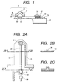
Fig. 1 is a sectional view showing a probe
according to the first embodiment of the present
invention;
Fig. 2A is a top view showing the probe of the
first embodiment, Fig. 2B is a sectional view taken
along a line 2B - 2B in Fig. 2A, and Fig. 2C is a
sectional view taken along a line 2C - 2C in Fig. 2A;
Figs. 3A, 3B, 3C, 3D, 3E, 3F and 3G are sectional
views showing the manufacturing processes of the probe
of the first embodiment;
Fig. 4 is a view showing the arrangement of a
surface observation apparatus using the probe of the
first embodiment;
Fig. 5 is a sectional view showing a probe
according to the second embodiment of the present
invention;
Figs. 6A, 6B, 6C, 6D, 6E, 6F and 6G are sectional
views showing the manufacturing processes of the probe
of the second embodiment;
Fig. 7 is a view showing the arrangement of a
surface observation apparatus using the probe of the
second embodiment;
Fig. 8 is a sectional view showing a probe
according to the third embodiment of the present
invention;
Fig. 9A is a top view showing the probe of the
third embodiment, and Fig. 9B is a sectional view taken
along a line 9B - 9B in Fig. 9A;
Figs. 10A, 10B, 10C, 10D, 10E, 10F and 10G are
sectional views showing the manufacturing processes of
the probe of the third embodiment;
Fig. 11 is a view showing the arrangement of a
recording/reproduction apparatus using the probe of the
third embodiment;
Figs. 12A, 12B, 12C, 12D, 12E and 12F are
sectional views showing the manufacturing processes of
a probe according to the fourth embodiment of the
present invention;
Fig. 13 is a view showing the arrangement of an
exposure apparatus using the probe of the fourth
embodiment; and
Figs. 14A and 14B are views showing the
conventional methods of manufacturing a probe.
DETAILED DESCRIPTION OF THE EMBODIMENTS
The present invention can realize its object with
the above-mentioned arrangements.
The present invention will be described in detail
hereinafter with reference to the accompanying
drawings.
A probe according to the present invention is a
probe for detecting or irradiating evanescent light,
and comprises an elastic member (support member) 10
formed on a substrate 21, a tip 5 for evanescence
formed on the free end portion of the elastic member, a
light-receiving element 19 or laser 20, and a waveguide
28 for optically connecting the light-receiving element
19 or laser 20 and the tip 5.
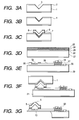
Figs. 3A to 3G are sectional views showing an
example of the manufacturing processes of the probe.
The manufacturing method will be explained below with
reference to Figs. 3A to 3G.
First, a recess portion 3 is formed on the surface
of a first substrate 1 consisting of silicon. In order
to form such recess portion, a protection layer 2 is
formed on the first substrate 1, and a desired portion
of the protection layer 2 is patterned by
photolithography and etching to expose the silicon.
The exposed silicon portion is etched by, e.g.,
crystallographic axis anisotropic etching, so as to
form the recess portion 3. As the protection layer 2,
silicon dioxide or silicon nitride may be used.
Silicon is preferably etched by crystallographic
axis anisotropic etching since it can form a tip 5 with
a sharp distal end. When a potassium hydroxide aqueous
solution or the like is used as an etchant, an inverted
pyramidal recess portion 3 surrounded by four surfaces
equivalent to the (111) face can be formed (see
Fig. 3A).
Second, a peeling layer 4 consisting of an oxide
is formed on the first substrate 1 including the recess
portion 3 (see Fig. 3B).
Since the tip 5 is formed on the peeling layer 4
and is then peeled from the peeling layer 4 in a
process after formation of the peeling layer 4, a
material that allows easy peeling of the material of
the tip 5 must be selected for the peeling layer 4.
More specifically, the material of the peeling layer 4
must have low reactivity and adhesion with the material
of the tip 5.
Such material includes, for example, BN, AlN,
Al2O3, Si3N4, SiO2, TiN, TiO2, VO2, Cr2O3, ZrO2, Ta2O5, WO3,
and the like. These materials can be formed by
sputtering or vacuum evaporation. Especially, when the
first substrate 1 consists of silicon, silicon dioxide
(SiO2) that can be obtained by oxidizing the substrate
surface is preferable.
Third, the tip 5 is formed on the peeling layer
including the recess portion. A light transmission
material is used for a light transmission portion of
the tip 5.
Such material includes inorganic materials such as
SiO2, SiN, or the like, and organic materials such as
polyimide, and the like. When a light transmission
conductive material such as ITO or the like is used,
the obtained probe can be used in an SNOM/STM hybrid
apparatus that measures resistance by applying a
voltage to a sample. When the light transmission layer
itself has insufficient peeling properties from the
peeling layer, a peeling assist layer may be formed on
the surface of the light transmission layer. As such
assist layer, a metal such as Au or the like may be
used. On the other hand, when the light transmission
layer has insufficient adhesion with a bonding layer, a
bonding assist layer may be formed on the interface
with the bonding layer. As such assist layer, a metal
such as Au or the like may be used.
The film formation of the individual materials of
the tip 5 can use vacuum evaporation, sputtering,
chemical vapor deposition, or the like as a thin film
formation technique. After film formation, the
material of the tip 5 is patterned by known
photolithography (Fig. 3C).
Fourth, a light-receiving element or laser and its
waveguide are formed as a light-emitting or
light-receiving mechanism.
Upon forming such components, a known silicon
process or compound semiconductor process may be used
(see Figs. 3D and 3E).
Fifth, a bonding layer 26 is formed on the
substrate 21 or the elastic member 10 formed on the
substrate 21.
The second substrate 21 and elastic member 10
serve as a member for supporting the tip 5 via the
bonding layer 26. The bonding layer bonds the tip 5 by
pressure, and if the tip 5 and bonding layer 26 consist
of metals, a metallic bond can be obtained since they
deform against each other by pressure. Hence, as the
material, a metal, especially, a metal with high
ductility and malleability such as Au, Pt, or the like
is preferable.
Sixth, the material of the tip 5 on the peeling
layer 4 including the recess portion 3 is bonded to the
bonding layer 26. In this process, an alignment
apparatus, which can hold the individual substrates by
vacuum chucks and the like, is used. After the tip 5
on the first substrate 1 and the bonding layer 26 on
the second substrate 21 are aligned to face each other,
they are brought into contact with each other and
pressurized, thus bonding the tip 5 and the bonding
layer 26 (pressure bonding) (Fig. 3F).
Seventh, peeling is done at the interface between
the peeling layer 4 and tip 5 to transfer the material
of the tip 5 onto the bonding layer 26.
More specifically, when the first and second
substrates 1 and 21 are separated away from each other,
the tip 5 is peeled from the peeling layer 4 at their
interface.
Eighth, a micro aperture for detecting or
irradiating light is formed at the distal end of the
tip 5.
For example, the tip distal end portion of the
light transmission layer covered by a metal layer 7 as
a light-shielding layer is brought into contact with a
metal substrate, and a voltage is applied across the
distal end of the tip 5 and the metal substrate via
electrode wiring. Upon application of the voltage, a
coating metal film portion at the distal end of the tip
5 is removed by electric field evaporation or heat
fusion, thus forming a micro aperture.
In practice, a tip, which used Au as the metal
layer 7 and SiO2 as the light transmission layer, was
brought into contact with an Au metal substrate while
controlling the elastic deformation amount of an
elastic cantilever having an elastic constant of 0.1
[N/m] to 1 [µm] or less, i.e., controlling the contact
force to 10-7 [N] or less, and a voltage (crest value:
10 [V], waveform: rectangular wave, time duration: 100
[µs], load resistance: 1 [MΩ]) was applied thereto. As
a result, the micro aperture formed had a diameter of
about 20 [nm].
Alternatively, the tip 5 may be formed to have a
multilayered structure using materials having different
refractive indices, and may be scanned on the sample
surface with a load so as to polish the top surface
layer, thus forming a micro aperture at the waveguide
portion.
The present invention also includes a surface
observation apparatus and recording/reproduction
apparatus using the probe manufactured by the
above-mentioned processes.
This probe is brought close to or into contact
with a sample and is two-dimensionally scanned by an
x-y actuator relative to the sample in the plane of the
sample so as to detect evanescent light leaking out
through the sample surface. In this way, the surface
state of the sample can be observed.
On the other hand, this probe is used to cause
changes in surface state in a micro region on a
recording medium, and such changes in surface state are
observed, thus realizing a recording/reproduction
apparatus. In this case, the SNOM signal itself can be
used in interval control or contact force control with
the sample or recording medium.
When the tip (tip 5) is present on the elastic
member, a technique such as an optical lever,
piezoresistance element, or the like used in an AFM may
be used. Also, a technique used in an STM or a
technique based on the shear force may be used, and
these means do not limit the present invention.
By executing parallel processing of information
using a multi probe that carries a plurality of probes
according to the present invention, a surface
observation apparatus or recording/reproduction
apparatus with a high transfer rate can be provided.
Since the SNOM probe according to the present
invention is formed on the elastic cantilever, the
magnitude of the contact force between the tip (tip 5)
distal end and sample can be controlled to a given
value or less while the tip (tip 5) distal end contacts
the sample.
For example, let k be the elastic constant of the
elastic cantilever, and Δz be the maximum amount of
positional variations of the tip distal end in the
z-direction. Then, since contact force variations
while all tip (tip 5) distal ends contact the surface
of the recording medium or sample are represented by
kΔz, the magnitudes of all the contact forces can be
controlled to kΔz or less by controlling the position
between the second substrate 21 and the recording
medium or sample in the z-direction. In this fashion,
the tip (tip 5) distal end, or the recording medium or
sample can be prevented from being destroyed by an
excessive contact force applied.
The detailed embodiments of the present invention
will be explained below.
[First Embodiment]
The first embodiment is directed to an evanescent
light probe and its manufacturing method according to
the present invention. Figs. 1 and 2A to 2C show the
structure of the probe.
The probe of this embodiment comprises an elastic
lever 10 formed on a substrate 21, a tip 5 which is
formed on the free end portion of the elastic lever and
irradiates evanescent light, a laser 20, and a
waveguide 28 for optically connecting the laser 20 and
the tip 5.
Figs. 3A to 3G are sectional views showing the
manufacturing processes of the evanescent light probe
according to this embodiment.
The manufacturing method will be explained below
with reference to Figs. 3A to 3G.
A (100) single-crystal silicon wafer was prepared
as a first substrate 1.
A 100-nm thick silicon thermal oxide film was
formed as a protection layer 2. A desired portion of
the protection layer 2 was patterned by
photolithography and etching to expose 10-µm2 silicon.
The silicon exposed from the patterned portion was
etched by crystallographic axis anisotropic etching
using an aqueous potassium hydroxide solution.
Note that the etching conditions were: a 30%
aqueous potassium hydroxide solution was used, and a
solution temperature of 90°C and an etching time of 10
min were set.
At this time, a inverted pyramidal recess portion
3 having a depth of about 7 µm and surrounded by four
surfaces equivalent to the (111) plane was formed (see
Fig. 3A).
The thermal oxide film as the protection layer 2
was then removed by an aqueous solution mixture of
hydrogen fluoride and ammonium fluoride (HF : NH4F = 1 :
5). After the removal, the first substrate 1 was
washed using a solution mixture of sulfuric acid and
hydrogen peroxide heated to 120°C, and a 2% aqueous
hydrofluoric acid solution. The first substrate 1 was
heated to 1,000°C in an oxygen/hydrogen atmosphere
using an oxidization oven to deposit a 500-nm thick
silicon dioxide (SiO2) film serving as a peeling layer 4
(see Fig. 3B).
The film formation for the material of the tip 5
was done. A 0.1-µm thick gold (Au) film was formed by
vacuum evaporation to obtain a metal film 7, and a
0.6-µm thick ITO (indium tin oxide) film was formed by
sputtering to obtain a light transmission layer 8.
These films were then patterned by photolithography and
etching. In this case, Au etching used an aqueous
solution mixture of Kl and l2, and ITO etching used an
aqueous solution mixture of HCl and FeCl3. After
patterning, a 0.3-µm thick gold (Au) film was formed
again by vacuum evaporation, and was patterned by
photolithography and etching to obtain a bonding assist
layer 9 (see Fig. 3C).
A 300-µm thick single-crystal n-InP substrate was
used as a second substrate 21, and a 1-µm thick n-InP
buffer layer 22, a 0.1-µm thick InGaAsP active layer
23, a 1.5-µm thick p-InP cladding layer 24, and a
0.3-µm thick p-InGaAs capping layer 25 were formed in
turn on the substrate 21 by MOCVD (metal organic
chemical vapor deposition) (see Fig. 3D).
The obtained multilayered structure was patterned
and etched by photolithography to form a ridge
structure, thus obtaining a laser 20. The wavelength
of the laser formed by the above-mentioned method was
1.3 µm. Etching was done by RIBE (reactive ion beam
etching) using Cl2 gas. A 3-µm thick SiO2 film as a
lever material, insulating layer 27, and mask layer 29
was formed on both surfaces of the structure by
sputtering. The SiO2 films on both surfaces were
patterned and etched by photolithography to form
contact holes, a cantilever structure, and a mask layer
29.
The thickness of the cantilever was 1 µm. A
200-nm thick AuGe film and 300-nm thick Au film were
deposited by vacuum evaporation, and were patterned and
etched by photolithography to form a bonding layer 26,
wiring electrode 33, and output electrode 30 on the
substrate side. A 3-µm thick SIO2 film as a waveguide
28 was deposited by sputtering. The waveguide 28 was
then formed by photolithography and etching. The
etchant used was an aqueous solution mixture of
hydrochloric acid (HCl) and phosphoric acid (H3PO4). In
this case, the projecting portion of the waveguide
formed a secondary diffraction grating. From this
grating, light inside the waveguide can be output
upward. The waveguide 28 had a height of 2 µm and a
width of 5 µm. A 50-nm thick Cr film and 300-nm thick
Au film were deposited by vacuum evaporation, and were
patterned and etched by photolithography to form an
output electrode 31 of the capping layer (see Fig. 3E).
After the tip 5 on the first substrate 1 and the
bonding layer 26 on the second substrate 21 were
aligned to face each other, they were brought into
contact with each other and were pressurized, thus
bonding the tip 5 and the bonding layer 26 (pressure
bonding) (Fig. 3F).
The first and second substrates 1 and 21 were
separated from each other to peel the peeling layer 4
and tip 5 at their interface.
After a protection film was formed on the surface
of the second substrate, the n-InP substrate was etched
from its rear surface using an aqueous HCl solution to
form an SiO2 cantilever. After the formation of the
cantilever, the protection film was removed.
Finally, the tip 5 covered by the metal layer 7
was brought into contact with a metal substrate, and a
voltage was applied across the tip 5 and metal
substrate via the wiring electrode 33 by a voltage
application means.
Upon application of the voltage, a micro aperture
was formed at the tip distal end portion of the metal
layer 7. The diameter of the aperture was about 20 nm
(see Fig. 3G).
Fig. 4 shows the arrangement of an observation
apparatus using the probe of this embodiment. A sample
17 is placed on a holder on an x-y-z scanner. The
probe of this embodiment is set to oppose the sample
17, and x-y scanning is done while the tip 5 contacts
the sample 17.
In this process, evanescent light irradiated from
the tip onto the surface of the sample 17 and reflected
thereby is focused using an objective lens, and is
detected using a photomultiplier, thus allowing surface
observation.
[Second Embodiment]
The second embodiment is directed to another
evanescent light probe and its manufacturing method
according to the present invention.
Fig. 5 shows the structure of the probe. The
probe of this embodiment comprises an elastic lever 10
formed on a substrate 21, a tip 5 which is formed on
the free end portion of the elastic lever and detects
evanescent light, a light-receiving element 19, and a
waveguide 28 for optically connecting the
light-receiving element 19 and the tip 5.
The light-receiving element 19 has the same
structure as that of the laser 20 used in the first
embodiment, and when a reverse electric field is
applied, carriers are excited and a current flows in
response to incoming light. In this way, evanescent
light can be detected. In this embodiment, a plurality
of probes are disposed on the second substrate 21.
Figs. 6A to 6G are sectional views showing the
manufacturing processes of the evanescent light probe
according to this embodiment.
The manufacturing method will be explained below
with reference to Figs. 6A to 6G.
A (100) single-crystal silicon wafer was prepared
as a first substrate 1.
A 100-nm thick silicon thermal oxide film was
formed as a protection layer 2. A desired portion of
the protection layer 2 was patterned by
photolithography and etching to expose 10-µm2 silicon.
The silicon exposed from the patterned portion was
etched by crystallographic axis anisotropic etching
using an aqueous potassium hydroxide solution.
Note that the etching conditions were: a 30%
aqueous potassium hydroxide solution was used, and a
solution temperature of 90°C and an etching time of 10
min were set. At this time, a inverted pyramidal
recess portion 3 having a depth of about 7 µm and
surrounded by four surfaces equivalent to the (111)
plane was formed (see Fig. 6A).
The thermal oxide film as the protection layer 2
was then removed by an aqueous solution mixture of
hydrogen fluoride and ammonium fluoride (HF : NH4F = 1 :
5). After the removal, the first substrate 1 was
washed using a solution mixture of sulfuric acid and
hydrogen peroxide heated to 120°C, and a 2% aqueous
hydrofluoric acid solution. The first substrate 1 was
heated to 1,000°C in an oxygen/hydrogen atmosphere
using an oxidization oven to deposit a 500-nm thick
silicon dioxide (SiO2) film serving as a peeling layer 4
(see Fig. 6B).
The film formation for the material of the tip 5
was done. A 0.1-µm thick gold (Au) film was formed by
vacuum evaporation to obtain a metal film 7, and a
0.6-µm thick ITO (indium tin oxide) film was formed by
sputtering to obtain a light transmission layer 8.
These films were then patterned by photolithography and
etching. In this case, Au etching used an aqueous
solution mixture of Kl and l2 and ITO etching used an
aqueous solution mixture of HCl and FeCl3. After
patterning, a 0.3-µm thick gold (Au) film was formed
again by vacuum evaporation, and was patterned by
photolithography and etching to obtain a bonding assist
layer 9 (see Fig. 6C).
A 300-µm thick single-crystal n-InP substrate was
used as a second substrate 21, and a 1-µm thick n-InP
buffer layer 22, a 0.1-µm thick InGaAsP active layer
23, a 1.5-µm thick p-InP cladding layer 24, and a
0.3-µm thick p-InGaAs capping layer 25 were formed in
turn on the substrate 21 by MOCVD (metal organic
chemical vapor deposition) (see Fig. 6D).
The obtained multilayered structure was patterned
and etched by photolithography to form a ridge
structure, thus obtaining a light-receiving element 19.
Etching was done by RIBE (reactive ion beam etching)
using Cl2 gas. A 3-µm thick SiO2 film as a lever
material, insulating layer 27, and mask layer 29 was
formed on both surfaces of the structure by sputtering.
The SiO2 films on both surfaces were patterned and
etched by photolithography to form contact holes, a
cantilever structure, and a mask layer 29.
The thickness of the cantilever was 1 µm. A
200-nm thick AuGe film and 300-nm thick Au film were
deposited by vacuum evaporation, and were patterned and
etched by photolithography to form a bonding layer 26,
wiring electrode 33, and output electrode 30 on the
substrate side.
In this case, Au etching used ion milling to taper
the waveguide connection portion of the bonding layer.
A 3-µm thick SIO2 film as a waveguide 28 was
deposited by sputtering. The waveguide 28 was then
formed by photolithography and etching. The etchant
used was an aqueous solution mixture of hydrochloric
acid (HCl) and phosphoric acid (H3PO4).
The waveguide 28 had a height of 2 µm and a width
of 5 µm. A 50-nm thick Cr film and 300-nm thick Au
film were deposited by vacuum evaporation, and were
patterned and etched by photolithography to form an
output electrode 31 of the capping layer (see Fig. 6E).
After the tip 5 on the first substrate 1 and the
bonding layer 26 on the second substrate 21 were
aligned to face each other, they were brought into
contact with each other and were pressurized, thus
bonding the tip 5 and the bonding layer 26 (pressure
bonding) (Fig. 6F). The first and second substrates 1
and 21 were separated from each other to peel the
peeling layer 4 and tip 5 at their interface.
After a protection film was formed on the surface
of the second substrate, the n-InP substrate was etched
from its rear surface using an aqueous HCl solution to
form an SiO2 cantilever. After the formation of the
cantilever, the protection film was removed.
Finally, the tip 5 covered by the metal layer 7
was brought into contact with a metal substrate, and a
voltage was applied across the tip 5 and metal
substrate via the wiring electrode 33 by a voltage
application means. Upon application of the voltage, a
micro aperture was formed at the tip distal end portion
of the metal layer 7. The diameter of the aperture was
about 20 nm (see Fig. 6G).
As shown in Figs. 5 and 6A to 6G, in this
embodiment, the micro aperture is formed by forming a
metal layer as a light-shielding layer. The structure
of this embodiment that guides light detected by the
tip toward the light-receiving element does not always
require the light-shielding layer. However, the
light-shielding layer is preferably arranged since the
photodetection resolution can be improved.
Fig. 7 shows the arrangement of an SNOM
observation apparatus using the probes of this
embodiment. A sample 17 is placed on a transparent
substrate on an x-y-z scanner.
Light is irradiated to make an angle that
satisfies the total reflection conditions with the
surface of the sample 17 from the rear side of the
sample 17 via the transparent substrate. At this time,
light is not transmitted upward (Fig. 7) through the
surface of the sample 17, but evanescent light leaks
out through the surface within a very close vicinity
0.1 µm or less from the surface of the sample 17.
When x-y scanning is done while the tip (tip 5)
distal ends of a plurality of SNOM probes contact the
sample 17, the evanescent light components enter the
waveguide 28 via the micro apertures of the SNOM
probes, and are detected by the light-receiving element
19. The detected signals are I/V-converted and are
input to a multiplexer to obtain multi SNOM signals.
By plotting the magnitudes of such SNOM signals,
an SNOM observation image of the sample 17 can be
obtained.
[Third Embodiment]
The third embodiment is directed to still another
evanescent light probe and its manufacturing method
according to the present invention. Figs. 8, 9A and 9B
show the structure of the probe.
The probe of this embodiment comprises an elastic
lever 10 formed on a substrate 21, an evanescent light
tip 5 formed on the free end portion of the elastic
lever, a light-receiving element 19, a laser 20, and a
waveguide 28 for optically connecting the
light-receiving element 19 and laser 20 to the tip 5.
When the laser 20 used in the first embodiment and
the light-receiving element 19 used in the second
embodiment are connected to the tip (tip), return light
of evanescent light irradiated from the tip onto a
recording medium 18 can be detected. In this
embodiment, a plurality of probes are disposed on the
second substrate 21.
Figs. 10A to 10G are sectional views showing the
manufacturing processes of the evanescent light probe
according to this embodiment.
The manufacturing method will be explained below
with reference to Figs. 10A to 10G.
A (100) single-crystal silicon wafer was prepared
as a first substrate 1.
A 100-nm thick silicon thermal oxide film was
formed as a protection layer 2. A desired portion of
the protection layer 2 was patterned by
photolithography and etching to expose 10-µm2 silicon.
The silicon exposed from the patterned portion was
etched by crystallographic axis anisotropic etching
using an aqueous potassium hydroxide solution. Note
that the etching conditions were: a 30% aqueous
potassium hydroxide solution was used, and a solution
temperature of 90°C and an etching time of 10 min were
set. At this time, an inverted pyramidal recess
portion 3 having a depth of about 7 µm and surrounded
by four surfaces equivalent to the (111) plane was
formed (see Fig. 10A).
The thermal oxide film as the protection layer 2
was then removed by an aqueous solution mixture of
hydrogen fluoride and ammonium fluoride (HF : NH4F = 1 :
5).
After the removal, the first substrate 1 was
washed using a solution mixture of sulfuric acid and
hydrogen peroxide heated to 120°C, and a 2% aqueous
hydrofluoric acid solution. The first substrate 1 was
heated to 1,000°C in an oxygen/hydrogen atmosphere
using an oxidization oven to deposit a 500-nm thick
silicon dioxide (SiO2) film serving as a peeling layer 4
(see Fig. 10B).
The film formation for the material of the tip 5
was done. Two different polyimide materials having
different refractive indices were prepared. A
polyimide film a 11, a polyimide film b 12 serving as a
light transmission layer 8, and another polyimide film
a 11 were formed all by spin coating. The obtained
multilayered structure was patterned by
photolithography and etching. In this embodiment,
polyimide was used. Alternatively, silicon oxide films
having different refractive indices may be formed by
sputtering to obtain a layer structure. In this case,
different compositions can be obtained by changing the
O2 flow rate upon sputtering, and films having different
refractive indices can be formed (see Fig. 10C).
A 300-µm thick single-crystal n-InP substrate was
used as a second substrate 21, and a 1-µm thick n-InP
buffer layer 22, a 0.1-µm thick InGaAsP active layer
23, a 1.5-µm thick p-InP cladding layer 24, and a
0.3-µm thick p-InGaAs capping layer 25 were formed in
turn on the substrate 21 by MOCVD (metal organic
chemical vapor deposition) (see Fig. 10D).
The obtained multilayered structure was patterned
and etched by photolithography to form a ridge
structure, thus obtaining a laser 20. Etching was done
by RIBE (reactive ion beam etching) using Cl2 gas. A
3-µm thick SiO2 film as a lever material, insulating
layer 27, and mask layer 29 was formed on both surfaces
of the structure by sputtering. The SiO2 films on both
surfaces were patterned and etched by photolithography
to form contact holes, a cantilever structure, and a
mask layer 29. The thickness of the cantilever was 1
µm.
A 200-nm thick AuGe film and 300-nm thick Au film
were deposited by vacuum evaporation, and were
patterned and etched by photolithography to form a
bonding layer 26, wiring electrode 33, and output
electrode 30 on the substrate side. In this case, Au
etching used ion milling to taper the waveguide
connection portion of the bonding layer.
A 3-µm thick polyimide film serving as a waveguide
28 was deposited by spin coating. The waveguide 28 was
then formed by photolithography and etching.
The waveguide 28 had a height of 2 µm and a width
of 5 µm. A 50-nm thick Cr film and 300-nm Au film were
deposited by vacuum evaporation, and were patterned and
etched by photolithography to form an output electrode
31 of the capping layer (see Fig. 10E).
After the tip 5 on the first substrate 1 and the
bonding layer 26 on the second substrate 21 were
aligned to face each other, they were brought into
contact with each other and were pressurized, thus
bonding the tip 5 and the bonding layer 26 (pressure
bonding) (Fig. 10F). The first and second substrates 1
and 21 were separated from each other to peel the
peeling layer 4 and tip 5 at their interface.
After a protection film was formed on the surface
of the second substrate, the n-InP substrate was etched
from its rear surface using an aqueous HCl solution to
form an SiO2 cantilever.
The tip distal end was polished by scanning the
sample surface to form a micro aperture having a
diameter of about 20 nm on the polyimide layer a 11 to
expose the polyimide layer b 12 therefrom. With this
structure, light is output from the vertex portion of
the polyimide layer b 12. After that, in order to
improve wear resistance, a diamond film was formed on
the probe surface (Fig. 10G).
Fig. 11 shows the arrangement of a
recording/reproduction apparatus using the probes of
this embodiment. A recording medium 18 is placed on a
holder on an x-y-z scanner. The probes of this
embodiment are set to oppose the recording medium 18,
and x-y scanning is done while the tips 5 contact the
recording medium 18. An information recording voltage
signal is demultiplexed by a demultiplexer, and the
demultiplexed signals are supplied to the lasers 20 of
the individual probes via V/I conversion circuits, thus
making the tips 5 emit evanescent light.
Upon recording, the laser beam power is increased
to change the state of the recording medium. Upon
reproduction, the laser beam power is dropped to read
information while maintaining the state of the
recording medium.
As a recording medium used in the
recording/reproduction apparatus, i.e., as an example
of a recording medium whose optical characteristics are
changed by the applied voltage, pentacosa-10,12-diynoic
acid in which upon application of a voltage, the
structure of diacetylene derivative polymer changes by
Joule heat produced by currents that locally flow and
the peak wavelength of the light absorption band
shifts, as described in Japanese Laid-Open Patent
Application No. 4-90152, is known.
On the other hand, as an example of a recording
medium whose optical characteristics change upon
application of a voltage under irradiation of light, an
azo compound having quinone and hydroquinone groups,
which forms redox pairs due to cis-trans
photoisomerization in response to only incoming light
and causes proton movement among these redox pairs upon
application of an electric field, as described in
Japanese Laid-Open Patent Application No. 2-98849, is
known.
[Fourth Embodiment]
This embodiment is directed to an evanescent light
probe and its manufacturing method according to the
present invention. Figs. 12A to 12F show the
manufacturing method and structure of the probe. The
probe of this embodiment comprises an elastic lever 10
formed on a second substrate 21, a tip 5 which is
formed on the free end portion of the elastic lever and
irradiates evanescent light, a surface-emission laser
20 on the surface of a third substrate bonded to the
second substrate 21.
The manufacturing method will be explained below
with reference to Figs. 12A to 12F.
Following the same procedures as in the first
embodiment, a tip 5 made up of a metal layer 7, light
transmission layer 8, and bonding assist layer 9 was
formed (see Figs. 12A, 12B, and 12C).
A 200-µm thick single-crystal silicon substrate
was prepared as a second substrate 21, and a 300-nm
thick silicon dioxide film and 200-nm thick silicon
nitride film were deposited on both surfaces of the
substrate respectively by thermal oxidation and
low-pressure chemical vapor deposition (LPCVD). The
silicon nitride film on the surface was patterned to
have a lever shape. A 5-nm thick chromium film and
50-nm thick gold film were then deposited and were
patterned to form a bonding layer 26 (see Fig. 12D).
After the tip 5 on the first substrate 1 and the
bonding layer 26 on the second substrate 21 were
aligned to face each other, they were brought into
contact with each other and were pressurized, thus
bonding the tip 5 and the bonding layer 26 (pressure
bonding) (Fig. 12E).
The first and second substrates 1 and 21 were
separated from each other to peel the peeling layer 4
and tip 5 at their interface. The silicon dioxide film
and silicon nitride film on the rear surface were
patterned to form an opening. After a protection film
was formed on the surface, the second substrate 21 was
etched using an aqueous potassium hydroxide solution,
and the silicon dioxide film on the surface was also
etched, thus forming a lever 10.
The tip distal end was polished by scanning the
sample surface with a load to form a micro aperture
having a diameter of about 20 nm on the metal layer 7,
thus exposing the light transmission layer 8 therefrom.
Subsequently, a third substrate 119, on which
light-emitting elements 116 comprising surface-emission
lasers were disposed in a matrix at a position
corresponding to the tip 5 on the second substrate 21,
was prepared. The third substrate 119 is obtained by
forming anodes 123, cathode 124, active layer 125,
mirror layers 126, silicon nitride layer 127, and
polyimide layer 128 on a gallium arsenide substrate.
The anodes 123 are connected to the individual
light-emitting elements 116 to independently drive
them. The silicon nitride layer 127 is formed to
attain insulation of the anode 123. The cathode 124 is
a common electrode. When a voltage is applied across
the anode 123 and cathode 124, a laser beam produced in
the active layer 125 is reflected by the upper and
lower mirror layers 126, and is emitted from the upper
opening. After the third substrate was prepared, the
second and third substrates 21 and 119 were bonded to
each other using an epoxy resin 118 after they were
aligned so that laser beams coming from the
light-emitting elements 116 were directly guided to the
tip 5 and the opening (see Fig. 12F).
The multi light probe was manufactured by the
above-mentioned processes.
Fig. 13 shows the arrangement of an exposure
apparatus using the multi probe of this embodiment. A
substrate applied with photoresist is placed on a
holder on an x-y-z scanner. The probe of this
embodiment is set to oppose the photoresist, and x-y
scanning is done while the tip 5 contacts the
photoresist. By ON/OFF-controlling evanescent light to
be irradiated from the tip 5 onto the photoresist
surface, a micropattern can be formed, and high
exposure speed can be realized.
This embodiment has exemplified the probe
structure that directly guides light coming from each
light-emitting element to the tip. Alternatively, as
in the second embodiment, a light-receiving element may
be formed in place of the light-emitting element, and
light detected by the tip may be directly guided to the
light-receiving element. In this case, the
light-shielding layer with a micro aperture is not
always required, as in the second embodiment.
In the above-mentioned embodiments, the tip is
supported by the cantilever. However, the present
invention is not limited to such specific support
structure. For example, a double-supported lever type,
torsion lever type, or the like may be used as the
support structure. In case of the cantilever type and
double-supported lever type, the support member must be
an elastic member, but in case of the torsion lever
type, the support member is not limited to an elastic
member.