EP0854571A2 - Surface acoustic wave filter - Google Patents
Surface acoustic wave filter Download PDFInfo
- Publication number
- EP0854571A2 EP0854571A2 EP98100749A EP98100749A EP0854571A2 EP 0854571 A2 EP0854571 A2 EP 0854571A2 EP 98100749 A EP98100749 A EP 98100749A EP 98100749 A EP98100749 A EP 98100749A EP 0854571 A2 EP0854571 A2 EP 0854571A2
- Authority
- EP
- European Patent Office
- Prior art keywords
- piezoelectric substrate
- acoustic wave
- surface acoustic
- type surface
- transversal
- Prior art date
- Legal status (The legal status is an assumption and is not a legal conclusion. Google has not performed a legal analysis and makes no representation as to the accuracy of the status listed.)
- Granted
Links
- 238000010897 surface acoustic wave method Methods 0.000 title claims abstract description 30
- 239000000758 substrate Substances 0.000 claims abstract description 105
- 230000000644 propagated effect Effects 0.000 claims abstract description 5
- 230000008878 coupling Effects 0.000 claims description 4
- 238000010168 coupling process Methods 0.000 claims description 4
- 238000005859 coupling reaction Methods 0.000 claims description 4
- 238000003780 insertion Methods 0.000 description 9
- 230000037431 insertion Effects 0.000 description 8
- 239000010408 film Substances 0.000 description 6
- 230000000052 comparative effect Effects 0.000 description 4
- 230000001902 propagating effect Effects 0.000 description 4
- 239000010409 thin film Substances 0.000 description 3
- XAGFODPZIPBFFR-UHFFFAOYSA-N aluminium Chemical compound [Al] XAGFODPZIPBFFR-UHFFFAOYSA-N 0.000 description 2
- 229910052782 aluminium Inorganic materials 0.000 description 2
- 239000000919 ceramic Substances 0.000 description 2
- 239000013078 crystal Substances 0.000 description 2
- 230000003247 decreasing effect Effects 0.000 description 2
- 229910003327 LiNbO3 Inorganic materials 0.000 description 1
- 229910012463 LiTaO3 Inorganic materials 0.000 description 1
- 239000003082 abrasive agent Substances 0.000 description 1
- 230000015572 biosynthetic process Effects 0.000 description 1
- 230000006866 deterioration Effects 0.000 description 1
- 238000006073 displacement reaction Methods 0.000 description 1
- HFGPZNIAWCZYJU-UHFFFAOYSA-N lead zirconate titanate Chemical compound [O-2].[O-2].[O-2].[O-2].[O-2].[Ti+4].[Zr+4].[Pb+2] HFGPZNIAWCZYJU-UHFFFAOYSA-N 0.000 description 1
- 238000000034 method Methods 0.000 description 1
- 238000007788 roughening Methods 0.000 description 1
Images


Classifications
-
- H—ELECTRICITY
- H03—ELECTRONIC CIRCUITRY
- H03H—IMPEDANCE NETWORKS, e.g. RESONANT CIRCUITS; RESONATORS
- H03H9/00—Networks comprising electromechanical or electro-acoustic elements; Electromechanical resonators
- H03H9/46—Filters
- H03H9/64—Filters using surface acoustic waves
- H03H9/6423—Means for obtaining a particular transfer characteristic
- H03H9/6433—Coupled resonator filters
-
- H—ELECTRICITY
- H03—ELECTRONIC CIRCUITRY
- H03H—IMPEDANCE NETWORKS, e.g. RESONANT CIRCUITS; RESONATORS
- H03H3/00—Apparatus or processes specially adapted for the manufacture of impedance networks, resonating circuits, resonators
- H03H3/007—Apparatus or processes specially adapted for the manufacture of impedance networks, resonating circuits, resonators for the manufacture of electromechanical resonators or networks
- H03H3/08—Apparatus or processes specially adapted for the manufacture of impedance networks, resonating circuits, resonators for the manufacture of electromechanical resonators or networks for the manufacture of resonators or networks using surface acoustic waves
- H03H3/10—Apparatus or processes specially adapted for the manufacture of impedance networks, resonating circuits, resonators for the manufacture of electromechanical resonators or networks for the manufacture of resonators or networks using surface acoustic waves for obtaining desired frequency or temperature coefficient
-
- H—ELECTRICITY
- H03—ELECTRONIC CIRCUITRY
- H03H—IMPEDANCE NETWORKS, e.g. RESONANT CIRCUITS; RESONATORS
- H03H9/00—Networks comprising electromechanical or electro-acoustic elements; Electromechanical resonators
- H03H9/02—Details
- H03H9/02535—Details of surface acoustic wave devices
- H03H9/02637—Details concerning reflective or coupling arrays
- H03H9/02669—Edge reflection structures, i.e. resonating structures without metallic reflectors, e.g. Bleustein-Gulyaev-Shimizu [BGS], shear horizontal [SH], shear transverse [ST], Love waves devices
-
- H—ELECTRICITY
- H03—ELECTRONIC CIRCUITRY
- H03H—IMPEDANCE NETWORKS, e.g. RESONANT CIRCUITS; RESONATORS
- H03H9/00—Networks comprising electromechanical or electro-acoustic elements; Electromechanical resonators
- H03H9/46—Filters
- H03H9/64—Filters using surface acoustic waves
- H03H9/6423—Means for obtaining a particular transfer characteristic
- H03H9/6433—Coupled resonator filters
- H03H9/644—Coupled resonator filters having two acoustic tracks
- H03H9/6456—Coupled resonator filters having two acoustic tracks being electrically coupled
- H03H9/6459—Coupled resonator filters having two acoustic tracks being electrically coupled via one connecting electrode
- H03H9/6463—Coupled resonator filters having two acoustic tracks being electrically coupled via one connecting electrode the tracks being electrically cascaded
-
- H—ELECTRICITY
- H03—ELECTRONIC CIRCUITRY
- H03H—IMPEDANCE NETWORKS, e.g. RESONANT CIRCUITS; RESONATORS
- H03H9/00—Networks comprising electromechanical or electro-acoustic elements; Electromechanical resonators
- H03H9/02—Details
- H03H9/02244—Details of microelectro-mechanical resonators
- H03H9/02259—Driving or detection means
- H03H9/02275—Comb electrodes
-
- H—ELECTRICITY
- H03—ELECTRONIC CIRCUITRY
- H03H—IMPEDANCE NETWORKS, e.g. RESONANT CIRCUITS; RESONATORS
- H03H9/00—Networks comprising electromechanical or electro-acoustic elements; Electromechanical resonators
- H03H9/02—Details
- H03H9/02535—Details of surface acoustic wave devices
- H03H9/02614—Treatment of substrates, e.g. curved, spherical, cylindrical substrates ensuring closed round-about circuits for the acoustical waves
- H03H9/02622—Treatment of substrates, e.g. curved, spherical, cylindrical substrates ensuring closed round-about circuits for the acoustical waves of the surface, including back surface
-
- H—ELECTRICITY
- H03—ELECTRONIC CIRCUITRY
- H03H—IMPEDANCE NETWORKS, e.g. RESONANT CIRCUITS; RESONATORS
- H03H9/00—Networks comprising electromechanical or electro-acoustic elements; Electromechanical resonators
- H03H9/02—Details
- H03H9/02535—Details of surface acoustic wave devices
- H03H9/02637—Details concerning reflective or coupling arrays
- H03H9/02779—Continuous surface reflective arrays
-
- H—ELECTRICITY
- H03—ELECTRONIC CIRCUITRY
- H03H—IMPEDANCE NETWORKS, e.g. RESONANT CIRCUITS; RESONATORS
- H03H9/00—Networks comprising electromechanical or electro-acoustic elements; Electromechanical resonators
- H03H9/02—Details
- H03H9/02535—Details of surface acoustic wave devices
- H03H9/02818—Means for compensation or elimination of undesirable effects
- H03H9/02842—Means for compensation or elimination of undesirable effects of reflections
Definitions
- the present invention relates to a surface acoustic wave filter utilizing shear horizontal type (SH type) surface acoustic waves, and more particularly, to a transversal-coupled resonator type surface acoustic wave (hereinafter referred to as SAW) filter.
- SH type shear horizontal type
- SAW transversal-coupled resonator type surface acoustic wave
- Transversal-coupled resonator type double mode SAW filters utilizing Rayleigh waves are known.
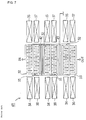
- An example of this type of lateral coupling type SAW filter will be described with reference to Fig. 6.
- FIG. 6 is a simplified plan view for explaining a configuration of electrodes of a conventional transversal-coupled resonator type SAW filter using Rayleigh waves.
- a SAW filter 31 has a structure wherein first and second interdigital transducers (hereinafter abbreviated to read "IDTs") 32 and 33 are provided on a piezoelectric substrate (not shown) and grating reflectors 34, 35, 36, 37 are provided on both sides of the IDTs 32 and 33.
- IDTs first and second interdigital transducers
- the IDT 32 includes a pair of comb-shaped electrodes 32a, 32b each having at least one electrode finger.
- the comb-shaped electrode 32a and the comb-shaped electrode 32b are arranged such that their electrode fingers are interdigitated with each other.
- the IDT 33 includes a pair of comb-shaped electrodes 33a and 33b.
- the space between adjacent electrode fingers of the IDTs 32 and 33 is set to be ⁇ /4, and the width of each electrode finger is set to be ⁇ /4.
- ⁇ represents the wavelength of a surface acoustic wave to be excited in the surface acoustic wave filter.
- the comb-shaped electrode 32b of the IDT 32 and the comb-shaped electrode 33a of the IDT 33 share a common bus.
- the comb-shaped electrode 32a of the IDT 32 is the input electrode and the comb-shaped electrode 33b of the other IDT 33 is the output electrode of the SAW filter 31.
- the comb-shaped electrodes 32b and 33a are grounded.
- the SAW filter 31 operates as a transversal-coupled resonator type double mode SAW filter.
- first and second IDTs 32 and 33 of the SAW filter 31 shown in Fig. 6 are coupled in a direction perpendicular to the propagating direction of surface acoustic waves, i.e., in a lateral direction
- a configuration is also known in which a plurality of SAW resonators having the above-described first and second IDTs 32 and 33 are further coupled in the lateral direction.
- transversal-coupled resonator type SAW filters having IDTs 32 and 33 are transversally coupled to each other in the form of three stages.
- the configuration of each of the IDTs and reflectors is the same as that in the SAW filter 31 shown in Fig. 6.
- a comb-shaped electrode of IDT 32 of the upper stage is used as the input end as illustrated, and an outer comb-shaped electrode of an IDT 33 of the SAW filter at the final stage is used as the output electrode.
- Conductive patterns 42 and 43 connected to the ground potential are provided between the stages, and the conductive patterns 42 and 43 are connected to a bus bar which is connected to the ground potential of the SAW filter at each stage.
- reflectors 34 through 37 have been required on both sides of IDTs 31 and 32 in order to produce a standing wave.
- Such reflectors have a structure in which a multiplicity of electrodes fingers are short-circuited or open-circuited. Therefore, it has been necessary to increase the dimensions of the substrate according to an amount required for providing the reflectors 34 through 37.
- the object of the present invention is directed to a transversal-coupled resonator type SAW filter as known which can be formed with smaller overall dimensions and which has wider band characteristics.
- a transversal-coupled resonator type SAW filter that overcomes the above-described problems of the prior art provides a transversal-coupled resonator type SAW filter having a reduced size and providing increased band characteristics.
- a transversal-coupled resonator type SAW filter according to a preferred embodiment of the present invention includes a piezoelectric substrate and first and second interdigital transducers.
- the piezoelectric substrate has a pair of substrate edges which are substantially parallel to each other and reflect a shear horizontal type surface wave which is excited and propagated on a surface of the piezoelectric substrate in a direction which is substantially perpendicular to the substrate edges.
- the first and second interdigital transducers have the same resonance characteristics and are provided on the piezoelectric substrate.
- Each of the first and second interdigital transducers includes a pair of outermost electrode fingers which are arranged to be flush with the substrate edges of the piezoelectric substrate, respectively and a pair of adjacent electrode fingers which are adjacent to the pair of the outermost electrode fingers, respectively.
- a distance D' from one of the substrate edges of the piezoelectric substrate to a center of the corresponding adjacent electrode finger satisfies the following inequalities: where ⁇ is a wavelength of the shear horizontal type surface acoustic wave excited on the piezoelectric substrate.
- a plurality of the above-described transversal-coupled resonator type SAW filters are arranged on the same substrate to provide a multi-stage connection type SAW filter.
- the piezoelectric substrate preferably has a roughened back surface.
- the roughened back surface may have a plurality of grooves provided therein.
- the first and second interdigital transducers preferably include first and second comb-shaped electrodes each having a bus bar and a plurality of electrode fingers connected to the bus, the first and second comb-shaped electrodes being interdigitated with each other.
- the second comb-shaped electrode of the first interdigital transducer is arranged to share the bus bar of the first comb-shaped electrode of the second interdigital transducer.
- the pair of outermost electrode fingers preferably have a width w' which satisfies the following inequalities:
- a transversal-coupled resonator type double mode SAW filter is configured utilizing an SH type surface wave and as a substrate edge reflection type surface wave device, there is no need for providing reflectors on both sides of IDTs. This makes it possible to significantly reduce the size of a SAW filter.
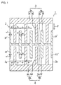
- Fig. 1 is a plan view for explaining a SAW filter according to a preferred embodiment of the present invention.
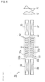
- Fig. 2 is a bottom view of a piezoelectric substrate of the SAW filter shown in Fig. 1.
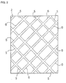
- Fig. 3 is a schematic plan view for explaining a SAW filter in which three stages of SAW filters are connected in a lateral direction according to another preferred embodiment of the present invention.
- Fig. 4 is a graph showing the frequency-insertion loss characteristics of the SAW filter shown in Fig. 1.
- Fig. 5 is a graph showing the insertion loss-frequency characteristics of a SAW filter according to a comparative example.
- Fig. 6 is a schematic plan view for explaining an example of a conventional transversal-coupled resonator type double mode SAW filter.
- Fig. 7 is a schematic plan view for explaining another example of a conventional transversal-coupled resonator type double mode SAW filter.
- a SAW filter according to preferred embodiments of the invention is a transversal-coupled resonator type double mode SAW filter utilizing an SH type surface wave.
- an SH type surface wave means a surface wave whose displacement is substantially perpendicular to the propagating direction of the surface wave and is parallel to the surface of the substrate.
- SH type surface waves include SH type leaky waves, Love waves and BGS (Bleustein-Gulyaev-Shimizu) waves.
- Fig. 1 shows a plan view of an SAW filter 1 according to a first preferred embodiment of the present invention.
- the SAW filter 1 includes a piezoelectric substrate 2, a first IDT 3 and a second IDT 4.
- the piezoelectric substrate 2 is preferably formed of a piezoelectric single crystal such as an LiTaO 3 and an LiNbO 3 or PZT type piezoelectric ceramics.
- the piezoelectric substrate 2 has a substantially rectangular planar shape and includes a pair of substrate edges 2a and 2b which are preferably substantially parallel to each other.
- the piezoelectric substrate 2 is polarized in the direction of the arrow P which is substantially parallel to the end surfaces 2a and 2b.
- the first and second IDTs 3 and 4 are disposed on the upper surface of the piezoelectric substrate 2.
- the first and second IDTs 3 and 4 preferably have the same resonance characteristics and are arranged in a direction substantially parallel to the substrate edges 2a and 2b so as to be located between the substrate edges 2a and 2b.
- the IDT 3 includes comb-shaped electrodes 3a and 3b each having one or more electrode fingers.
- the comb-shaped electrode 3a comprises a bus bar 3c and electrode fingers 3d connected to the bus bar 3c
- the comb-shaped electrode 3b comprises a bus bar 3e and electrode fingers 3f connected to the bus bar 3e.
- the IDT 3 is arranged on the piezoelectric substrate 2 such that the electrode fingers 3d of the comb-shaped electrodes 3a and the electrode fingers 3f of the comb-shaped electrodes 3b extend in a direction substantially parallel to the substrate edges 2a and 2b and are interdigitated between each other.
- a pair of outermost fingers 3f' of the IDT 3 extending in the propagating direction of a surface wave are preferably arranged to be flush with the substrate edges 2a and 2b, respectively.
- the outermost fingers of the comb-shaped electrode 3b are the outermost electrode fingers 3f' of IDT 3
- the outermost electrode fingers of the comb-shaped electrode 3a may be arranged to be flush with the substrate edges 2a and 2b. In this case, the outermost fingers of the comb-shaped electrode 3a become the outermost electrode fingers of the IDT 3.
- one outermost finger of the comb-shaped electrode 3a is arranged to be flush with either the substrate edge 2a or 2b
- one outermost electrode finger of the comb-shaped electrode 3b may be arranged to be flush with either the substrate edge 2b or 2a. That is, the IDT 3 has a pair of outermost fingers which are arranged to be flush with the substrate edge 2a and 2b, respectively, regardless of the outermost fingers, whereby both ends of the IDT 3 are flush with the substrate edge 2a and 2b of the piezoelectric substrate 2, respectively.
- the IDT 4 includes comb-shaped electrodes 4a and 4b each having one or more electrode fingers.
- the number of the pair of electrode fingers in IDT 4 is preferably set to be the same as that in the IDT 3 so that the IDTs 3 and 4 have the same resonance characteristics.
- the comb-shaped electrode 4a comprises a bus bar 4c and electrode fingers 4d connected to the bus bar 4c.
- the comb-shaped electrode 4b comprises the bus bar 3e and electrodes fingers 4f connected to the bus bar 3e.
- the bus bar 3e is shared between the comb-shaped electrode 4b and the comb-shaped electrode 3b.
- the IDT 4 is arranged on the piezoelectric substrate 2 such that the electrode fingers 4d of the comb-shaped electrodes 4a and the electrode fingers 4f of the comb-shaped electrodes 4b extend in a direction substantially parallel to the substrate edges 2a and 2b and are interdigitated with each other.
- Outermost fingers 4f' of the IDT 4 extending in the propagating direction of a surface wave are arranged to be flush with the substrate edges 2a and 2b.
- One or a pair of outermost electrode fingers of the comb-shaped electrode 4a may be arranged to be flush with the substrate edge 2a and/or 2b in accordance with the configuration of the IDT 3.
- the IDT 4 also has a pair of outermost fingers which are flush with the substrate edge 2a and 2b, respectively, regardless of the outermost fingers, whereby both ends of the IDT 4 are flush with the substrate edge 2a and 2b of the piezoelectric substrate 2, respectively.
- an electrode finger distance D defined by a distance from the center of one of the electrode fingers to the center of the adjacent electrode finger is preferably set to be equal to about ⁇ /2, where ⁇ is the wavelength of the SH type surface wave excited on the substrate 2.
- the outermost electrode finger distance D' defined by a distance from the substrate edge 2a or 2b to the center of the electrode finger adjacent to the outermost electrode finger 3f' or 4f' is preferably set to be a value defined by the following inequalities:
- each electrode finger distance i.e., the distance D and the distance D'
- each electrode finger distance D and the distance D' must be set to be ⁇ /2 so that a standing wave exists on a SAW device.
- the inventors of the present invention have first found that the outermost electrode finger distance D' can be changed from ⁇ /2 without causing substantial deterioration in the filter characteristic and that the filter characteristic is improved if the distance D' satisfies the aforementioned inequalities. The feature will be explained in detail in the specific example below.
- the distance L between the substrate edge 2a and the substrate edge 2b is therefore preferably set to be a value defined by the following inequalities: where n is an integer equal to 1 or more.
- the width w of the electrode fingers and the space gap s between the electrode fingers are set to be the same i.e., to be about ⁇ /4
- the width w' of the outermost fingers 3f' and 4f' is preferably set to be a value defined by the following inequalities.
- the piezoelectric substrate 2 of the SAW filter 1 has a plurality of grooves 5 and 6 located on the back surface of the piezoelectric substrate 2.
- the formation of the grooves 5 and 6 roughens the surface of the piezoelectric substrate which is opposite to the side on which the IDTs 3, 4 are located.
- the number and arrangement of the grooves are not limited to that illustrated in Fig. 2, and the back surface may be roughened by a method other than forming grooves. Random recesses may be formed on the back surface of the piezoelectric substrate 2.
- the back surface of the piezoelectric substrate 2 may be ground with an abrasive material or grinding attachment to provide the roughened surface.
- the comb-shaped electrode 3a of the IDT 3 and the comb-shaped electrode 4a of the IDT 4 are used as the input and output ends, respectively, and the comb-shaped electrodes 3b and 4b are connected to the ground potential.
- BGS waves are excited on the piezoelectric substrate 2.
- the excited BGS waves are propagated in the direction which is substantially perpendicular to the substrate edge 2a and substrate edge 2b and reflected by the substrate edges 2a and 2b, whereby a fundamental wave and higher-order mode waves of the excited BGS waves are coupled with each other to produce a standing wave between the substrate edges 2a and 2b.
- the SAW filter 1 can operate as a transversal-coupled resonator type double mode SAW filter utilizing a BGS wave.
- the SAW filter 1 it is not required to provide reflectors outside the IDTs 3 and 4. It is therefore possible to make the piezoelectric substrate 2 small. Further, since no reflector is used, it is possible to prevent the stop band from being affected by the reflection characteristics of reflectors and to prevent the surface acoustic wave from decaying between the IDT and reflectors and therefore to realize a SAW filter having a wide band and a small insertion loss.
- the distance D' defined by a distance from the substrate edge 2a or 2b to the center of the electrode finger adjacent to the outermost electrode finger 3f' or 4f' is set to be the above-mentioned specific value so as to suppress unwanted ripples in the passband. This will be explained in detail later.
- a SAW filter 11 includes SAW filters 1a, 1b and 1c extending in a direction substantially parallel to two substrate edges 2a and 2b of the piezoelectric substrate 2.
- the SAW filters 1a, 1b and 1c respectively comprise IDTs 13a and 14a, 13b and 14b and 13c and 14c provided on the piezoelectric substrate 2 as explained in detail with reference to Fig. 1.
- Conductive patterns 12 and 15 connected to the ground potential are provided between the SAW filters 1a and 1b, and 1b and 1c.
- the conductive patterns 12 and 15 and the comb-shaped electrodes 3b and 4a may be grounded in common to a connection conductive portion (not shown) provided on the piezoelectric substrate or may be separately grounded.
- the comb-shaped electrode 4b of the IDT 14a and comb-shaped electrode 3a of the IDT 13b, and the comb-shaped electrode 4b of the IDT 14b and comb-shaped electrode 3a of the IDT 13c may be electrically connected respectively through either wires 16 and 17 or conductive patterns (not shown) on the piezoelectric substrate 2.
- the piezoelectric substrate 2 may have a roughened surface as explained above.
- the SAW filter 11 since the three stages of SAW filters 1a, 1b and 1c are provided, the amount of the attenuation can be increased. Further, the conductive patterns 12 and 15 connected to the ground potential can reduce spurious response.
- the piezoelectric substrate 2 of the SAW filter 1 or 11 is preferably made of piezoelectric single crystal, or piezoelectric ceramics
- the piezoelectric substrate 2 may be an insulating substrate having a piezoelectric thin film, such as ZnO, thereon.
- an insulating film or the like may be further interposed between the insulating substrate and the piezoelectric thin film.
- a piezoelectric substrate having thereon a thin film such as piezoelectric film, dielectric film, insulating film or the like.
- other SH type surface waves such as Love waves and leaky surface acoustic waves may be used other than BGS waves.
- a specific example of at least one preferred embodiment of the present invention will be described with reference to Fig. 3.
- a three-stage connection type SAW filter shown in Fig. 3 is manufactured.
- a substrate made of lead titanate zirconate and having a thickness of 0.5 mm and dimensions of 2.2 x 1.8 mm is prepared as a piezoelectric substrate 2.
- the aluminum film is etched using a mask so as to form IDTs 13a, 13b, 13c 14a, 14b and 14c having comb-shaped electrodes 3a and 3b, and 4a and 4b on the piezoelectric substrate 2.
- the number of pairs of the electrodes finger is set to be 34 for all the IDTs 13a, 13b, 13c 14a, 14b and 14c.
- the space between the electrode fingers and the width of the electrodes fingers except the outermost electrode fingers are set to be 9.8 ⁇ m ( ⁇ /4), and the electrode finger distance is set 19.6 ⁇ m ( ⁇ /2).
- the width of the outermost electrode fingers is set to be 4.92 ⁇ m which corresponds to (2.01 ⁇ )/16 and satisfies the inequalities (3).
- the distance D' is set to be 19.62 ⁇ m (8.01 ⁇ /16) and satisfies the inequalities (1).
- An SAW filter according to a conventional comparative example is fabricated similarly to the SAW filter according to the inventive example described above except that the width of the outermost electrode fingers 3f' and 4f' is set to be 2.45 ⁇ m which corresponds to ⁇ /16. In the case, the distance D' is set to be 17.15 ⁇ m (7 ⁇ /16). Therefore, the width of the outermost electrode finger and the distance D' are out of the ranges defined by the inequalities (3) and (1), respectively.
- Fig. 4 shows insertion loss-frequency characteristics of the SAW filter according to the inventive example.
- a bandpass filter having a passband in the range from 64.77 to 65.43 MHz can be configured using the SAW filter of the inventive example.
- insertion loss in the passband is 4 dB and that the 3 dB bandwidth (the bandwidth within which insertion loss stays within 3 dB from the minimum insertion loss) is 1 % of the center frequency of the filter. It has been confirmed that the SAW filter has the filter characteristics in which the attenuations at 64.2 MHz and 66.4 MHz are 46 dB and 25 dB, respectively. It is also apparent from Fig. 4, there are no substantial ripples within the passband.
- the preferred embodiments of the present invention make it possible to configure a transversal-coupled resonator type SAW filter having a wide passband and to suppress ripples in the passband effectively.
- the distance D' defined by a distance from the substrate edge 2a or 2b to the center of the electrode finger adjacent to the outermost electrode finger 3f' or 4f' (Fig. 1) is set to be equal to or less than ⁇ /2, substantial ripples are generated in the passband.
- the outermost electrode finger distance D' is set to be greater than ( ⁇ /2 + (5 ⁇ )/16), the amount of the attenuation of the obtained SAW filter is decreased. Accordingly, it is preferable to set the outermost electrode finger distance D' at the value defined by the inequalities (1).
- the width of the electrode fingers other than the outermost electrode fingers and the space between the electrode fingers are set to be the same, i.e., to be about ⁇ /4, it has been confirmed that the width of the electrode fingers other than the outermost electrode fingers may be greater than the space between the electrode (i.e., greater than about ⁇ /4) as long as the outermost electrode finger distance is equal to the value defined by the inequalities (1).
Landscapes
- Physics & Mathematics (AREA)
- Acoustics & Sound (AREA)
- Engineering & Computer Science (AREA)
- Manufacturing & Machinery (AREA)
- Surface Acoustic Wave Elements And Circuit Networks Thereof (AREA)
Abstract
Description

Claims (8)
- A transversal-coupled resonator type surface acoustic wave filter comprising:a piezoelectric substrate (2) having a pair of substrate edges (2a, 2b) which are substantially parallel to each other and which are arranged to reflect a shear horizontal type surface wave excited and propagated on a surface of the piezoelectric substrate in a direction substantially perpendicular to the substrate edges (2a, 2b);first and second interdigital transducers (3, 4) having a common resonance characteristic and provided on the piezoelectric substrate,
characterized in that
each of the first and second interdigital transducers (3, 4) include a pair of outermost electrode fingers (3f', 4f') each of which is arranged to be flush with a respective one of the substrate edges (2a, 2b) of the piezoelectric substrate (2), and a pair of adjacent electrode fingers (3a, 4a) which are adjacent to the pair of the outermost electrode fingers (3f', 4f'), respectively;
wherein
a distance D' from one of the substrate edges of the piezoelectric substrate to a center of the corresponding adjacent electrode finger satisfies the following inequalities:where λ is a wavelength of the shear horizontal type surface acoustic wave excited on the piezoelectric substrate.
- A transversal-coupled resonator type surface acoustic wave filter according to claim 1, characterized in that the piezoelectric substrate has a roughened back surface.
- A transversal-coupled resonator type surface acoustic wave filter according to claim 2, characterized in that the roughened back surface has a plurality of grooves (5, 6) formed thereon.
- A transversal-coupled resonator type surface acoustic wave filter according to one of the claims 1 to 3, characterized in that each of the first and second interdigital transducers (3, 4) includes first and second comb-shaped electrodes (3a, 4a, 3b, 4b) each having a bus (3c, 4c, 3e) and a plurality of electrode fingers (3d, 3f, 4d, 4f) connected to the bus bar (3c, 4c, 3e), the first and second comb-shaped electrodes (3a, 3b; 4a, 4b) being interdigitated with each other, the second comb-shaped electrodes (3f) of the first interdigital transducer (3) sharing the bus bar (3e) of the first comb-shaped electrode (4f) of the second interdigital transducer (4).
- A transversal-coupled resonator type surface acoustic wave filter according to one of the claims 1 to 4, characterized in that each of the pair of outermost electrode fingers (3f', 4f') have a width w' which satisfies the following inequalities:

- A transversal-coupled resonator type surface acoustic wave filter according to one of the claims 1-5, characterized by
a plurality of transversal-coupled resonator type surface acoustic wave filter units (1a, 1b, 1c) electrically connected to each other and disposed on the piezoelectric substrate (2), the plurality of transversal-coupled resonator type surface acoustic wave filter units (1a, 1b, 1c) being arranged in a direction substantially parallel to the substrate edges (2a, 2b) of the piezoelectric substrate (2), each of the lateral coupling type surface acoustic wave filter units (1a, 1b, 1c) including the first and second interdigital transducers (13a, 14a, 13b, 14b, 13c, 14c) having a common resonance characteristic and provided on the piezoelectric substrate (2). - A transversal-coupled resonator type surface acoustic wave filter according to claim 6, further including a conductive pattern located between the plurality of transversal-coupled resonator type surface acoustic wave filter units (1a, 1b, 1c), the conductive pattern being disposed on the piezoelectric substrate (2) and arranged to be connected to a ground level.
- A transversal-coupled type surface acoustic wave filter according to claim 6 or 7, characterized in that each of the first and second interdigital transducers of each of the lateral coupling type surface acoustic wave filter units (1a, 1b, 1c) includes first and second comb-shaped electrodes each having a bus and a plurality of electrode fingers connected to the bus, the first and second comb-shaped electrodes being interdigitated with each other, the second comb-shaped electrodes of the first interdigital transducer sharing the bus of the first comb-shaped electrode of the second interdigital transducer.
Applications Claiming Priority (6)
| Application Number | Priority Date | Filing Date | Title |
|---|---|---|---|
| JP7812/97 | 1997-01-20 | ||
| JP781297 | 1997-01-20 | ||
| JP781297 | 1997-01-20 | ||
| JP357790/97 | 1997-12-25 | ||
| JP35779097A JP3233087B2 (en) | 1997-01-20 | 1997-12-25 | Surface acoustic wave filter |
| JP35779097 | 1997-12-25 |
Publications (3)
| Publication Number | Publication Date |
|---|---|
| EP0854571A2 true EP0854571A2 (en) | 1998-07-22 |
| EP0854571A3 EP0854571A3 (en) | 2000-07-26 |
| EP0854571B1 EP0854571B1 (en) | 2008-09-03 |
Family
ID=26342185
Family Applications (1)
| Application Number | Title | Priority Date | Filing Date |
|---|---|---|---|
| EP98100749A Expired - Lifetime EP0854571B1 (en) | 1997-01-20 | 1998-01-16 | Surface acoustic wave filter |
Country Status (6)
| Country | Link |
|---|---|
| US (1) | US5977686A (en) |
| EP (1) | EP0854571B1 (en) |
| JP (1) | JP3233087B2 (en) |
| KR (1) | KR100280609B1 (en) |
| DE (1) | DE69839954D1 (en) |
| TW (1) | TW373367B (en) |
Cited By (13)
| Publication number | Priority date | Publication date | Assignee | Title |
|---|---|---|---|---|
| RU2157046C2 (en) * | 1998-12-24 | 2000-09-27 | Омский научно-исследовательский институт приборостроения | Filter on superficial acoustic waves |
| RU2158475C1 (en) * | 1999-04-29 | 2000-10-27 | Швец Валерий Борисович | Reversible natural-directivity surface-acoustic-wave transducer (design versions) |
| RU2159986C1 (en) * | 1999-03-29 | 2000-11-27 | Швец Валерий Борисович | Reversible transducer with natural directivity of surface acoustic waves (design versions) |
| EP1030446A3 (en) * | 1999-02-16 | 2001-02-28 | Murata Manufacturing Co., Ltd. | Edge reflection type longitudinally coupled saw resonator filter |
| EP1037384A3 (en) * | 1999-03-08 | 2001-04-18 | Murata Manufacturing Co., Ltd. | Transversely coupled resonator type surface acoustic wave filter and longitudinally coupled resonator type surface acoustic wave filter |
| RU2171010C2 (en) * | 1999-10-12 | 2001-07-20 | Данилов Александр Львович | Filter on surface acoustic waves with quasi-fan converters |
| US6335584B1 (en) | 1999-02-18 | 2002-01-01 | Murata Manufacturing Co., Ltd. | Edge reflection type surface acoustic wave device |
| FR2811828A1 (en) * | 2000-07-13 | 2002-01-18 | Thomson Csf | SOUND WAVE DEVICE COMPRISING ALTERNATE POLARIZATION AREAS |
| EP1030447A3 (en) * | 1999-02-19 | 2002-04-10 | Murata Manufacturing Co., Ltd. | Saw resonator filter |
| GB2381975A (en) * | 2001-09-28 | 2003-05-14 | Murata Manufacturing Co | Surface acoustic wave device |
| RU2427072C1 (en) * | 2010-06-30 | 2011-08-20 | Государственное образовательное учреждение высшего профессионального образования "Казанский государственный энергетический университет" (КГЭУ) | Surface acoustic wave filter |
| RU2439755C1 (en) * | 2010-05-13 | 2012-01-10 | Открытое акционерное общество "Концерн "Созвездие" | Surface acoustic wave based photosensitive filter |
| RU201785U1 (en) * | 2020-08-24 | 2021-01-13 | Акционерное общество "Омский научно-исследовательский институт приборостроения" (АО "ОНИИП") | FAN FILTER ON SURFACE ACOUSTIC WAVES |
Families Citing this family (16)
| Publication number | Priority date | Publication date | Assignee | Title |
|---|---|---|---|---|
| JP3289674B2 (en) * | 1998-05-21 | 2002-06-10 | 株式会社村田製作所 | Surface wave filter device, duplexer, communication device |
| JP3717034B2 (en) * | 1998-11-10 | 2005-11-16 | 株式会社村田製作所 | Surface acoustic wave device |
| JP2000295071A (en) * | 1999-04-07 | 2000-10-20 | Murata Mfg Co Ltd | End face reflection-type surface acoustic wave device |
| WO2000067374A1 (en) * | 1999-04-28 | 2000-11-09 | Seiko Epson Corporation | Transverse double mode saw filter |
| JP3568025B2 (en) * | 1999-05-14 | 2004-09-22 | 株式会社村田製作所 | Surface wave device and communication device |
| TW512587B (en) * | 1999-07-22 | 2002-12-01 | Murata Manufacturing Co | Surface acoustic wave device and communication apparatus |
| JP3397195B2 (en) | 2000-02-28 | 2003-04-14 | 株式会社村田製作所 | Edge reflection type surface acoustic wave filter |
| JP3402311B2 (en) * | 2000-05-19 | 2003-05-06 | 株式会社村田製作所 | Surface acoustic wave device |
| JP3797155B2 (en) * | 2000-09-06 | 2006-07-12 | 株式会社村田製作所 | Frequency adjustment method for end surface reflection type surface acoustic wave device |
| US6873226B2 (en) * | 2001-03-19 | 2005-03-29 | Murata Manufacturing Co., Ltd. | Edge-reflection surface acoustic wave filter |
| JP4254772B2 (en) * | 2005-01-17 | 2009-04-15 | セイコーエプソン株式会社 | Surface acoustic wave device |
| JP2008078739A (en) * | 2006-09-19 | 2008-04-03 | Fujitsu Media Device Kk | Elastic wave device and filter |
| JP6335492B2 (en) * | 2013-11-29 | 2018-05-30 | 太陽誘電株式会社 | Elastic wave element |
| CN110504943B (en) * | 2019-08-26 | 2023-01-13 | 江苏大学 | Interdigital transducer array and manufacturing method thereof |
| CN112803916B (en) * | 2021-02-20 | 2025-03-11 | 偲百创(深圳)科技有限公司 | Resonant devices and filters |
| RU208596U1 (en) * | 2021-08-04 | 2021-12-27 | Акционерное общество "Омский научно-исследовательский институт приборостроения" (АО "ОНИИП") | THREE-CONVERSION FAN FILTER ON SURFACE ACOUSTIC WAVES |
Family Cites Families (9)
| Publication number | Priority date | Publication date | Assignee | Title |
|---|---|---|---|---|
| US5264751A (en) * | 1989-10-20 | 1993-11-23 | Thomson-Csf | Unilateral surface wave transducer |
| JPH0426211A (en) * | 1990-05-21 | 1992-01-29 | Murata Mfg Co Ltd | Surface wave device |
| FR2695771B1 (en) * | 1992-09-15 | 1994-10-28 | Thomson Csf | Unidirectional wave transducer. |
| TW256966B (en) * | 1994-03-04 | 1995-09-11 | Murata Manufacturing Co | |
| JP3196499B2 (en) * | 1994-05-30 | 2001-08-06 | 株式会社村田製作所 | Surface wave resonator |
| US5793147A (en) * | 1994-05-30 | 1998-08-11 | Murata Manufacturing Co., Ltd. | Surface wave resonator having single component including a plurality of resonant units |
| JPH08204498A (en) * | 1995-01-24 | 1996-08-09 | Murata Mfg Co Ltd | End face reflection type surface acoustic wave device |
| JP3106912B2 (en) * | 1995-06-30 | 2000-11-06 | 株式会社村田製作所 | Method of manufacturing edge reflection type surface acoustic wave device |
| JPH0969751A (en) * | 1995-08-30 | 1997-03-11 | Murata Mfg Co Ltd | Surface acoustic wave filter |
-
1997
- 1997-12-25 JP JP35779097A patent/JP3233087B2/en not_active Expired - Lifetime
-
1998
- 1998-01-13 TW TW087100352A patent/TW373367B/en not_active IP Right Cessation
- 1998-01-15 US US09/008,138 patent/US5977686A/en not_active Expired - Lifetime
- 1998-01-16 EP EP98100749A patent/EP0854571B1/en not_active Expired - Lifetime
- 1998-01-16 DE DE69839954T patent/DE69839954D1/en not_active Expired - Lifetime
- 1998-01-20 KR KR1019980001606A patent/KR100280609B1/en not_active Expired - Lifetime
Cited By (19)
| Publication number | Priority date | Publication date | Assignee | Title |
|---|---|---|---|---|
| RU2157046C2 (en) * | 1998-12-24 | 2000-09-27 | Омский научно-исследовательский институт приборостроения | Filter on superficial acoustic waves |
| EP1030446A3 (en) * | 1999-02-16 | 2001-02-28 | Murata Manufacturing Co., Ltd. | Edge reflection type longitudinally coupled saw resonator filter |
| US6310524B1 (en) | 1999-02-16 | 2001-10-30 | Murata Manufacturing Co., Ltd. | Edge reflection type longitudinally coupled saw resonator filter |
| US6335584B1 (en) | 1999-02-18 | 2002-01-01 | Murata Manufacturing Co., Ltd. | Edge reflection type surface acoustic wave device |
| EP1030447A3 (en) * | 1999-02-19 | 2002-04-10 | Murata Manufacturing Co., Ltd. | Saw resonator filter |
| SG107551A1 (en) * | 1999-02-19 | 2004-12-29 | Murata Manufacturing Co | Saw resonator filter |
| EP1037384A3 (en) * | 1999-03-08 | 2001-04-18 | Murata Manufacturing Co., Ltd. | Transversely coupled resonator type surface acoustic wave filter and longitudinally coupled resonator type surface acoustic wave filter |
| US6353371B1 (en) | 1999-03-08 | 2002-03-05 | Murata Manufacturing Co., Ltd | Transversely coupled resonator type surface acoustic wave filter and longitudinally coupled resonator type surface acoustic wave filter |
| RU2159986C1 (en) * | 1999-03-29 | 2000-11-27 | Швец Валерий Борисович | Reversible transducer with natural directivity of surface acoustic waves (design versions) |
| RU2158475C1 (en) * | 1999-04-29 | 2000-10-27 | Швец Валерий Борисович | Reversible natural-directivity surface-acoustic-wave transducer (design versions) |
| RU2171010C2 (en) * | 1999-10-12 | 2001-07-20 | Данилов Александр Львович | Filter on surface acoustic waves with quasi-fan converters |
| FR2811828A1 (en) * | 2000-07-13 | 2002-01-18 | Thomson Csf | SOUND WAVE DEVICE COMPRISING ALTERNATE POLARIZATION AREAS |
| WO2002007310A1 (en) * | 2000-07-13 | 2002-01-24 | Thales | Acoustic wave device comprising alternating polarisation domains |
| GB2381975A (en) * | 2001-09-28 | 2003-05-14 | Murata Manufacturing Co | Surface acoustic wave device |
| GB2381975B (en) * | 2001-09-28 | 2003-12-31 | Murata Manufacturing Co | Surface acoustic wave device and communication device. |
| US6847154B2 (en) | 2001-09-28 | 2005-01-25 | Murata Manufacturing Co., Ltd. | Surface acoustic wave device and communication device |
| RU2439755C1 (en) * | 2010-05-13 | 2012-01-10 | Открытое акционерное общество "Концерн "Созвездие" | Surface acoustic wave based photosensitive filter |
| RU2427072C1 (en) * | 2010-06-30 | 2011-08-20 | Государственное образовательное учреждение высшего профессионального образования "Казанский государственный энергетический университет" (КГЭУ) | Surface acoustic wave filter |
| RU201785U1 (en) * | 2020-08-24 | 2021-01-13 | Акционерное общество "Омский научно-исследовательский институт приборостроения" (АО "ОНИИП") | FAN FILTER ON SURFACE ACOUSTIC WAVES |
Also Published As
| Publication number | Publication date |
|---|---|
| KR100280609B1 (en) | 2001-02-01 |
| US5977686A (en) | 1999-11-02 |
| DE69839954D1 (en) | 2008-10-16 |
| JP3233087B2 (en) | 2001-11-26 |
| KR19980070645A (en) | 1998-10-26 |
| TW373367B (en) | 1999-11-01 |
| EP0854571A3 (en) | 2000-07-26 |
| JPH10261938A (en) | 1998-09-29 |
| EP0854571B1 (en) | 2008-09-03 |
Similar Documents
| Publication | Publication Date | Title |
|---|---|---|
| US5977686A (en) | Surface acoustic wave filter | |
| US5838217A (en) | Longitudinally coupling acoustic surface wave double mode filter utilizing end-face reflecting waves | |
| US6873226B2 (en) | Edge-reflection surface acoustic wave filter | |
| US7135805B2 (en) | Surface acoustic wave transducer | |
| KR100303636B1 (en) | Surface Acoustic Wave Filter | |
| US5793147A (en) | Surface wave resonator having single component including a plurality of resonant units | |
| JPS5925525B2 (en) | surface acoustic wave resonator | |
| US5621364A (en) | Weighted reflector for surface acoustic waves | |
| KR100352393B1 (en) | Surface acoustic wave device | |
| KR19980019102A (en) | Surface acoustic wave resonator filter | |
| JP3705722B2 (en) | Surface wave device | |
| JPH053169B2 (en) | ||
| KR100465975B1 (en) | Surface acoustic wave device and communication device | |
| EP0930703A2 (en) | Surface acoustic wave filter having improved frequency characteristic | |
| EP1030445A2 (en) | Edge reflection type surface acoustic wave device | |
| JPH10261935A (en) | Surface acoustic wave element | |
| EP0100503B1 (en) | High frequency narrow-band pass multi-mode filter | |
| KR100599244B1 (en) | Edge reflection type surface acoustic wave filter | |
| US6781282B1 (en) | Longitudinally coupled resonator-type surface acoustic wave device | |
| JP3137081B2 (en) | Surface acoustic wave filter | |
| JP3191551B2 (en) | Piezoelectric resonator | |
| JP3931880B2 (en) | Surface acoustic wave filter | |
| JPH10145183A (en) | Surface acoustic wave filter | |
| JPH08125490A (en) | Multiple mode surface acoustic wave filter | |
| JP2007020234A (en) | Elastic surface wave filter |
Legal Events
| Date | Code | Title | Description |
|---|---|---|---|
| PUAI | Public reference made under article 153(3) epc to a published international application that has entered the european phase |
Free format text: ORIGINAL CODE: 0009012 |
|
| 17P | Request for examination filed |
Effective date: 19980116 |
|
| AK | Designated contracting states |
Kind code of ref document: A2 Designated state(s): DE FI FR GB SE |
|
| AX | Request for extension of the european patent |
Free format text: AL;LT;LV;MK;RO;SI |
|
| PUAL | Search report despatched |
Free format text: ORIGINAL CODE: 0009013 |
|
| AK | Designated contracting states |
Kind code of ref document: A3 Designated state(s): AT BE CH DE DK ES FI FR GB GR IE IT LI LU MC NL PT SE |
|
| AX | Request for extension of the european patent |
Free format text: AL;LT;LV;MK;RO;SI |
|
| AKX | Designation fees paid |
Free format text: DE FI FR GB SE |
|
| RAP1 | Party data changed (applicant data changed or rights of an application transferred) |
Owner name: MURATA MANUFACTURING CO., LTD. |
|
| GRAP | Despatch of communication of intention to grant a patent |
Free format text: ORIGINAL CODE: EPIDOSNIGR1 |
|
| GRAS | Grant fee paid |
Free format text: ORIGINAL CODE: EPIDOSNIGR3 |
|
| GRAA | (expected) grant |
Free format text: ORIGINAL CODE: 0009210 |
|
| AK | Designated contracting states |
Kind code of ref document: B1 Designated state(s): DE FI FR GB SE |
|
| REG | Reference to a national code |
Ref country code: GB Ref legal event code: FG4D |
|
| REF | Corresponds to: |
Ref document number: 69839954 Country of ref document: DE Date of ref document: 20081016 Kind code of ref document: P |
|
| PG25 | Lapsed in a contracting state [announced via postgrant information from national office to epo] |
Ref country code: FI Free format text: LAPSE BECAUSE OF FAILURE TO SUBMIT A TRANSLATION OF THE DESCRIPTION OR TO PAY THE FEE WITHIN THE PRESCRIBED TIME-LIMIT Effective date: 20080903 |
|
| PLBE | No opposition filed within time limit |
Free format text: ORIGINAL CODE: 0009261 |
|
| STAA | Information on the status of an ep patent application or granted ep patent |
Free format text: STATUS: NO OPPOSITION FILED WITHIN TIME LIMIT |
|
| 26N | No opposition filed |
Effective date: 20090604 |
|
| PG25 | Lapsed in a contracting state [announced via postgrant information from national office to epo] |
Ref country code: SE Free format text: LAPSE BECAUSE OF FAILURE TO SUBMIT A TRANSLATION OF THE DESCRIPTION OR TO PAY THE FEE WITHIN THE PRESCRIBED TIME-LIMIT Effective date: 20081203 |
|
| REG | Reference to a national code |
Ref country code: FR Ref legal event code: PLFP Year of fee payment: 19 |
|
| REG | Reference to a national code |
Ref country code: FR Ref legal event code: PLFP Year of fee payment: 20 |
|
| PGFP | Annual fee paid to national office [announced via postgrant information from national office to epo] |
Ref country code: FR Payment date: 20170120 Year of fee payment: 20 Ref country code: DE Payment date: 20170120 Year of fee payment: 20 |
|
| PGFP | Annual fee paid to national office [announced via postgrant information from national office to epo] |
Ref country code: GB Payment date: 20170119 Year of fee payment: 20 |
|
| REG | Reference to a national code |
Ref country code: DE Ref legal event code: R071 Ref document number: 69839954 Country of ref document: DE |
|
| REG | Reference to a national code |
Ref country code: GB Ref legal event code: PE20 Expiry date: 20180115 |
|
| PG25 | Lapsed in a contracting state [announced via postgrant information from national office to epo] |
Ref country code: GB Free format text: LAPSE BECAUSE OF EXPIRATION OF PROTECTION Effective date: 20180115 |