1. Field of the Invention
The present invention relates to a bias stabilizing
circuit of a field effect transistor formed of a compound
semiconductor for use in a bias stabilizing circuit of a
monolithic microwave semiconductor integrated circuit and a
circuit using the same.
2. Description of the Prior Art
In the field of apparatus that are required to be
miniaturized and made inexpensive, such as digital cordless
telephones, communication equipments, small radars or the
like, a development of a monolithic microwave semiconductor
integrated circuit (hereinafter simply referred to as an MMIC)
in which a passive circuit also is simultaneously manufactured
on a semi-insulating substrate such as GaAs or the like by
using a manufacturing process of a field effect transistor
(hereinafter simply referred to as an FET) has been advanced.
The MMIC generally uses a GaAs MESFET as an FET.
Since a crystalinity of a GaAs substrate is not so
excellent as compared with that of a silicon semiconductor
substrate, a substrate is formed of two elements so that an
ion implantation process is difficult to be controlled and an
electric field distribution brought about by a piezo-electric
effect is fluctuated due to a semi-insulating substrate or the
like, it is impossible to control a threshold voltage VTH of
an FET with high accuracy in the present manufacturing process
of the present GaAs MESFET. In the case of the GaAs-system
device, a value of a mutual conductance gm is as large as
about 100 and a fluctuation of a drain current Id due to the
fluctuation of the threshold voltage VTH is large. Since a
gain of the MMIC depends on a drain current id, the drain
current id must be made constant absolutely, which needs a
bias stabilizing circuit.
If a fixed bias system formed of a resistance type
potential divider or the like is used, for example, then when
the MMIC is assembled into various apparatus, a bias voltage
must be adjusted. Further, since the threshold voltage VTH
has a temperature dependence, the value of the mutual
conductance gm is large so that the threshold voltage VTH is
easily fluctuated by about 0.1V in a temperature range of
100°C, for example. As a result, a characteristic of the FET
is fluctuated considerably with the change of temperature,
which needs a temperature compensating circuit formed of a
thermistor or the like.
Therefore, the MMIC formed of the GaAs MESFET must
stabilize the bias and the bias must be made free from the
adjustment. One of such bias systems is a voltage feedback
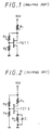
self-bias system shown in FIG. 1 of the accompanying drawings.
As shown in FIG. 1, because the source portion of an FET1 is
directly grounded, this voltage feedback type self-bias system
has an advantage that a distortion of a signal is small but
has a disadvantage that the bias is not stable. Therefore, it
is customary that a current feedback type self-bias system in
which a resistor R7 is connected to the source portion of an
FET2 as shown in FIG. 2 is used. The bias system shown in
FIGS. 1 and 2 are DC equivalent circuits.
However, the resistor R7 is connected to the source
portion of the FET2, a gain of the signal amplified by the
FET2 is reduced. Therefore, the current feedback type self-bias
system includes a bypass capacitor C1 in order to
increase the gain of the amplified signal. It is sufficient
that a capacitance of the bypass capacitor C1 is about several
10s of picofarads when the MMIC is operated at a frequency of,
for example, about 2GHz in the transmission system.
Accordingly, there is substantially no difference in gain as
compared with the case that the source portion is directly
grounded irrespective of a bias stability.
When the current feedback type self-bias system is
used as the MMIC used in a high frequency signal reception
system, however, in order to improve a three-order cross
modulation distortion output that is particularly an important
problem, it is not sufficient that the capacity of the bypass
capacitor C1 is about several 10s of picofarads. To obtain a
characteristic that is substantially the same as that obtained
when the source portion of the FET2 is directly grounded, the
capacitance of the bypass capacitor C1 must be increased more
than several 100s of picofarads. Incidentally, the three-order
cross modulation distortion output will be described
fully later on.
When a bypass capacitor having a capacitance os
several 100s of picofarads or more is formed on the MMIC by an
MIM (metal insulator metal) structure, if a 0.2µm-thick
silicon nitride film having a specific inductive capacity of 7
is used as an insulating film, then an area of the bypass
capacitor C1 becomes several squares millimeters, which is not-practical.
When the bypass capacitor C1 is connected thereto
from the outside as a chip assembly part, the number of
package pins is increased. In addition, when the bypass
capacitor C1 is applied to a high frequency of about 2GHz,
there are many restrictions that an inductance of a bonding
wire cannot be neglected.
Further, when the resistor R7 is connected to the
source portion of the FET2, a potential difference between the
drain portion and the source portion is reduced by an amount
corresponding to a voltage drop across the resistor R7 so that
an output dynamic range of the FET2 is decreased. There is
then the problem that a power consumption is increased by the
resistor R7. These problems become remarkably serious when
the FET is operated at low voltage or with a large amplitude.
As earlier noted, the MMIC generally uses the GaAs
MESFET. In the MESFET that is placed in the enhancement mode,
a diffusion potential d is about 0.6V at most and therefore
the threshold voltage VTH cannot be made high. Accordingly,
when the MESFET is used, an operation margin for the
fluctuation of the threshold voltage VTH is small so that a
negative power supply is required. Hence, the MESFET cannot
be driven by a single power supply of low voltage.
The device per se will be described next. The GaAs
semiconductor is inferior in crystalinity as compared with the
silicon semiconductor and a semiconductor is formed of two
elements. Therefore, the control of the ion implantation
process of impurity is difficult. Also, because the semi-insulating
substrate is used, an electric charge distribution
due to a piezo-electric effect is fluctuated. Thus, in the
existing manufacturing process of the GaAs FET, the threshold
value Vth of the FET cannot be controlled with high accuracy
substantially. A value of a mutual conductance gm of the GaAs
FET is as large as about several 100s ms/mm and therefore a
drain current Id is fluctuated considerably with the
fluctuation of the threshold voltage Vth. Since the gain of
the MMIC depends upon the drain current Id, the drain current
must be made constant, which requires the MMIC to have the
bias stabilizing circuit therein.
In order to supply the fixed bias voltage to the
MMIC, the bias voltage must be adjusted when the MMIC is
assembled into various equipments. Furthermore, since the
threshold voltage Vth has a temperature dependence and has a
large mutual conductance gm, the threshold voltage Vth is
easily fluctuated by about 0.1V in a temperature range of, for
example, 100°C. As a result, the FET characteristic is
considerably fluctuated with the change of temperature, which
requires a temperature compensation circuit formed of a
thermistor or the like.
Therefore, in the MMIC formed of the GaAs FET, the
bias must be stabilized and the adjustment of the bias must be
removed.
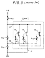
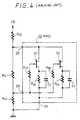
An example of the related-art bias circuit formed of
the MMIC of the enhancement type GaAs FET will be described
with reference to FIG. 3. As shown in FIG. 3, an MMIC 10 is
formed of a plurality of FETs (N-channel type FETs) 17, 18, 19
that are connected at their drains and sources in parallel to
one another from a DC standpoint. The drains of the
respective FETs 17, 18, 19 are commonly connected to lead out
a drain terminal 1D, and the sources thereof are commonly
connected through gate resistors R14, R15, R16 to lead out a
gate terminal 1G. In this example, the FETs 17, 18, 19 are
each MES (metal-semiconductor) - FETs.
The bias circuit will be described next. This bias
circuit is a voltage feedback self-bias type circuit. A
series circuit of resistors R11, R12, R13 sequentially
connected is interposed between a power supply +B and the
ground. A junction between the resistors R11 and R12 is
connected to the drain terminal 1D. A junction between the
resistors R12 and R13 is connected to the gate terminal 1G,
and the source terminal 1S is grounded.
Because the sources of the FETs 17, 18, 19 are
directly grounded, the bias circuit of this voltage feedback
type self-bias system has an advantage that a signal
distortion is small but has a defect that a bias stability is
low.
There is proposed a bias circuit of a current
feedback type self-bias system in which bias resistors R24,
R26 are interposed between the sources of FETs 21 and 22 and
the ground in addition to the circuit arrangement shown in
FIG. 3 as shown in FIG. 4. In FIG. 4, reference symbols C2,
C3 represent bias capacitors respectively connected to the
bias resistors R24, R26 in parallel.
It is sufficient that the capacitance of each of the
bypass capacitors C2, C3 is about several 10s of picofarads
when the signal frequency is 2GHz irrespective of the cross
modulation distortion characteristic. Also, irrespective of
the bias stability, the increase of the gain of the FETs 21,
22 is very small as compared with the case that the source of
the FETs 21, 22 are directly grounded.
When the bias circuit of the current feedback type
self-bias system is provided on the FETs in the MMIC used in
the high frequency signal reception system, the capacitance of
the above-mentioned bypass capacitor must be selected to be
more than several 100s of picofarads in order to improve a
three-order cross modulation distortion output. In this case,
it is very difficult to incorporate such bypass capacitor
within the MMIC. Moreover, if such bypass capacitor is
connected to the MMIC from the outside, then it is unavoidable
that the number of terminal pins in the MMIC is increased to
that extent. In this connection, when the capacitor whose
capacitance is 100pF is formed into the MMIC, if the capacitor
is sandwiched by a metal film of an insulating layer (0.2µm-thick
silicon nitride film having a specific inductive
capacitance of 7), its area becomes several squares
millimeters, which is not practical. Also, when the signal
frequency becomes 2GHz, an inductance of the bonding wire
cannot be neglected.
Further, when the bias resistor is connected to the
source of the FET, a voltage between the drain and the source
is lowered by an amount corresponding to the voltage drop
across such resistor. As a consequence, a dynamic range of
the FET is reduced, and the power consumption of that resistor
becomes useless.
The assignee of the present application has
previously proposed an FET bias stabilizing circuit (not laid-open
when the present application is filed) formed of a
compound semiconductor in which a bias stability is high, an
operation margin against a fluctuation of a threshold voltage
Vth is large and which can be driven by a single low voltage
power supply.
An example of a prior-art bias stabilizing circuit
for the MMIC made of a GaAs enhancement type FET will be
described with reference to FIG. 5. Similarly as described
above, in an MMIC 30, a plurality of FETs (N-channel type
FETs) 31, 32, 33 are connected in parallel to one another at
their drains and sources from a DC standpoint. The drains of
the FETs 31, 32, 33 are commonly connected to lead out a drain
terminal 3D, and sources thereof are commonly connected to
lead out a source terminal 3S. Also, the gates of the FETs
31, 32, 33 are commonly connected through gate resistors R33,
R34, R35 to lead out a gate terminal 3G. In FIG. 5, each of
the FETs is a J (junction type) - FET or MES-FET.
The bias circuit will be described next. This bias
circuit is a current-mirror type bias circuit. As shown in
FIG. 5, between the power supply +B and the ground, there is
connected a series circuit formed of a resistors R31, R32, and
drain and source of an FET (N-channel type FET) 34 whose drain
and gate are directly coupled. A junction between the
resistors R31, R32 is connected to the drain terminal 3D, the
drain (gate) of the FET 34 is connected to the gate terminal
3G, and the source terminal 3S is grounded. The FET 34 is the
J-FET or MES-FET and is formed of the same kind of the FETs
31, 32, 33.
An example of a practical circuit of the example of
the prior art shown in FIG. 5 will be described with reference
to FIG. 6. As shown in FIG. 6, a signal input terminal Tin is
led out from the gates of FETs 41, 42 of the MMIC through a
coupling capacitor C6, and a signal output terminal Tout is
led out from the drains of the FETs 41, 42 through a coupling
capacitor C7. Drains of the FETs 41, 42 are connected through
coils (inductances) L1, L2 serving as loads to a drain
terminal 4D, and the drain terminal 4D is grounded through a
capacitor C8 which presents a low impedance relative to a
signal. A gate terminal 4G is grounded through a capacitor C5
which presents a low impedance relative to a signal.
According to the example of such prior art as shown
in FIG. 6, when the temperatures of the FETs 41, 42, 43 rise,
the threshold values Vth thereof are lowered respectively so
that, even if a DC drain current of the FET 43 is increased
(or decreased), a DC drain voltage of the FET 43 is lowered
(increased), thereby suppressing the DC drain current from
being increased (decreased). As a consequence, the DC drain
current is not changed at all, whereby DC drain currents of
the FETs 41, 42, i.e., bias drain currents are not changed.
Further, when the FETs 41, 42 and 43 are J-FETs, the diffusion
potential D is about 1.2V and sufficiently high as compared
with that of the MES-FET. Therefore, tolerance fluctuation
widths of the threshold voltages Vth of the FETs 41, 42, 43
are wide and this bias circuit can be operated by a single low
voltage power supply.
Incidentally, the power supply +B and the drain
terminal 4D may be connected together directly. If the
resistor R41 is interposed between the power supply +B and the
drain terminal 4D, then a bias stability can be increased.
FIG. 7 shows a relationship between a characteristic
of the drain current (mA) versus threshold voltages Vth (V) of
the FETs 41, 42 in the examples of the prior art shown in
FIGS. 5 and 6 in comparison with that of the example of the
prior art shown in FIG. 4. In FIG. 7, a solid line shows a
characteristic measured when the resistor R41 in the examples
of the prior art shown in FIGS. 5 and 6 is removed. A broken
line in FIG. 7 shows a characteristic measured when the above-mentioned
resistor R41 is provided. A one-dot chain line in
FIG. 7 shows characteristic measured in the case of the prior
art example of FIG. 4.
As described above the bias stabilizing circuits of
the GaAs semiconductor FETs according to the prior-art
examples shown in FIGS. 5 and 6 have the advantage such that
the bias stability is high, the tolerance fluctuation width of
the threshold voltage Vth is wide and can be driven by the
single low voltage power supply.
When the bias stabilizing circuit of the GaAs
semiconductor FET according to the prior-art example use the
single low voltage power supply of about 3V, if a
fluctuation ratio of the DC drain current is suppressed
in a range of from ± 10 %, when the tolerance
fluctuation width of the threshold voltage Vth falls in
a range of from ± 0.1 to 5V at best. Therefore, it is
impossible to suppress the tolerance fluctuation width
of the threshold voltage Vth so that width from an IC
manufacturing technology standpoint.
OBJECTS AND SUMMARY OF THE INVENTION
Therefore, it is an object of the present
invention to provide an MMIC having a self-bias circuit
in which a bias stability is high, a bias capacitor can
be removed and in which the occurrence of a distortion
is small.
It is another object of the present invention to
provide an MMIC having a self-bias circuit in which an
operation margin for a fluctuation of a threshold
voltage is large and which can be driven by a single
low voltage power supply.
It is a further object of the present invention to
provide a monolithic microwave semiconductor integrated
circuit apparatus which can generate a bias voltage
near a threshold voltage of an FET.
To solve these objects the present invention
provides a microwave semiconductor integrated circuit
as specified in claim 1.
Preferred embodiments of the invention are
described in the subclaims.
In accordance with an aspect of the present
invention, there is provided a microwave semiconductor
integrated circuit for generating a bias voltage that
is applied to an active circuit element. This microwave
semiconductor integrated circuit comprises a field
effect transistor whose source is grounded and whose
gate and drain are connected commonly, a negative
element for applying a power source voltage to a gate-drain
common connection point of the field effect
transistor, and a high impedance element for supplying
a potential at the gate-drain common connection point
of the field effect transistor to the active circuit
element as a bias voltage.
A monolithic microwave semiconductor integrated
circuit includes a bias stabilizing circuit of a
current mirror type formed of a bias control transistor
formed of an enhancement mode compound semiconductor
field effect transistor and a biased transistor formed
of an enhancement mode compound semiconductor field
effect transistor.
A monolithic microwave semiconductor integrated
circuit includes a bias stabilizing circuit of a
current mirror type formed of a bias control transistor
formed of an enhancement mode junction field effect
transistor and a biased transistor formed of an
enhancement mode junction field effect transistor.
A bias stabilizing circuit for a field effect
transistor formed of a compound semiconductor which is
comprised of a bias circuit in which one output
electrode of the bipolar transistor which is applied at
its base with a bias voltage is connected through a
first resistor to a power supply and the other output
electrode is grounded through a second resistor, and a
field effect transistor formed of a compound
semiconductor biased by the bias circuit, wherein one
output electrode of the bipolar transistor is connected
to one output electrode of the field effect transistor
and the other output electrode of the bipolar
transistor is connected to the gate of the field effect
transistor. This arrangement enables a bias stabilizing
circuit for a field effect transistor formed of a
compound semiconductor in which a bias stability is
high a tolerance fluctuation width of a threshold
voltage is sufficiently wide and which can be operated
by a single low voltage power supply.
The above and other objects, features, and
advantages of the present invention will become
apparent from the following detailed description of
illustrative embodiments thereof to be read in
conjunction with the accompanying drawings, in which
like reference numerals are used to identify the same
or similar parts in the several views.
BRIEF DESCRIPTION OF THE DRAWINGS
Fig. 1 is a schematic diagram showing an example
of an FET bias circuit according to the related art;
Fig. 2 is a schematic diagram showing other
example of the FET bias circuit according to the
related art;
Fig. 3 to 5 are schematic diagrams showing further
examples of the FET bias circuits according to the
related art, respectively;
Fig. 6 is a schematic diagram showing an example
of the prior art-amplifying circuit using the FET bias
circuit
shown in FIG. 5;
FIG. 7 is a graph showing a relationship between-an
operation voltage and an operation current of the amplifying
circuit shown in FIG. 6;
FIG. 8 is a schematic diagram showing a first
embodiment of an FET bias circuit according to the present
invention;
FIG. 9 is a schematic diagram showing a second
embodiment of an amplifying circuit using the FET bias circuit
shown in FIG. 8;
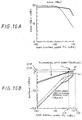
FIGS. 10A and 10B are graphs showing measured
results of a gain and a distortion of the amplifying circuit
shown in FIG. 9, respectively;
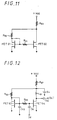
FIG. 11 is a schematic diagram showing a third
embodiment of the FET bias circuit according to the present
invention;
FIG. 12 is a schematic diagram showing a fourth
embodiment of an amplifying circuit using the FET bias circuit
shown in FIG. 11 according to the present invention;
FIG. 13 is a graph showing a relationship between a
threshold voltage and a drain current of the amplifying
circuit shown in FIG. 12;
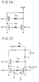
FIGS. 14 and 15 are schematic diagrams showing a
fifth embodiment of the FET bias circuit according to the
present invention, and an amplifying circuit using such FET
bias circuit, respectively;
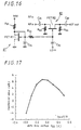
FIG. 16 is a schematic diagram showing a sixth
embodiment of the amplifying circuit according to the present
invention;
FIGS. 17, 18 and 19 are respectively graphs showing
a relationship among a gate bias voltage, a conversion gain, a
drain current and a threshold voltage of the amplifying
circuit shown in FIG. 16;
FIG. 20 is a schematic diagram showing a seventh
embodiment of a mixer circuit according to the present
invention;
FIG. 21 is a schematic diagram showing an eighth
embodiments of the FET bias circuit;
FIG. 22 is a schematic diagram showing a ninth
embodiment of the amplifying circuit using the bias circuit
shown in FIG. 21;
FIGS. 23 and 24 are a bias characteristic graph of
the amplifying circuit shown in FIG. 22 and a diagram showing
measured values, respectively;
FIG. 25 is a schematic diagram showing a tenth
embodiment of the FET bias circuit;
and
FIG. 26 is a schematic diagram showing an eleventh
embodiment of the FET bias circuit.
DETAILED DESCRIPTIO OF THE PREFERRED EMBODIMENTS
Embodiments of the present invention will
hereinafter be described with reference to the drawings.
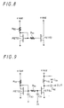
FIG. 8 shows an equivalent circuit diagram of the
first embodiment of the bias circuit of the MMIC according to
the present invention. As shown in FIG. 8, the MMIC of the
first embodiment includes a current mirror type bias
stabilizing circuit formed of a bias control transistor FET 51
and a biased transistor FET 52.
In FIG. 8, each of the bias control transistor FET
51 and the biased transistor FET 52 is formed of a
semiconductor field effect transistor of an enhancement mode,
and more practically, each of them is formed of MESFET or JFET
formed of III/V-compound semiconductor. A source portion of
the biased transistor FET 52 is grounded directly. Also, the
bias control transistor FET 51 is an element used to stabilize
the bias voltage. Further, the biased transistor FET 52 is an
element that is operated as an amplifier, a mixer or an
oscillator in actual practice.
A gate portion of the biased transistor FET 52 and
the gate portion of the bias control transistor FET 51 are
connected through a first resistor R51. A drain portion of
the biased transistor FET 52 is connected to a power supply
+Vdd. The source portion of the biased transistor FET 52 is
grounded directly as set forth above. A gate portion of the
bias control transistor FET 51 is short-circuited to the drain
portion of the bias control transistor FET 51. The drain
portion of the bias control transistor FET 51 is connected
through a second resistor R52 to the power supply +Vdd. The
source portion of the bias control transistor FET 51 is
grounded as described above.
FIG. 9 shows a circuit arrangement of a second
embodiment of the MMIC bias circuit according to the present
invention provided when a high frequency characteristic is
taken into consideration. As shown in FIG. 9, a signal input
terminal IN is provided between a first resistor R54 through a
capacitor C51. A signal is input to the biased transistor FET
54 from this signal input terminal IN. A signal output
terminal OUT is connected to a drain portion of the biased
transistor FET 54 through a capacitor C52, and a signal is
output from this signal output terminal OUT.
As shown in FIG. 9, it is preferable that a grounded
capacitor C53 is interposed between the first resistor R54 and
the gate portion of a bias control transistor FET 53. The
first resistor R54 and the capacitor C53 constitute a low-pass
filter. It is preferable that this low-pass filter is
connected between the input terminal IN and the gate portion
of the bias control transistor FET 53. Thus, a high frequency
circuit portion formed of the biased transistor FET 54 and the
bias circuit portion formed of the bias control transistor FET
53 can be insulated from each other electrically. More
specifically, a potential of the gate portion of the bias
control transistor FET 53 can be prevented from being changed
due to the influence of a signal from the signal input
terminal IN. Also, the gate portion of the bias control
transistor FET 53 can be prevented from being affected by an
extraneous noise. In the microwave band, it is sufficient
that a resistance value of the first resistor R54 is selected
to be several 10s of kilo ohms and a capacitance of the
capacitor C53 is selected to be several picofarads.
The bias control transistor FET 53 and the biased
transistor FET 54 may be connected to a single power supply or
a plurality of power supplies including a negative power
supply.
Operation of this current mirror type bias
stabilizing circuit has already been described and therefore
need not be described in detail herein.
A difference between high frequency characteristics
of the MMIC including the current mirror type bias stabilizing
circuit of the present invention and the conventional MMIC
including the current feedback self-bias system bias
stabilizing circuit mainly appears in a distortion
characteristic. FIGS. 10A and 10B show simulated results of
these high frequency characteristics. Incidentally, a
capacity of the bypass capacitor C1 of the conventional MMIC
was selected to be 20pF. Upon simulation, it is assumed that
an MMIC is formed of biased transistors of two stages
connected in cascade. FIG. 10A shows a gain Ga (output
voltage/input voltage) of the 2GHz band amplifier. FIG. 10B
shows simulated results in which a fundamental output Poutfund
provided when two close waves are input and a three-order
cross modulation distortion output PoutIM are plotted relative
to an input electric power Pin, respectively. Further, FIG.
10B shows a value IIP which is an input equivalent to the
intercept point IP and a value OIP which is an output
equivalent thereto in the respective systems. In FIGS. 10A,
10B, solid lines represent simulated results obtained in the
case of the MMIC of the present invention, and broken lines
represent simulated results obtained in the case of the
conventional MMIC including the bias stabilizing circuit of
the current feedback self-bias type.
When a signal having two close frequencies f1 and f2
of the same level (a value of (f1-f2)/f1 is about 0.1%) is
input to the MMIC, there are output not only a signal
(fundamental wave) having the frequencies f1, f2 but also a
signal having secondary harmonic waves 2f1 and 2f2. Further,
a three-order cross modulation distortion having frequencies
(2f1-f2) or (2f2-f1) is output. Poutfund depicts an output of
the fundamental output having the frequencies f1, f2. Also,
PoutIM depicts a three-order cross modulation distortion
having frequencies of (2f1-f2) or (2f2-f1). When the input
voltage Pin is changed, a ratio in which PoutIM is changed is
three times the ratio in which Poutfund is changed.
As shown in FIG. 10B, Poutfund and PoutIM are
saturated when the input electric power Pin is increased. In
an input electric power P in which a linear characteristic is
established, a tangent L1 of Poutfund and a tangent L2 of
PoutIM are calculated. In this case, a point in which the
above-mentioned two tangents L1 and L2 cross each other is
referred to as an intercept point IP. IIP represents a value
in which the intercept point IP is transformed into input, and
OIP represents a value in which the intercept point IP is
transformed into output. If the values of IIP and OIP are
larger, then the three-order cross modulation distortion
becomes smaller.
As is clear from FIGS. 10A and 10B, the MMIC of the
present invention and the conventional MMIC are substantially
the same with respect to the gain Ga but they have a
difference of about 7dB therebetween with respect to the IIP
and OIP which are indexes of distortion characteristic. More
specifically, the MMIC of the present invention in which the
resistor is not inserted into the source portion of the biased
transistor FET 54 has a better distortion characteristic.
Results similar to these simulated results were confirmed in
the MMIC amplifier that was manufactured in actual practice.
A third embodiment of the present invention will be
described next. As shown in FIG. 11, a drain portion of a
biased transistor FET 62 and a second resistor R62 are
connected to a power supply +Vdd through a resistor R63,
thereby further increasing a stability of the bias stabilizing
circuit.
FIG. 13 shows a fluctuation of a drain current Id2
of the biased transistor FET 62 against the fluctuation of a
threshold voltage VTH2, i.e., bias stability. A solid line in
FIG. 13 shows a measured fluctuation obtained by the MMIC
having the bias stabilizing circuit according to the first
embodiment of the present invention, and a dashed line in FIG.
13 shows a measured fluctuation obtained by the MMIC having
the bias stabilizing circuit according to the present
invention shown in FIG. 11 (i.e., the resistor R63 is
inserted). Also, a one-dot chain line in FIG. 13 shows a
measured fluctuation obtained by the MMIC using the
conventional current feedback self-bias type. Study of FIG.
13 reveals that the MMIC according to the present invention
has a bias stability substantially the same as that of the
conventional current feedback self-bias type. In addition, in
the third embodiment in which the resistor R63 is inserted in
the current mirror type bias stabilizing circuit is increased
in bias stability as compared with the embodiment of the first
embodiment.
A fourth embodiment of the present invention will be
described below. A circuit arrangement in which the DC
equivalent circuit and the high frequency characteristic of
the bias circuit of the MMIC according to the fourth
embodiment of the present invention can be made substantially
similar to those of the first or third embodiment. More
specifically, the MMIC according to the fourth embodiment of
the present invention also includes a bias stabilizing circuit
of a current mirror type formed of a bias control transistor
FET 63 and a biased transistor FET 64, similarly to the first
or third embodiment.
The fourth embodiment is different from the first
and third embodiments in that the bias control transistor FET
63 and the biased transistor FET 64 must be formed of
enhancement mode type junction field effect transistors
(JFETs). It is preferable that the JFET is formed of III/V-compound
semiconductor such as GaAs or the like. Further, a
drain portion of the bias control transistor FET 63 is
connected through a second resistor R66 to a power supply
(single power supply) to which a drain portion of the biased
transistor FET 64 is connected.
More specifically, the gate portion of the biased
transistor FET 64 is connected through a first resistor R65 to
the gate portion of the bias control transistor FET 63. The
drain portion of the biased transistor FET 64 is connected to
the power supply. A source portion of the biased transistor
FET 64 is grounded directly. A gate portion of the bias
control transistor FET 63 is short-circuited to the drain
portion of the bias control transistor FET 63. The drain
portion of the bias control transistor FET 63 is connected to
one end of a second resistor R66, and the other end of the
second resistor R66 is connected to the power supply to which
the drain portion of the biased transistor FET 64 is
connected. A source portion of the bias control transistor
FET 63 is grounded.
As earlier noted in the MESFET of the enhancement
mode type, the diffusion potential D is about 0.6V at most
and the threshold voltage VTH cannot be increased. Therefore,
when the MESFET is used, it is frequently observed that the
operation margin for the fluctuation of the threshold voltage
VTH is small, requiring the negative power supply. As a
consequence, the MESFET cannot be driven by a single power
supply of low voltage substantially. If the MESFET is
operated by a single power supply, a resistor must be
connected to the source portion of the biased transistor FET
64 to supply an offset voltage. In this case, there occurs
the problem that had been described in connection with the
current feedback self-bias system.
However, the diffusion potential D of the JFET is
about 1.2V and is sufficiently high as compared with that of
the MESFET. Therefore, the operation margin for the
fluctuations (fluctuations of about ±0.2V) of the threshold
voltages VTH1 and VTH2 are large and the negative-power supply
is not necessary. Thus, the MMIC can be operated with the
single low voltage power supply.
Operation of the bias stabilizing circuit of the
current mirror type according to the fourth embodiment of the
present invention is the same as described herein before and
therefore need not be described in detail.
A fifth embodiment of the present invention is a
modification of the fourth embodiment. While the resistor R66
is connected between the drain portion of the bias control
transistor FET 63 and the power supply in the fourth
embodiment, according to the fifth embodiment, a second bias
control transistor FET 73 formed of an enhancement mode type
junction field effect transistor is connected instead of the
resistor R66 as shown in the DC equivalent circuit of FIG. 14
and in consideration of a high frequency characteristic shown
in FIG. 15.
To be more concrete, a gate portion of a biased
transistor FET 72 is connected through a first resistor R71 to
a gate portion of the bias control transistor FET 71, and a
drain portio of the biased transistor FET 72 is connected to
the power supply and its source portion is grounded directly.
A gate portion of the bias control transistor FET 71 is short-circuited
to the drain portion of the bias control transistor
FET 71. The drain portion of the bias control transistor FET
71 is connected to a source portion of a second bias control
FET 73, and the source portion of the bias control transistor
FET 71 is grounded. A gate portion of the second bias control
transistor FET 73 is connected to the drain portion of the
biased transistor FET 72 by way of the second resistor R72. A
drain portion of the second bias control transistor FET 73 is
connected to the power supply to which the drain portion of
the biased transistor FET 72 is connected.
Operation of the bias stabilizing circuit of this
embodiment will be described in association with the
equivalent circuit of the bias stabilizing circuit of the
current mirror type shown in FIG. 14 and with reference to
FIG. 15. When temperatures of a bias control transistor FET
74 and a biased transistor FET 75 rise, the threshold voltages
VTH1 and VTH2 of the bias control transistor FET 74 and the
biased transistor FET 75 are lowered so that drain currents
Id1, Id2 flowing through the bias control transistor FET 74
and the biased transistor FET 75 are increased. As a
consequence, a voltage drop across a second resistor R74
becomes large and the gate voltage of a second bias control
transistor FET 76 is lowered, thereby a resistance value of
the second bias control transistor FET 76 being increased.
Consequently, a potential Vds1 between the drain portion and
the source portion of the bias control transistor FET 74 is
lowered. Since the drain portion and the gate portion of the
bias control transistor FET 74 are short-circuited as
described above, a potential Vgs1 between the gate portion and
the source portion of the bias control transistor FET 74 is
lowered as the potential Vds1 is lowered. As a consequence,
the feedback is effected so as to decrease the drain current
Id1 flowing the bias circuit, thereby suppressing the
fluctuation of the drain current Id1.
The threshold voltage VTH1 of the bias control
transistor FET 74 and the threshold voltage VTH2 of the biased
transistor FET 75 can be regarded as being substantially the
same. Since the gate portion of the bias control transistor
FET 74 and the gate portion of the biased transistor FET 75
are connected together via a first resistor R73, the gate
portion of the biased transistor FET 75 is applied with a bias
voltage that depends on the change of the potential Vgs1 of
the bias transistor FET 74. Therefore, the drain current Id2
flowing the biased transistor FET 75 is kept substantially
constant regardless of the fluctuation of the threshold
voltage VTH2.
With the above-mentioned arrangement, the bias can
be stabilized more as compared with the fourth embodiment.
While the preferred embodiments have been described
so far, the present invention is not limited to those
embodiments. In the practical circuit arrangement, resistors
must be inserted into a variety of positions of the circuit in
order to adjust the voltage. Also, in order to cut off the
high frequency, capacitors must be inserted into various
positions of the circuit, which are not shown in the figures.
Since the MMIC according to the first and second
modes of the present invention includes the bias stabilizing
circuit of the current mirror type, the resistor need not be
connected to the source portion of the biased transistor in
order to stabilize the bias. Therefore, the bypass capacitor
need not be provided and in addition, the distortion can be
reduced, the output dynamic range can be widened, and the low
power consumption can be achieved. Further, a bias stability
substantially the same as that provided by the current
feedback self-bias type can be obtained, and the bias need not
be adjusted.
A sixth embodiment of the present invention will
hereinafter be described with reference to the drawings.
FIG. 16 is a diagram showing a circuit arrangement
of the sixth embodiment of the present invention that is
applied to an example of a mixer circuit 82.
As shown in FIG. 16, a bias circuit 81 that
generates a bias voltage is formed by using an enhancement
mode GaAs FET 81. A source of the FET 81 is grounded, and the
gate and the drain thereof are commonly coupled. A capacitor
C84 is connected between the gate of the FET 81 and the
ground. A common connection point between the gate and the
drain of the FET 81 is applied with a power supply voltage Vdd
through a load resistor R81.
A potential at the gate-drain common connection
point of the FET 81 is supplied to an FET 82 which is an
active circuit element that constructs a mixer circuit 82
through a resistor R82 serving as a high impedance element as
a gate bias voltage Vgg.
In the mixer circuit 82, an RF signal is input
through a capacitor C81 to the drain (or source) of an FET 82.
The gate bias voltage Vgg supplied from the bias circuit 81 is
supplied to the gate of the FET 82. Also, a local oscillation
signal (LO signal) is input to the gate of the FET 82 through
a capacitor C82. A drain and a source of the FET 82 are
respectively grounded via resistors R83 and R84.
An IF (intermediate frequency) signal that results
from mixing the RF signal and the local oscillation signal by
the FET 82 is output from the source (or drain) of the FET 82
through a capacitor C83.
Incidentally, the local oscillation signal applied
to the gate of the FET 82 is cut off by a low-pass filter
formed of a resistor R82 and the capacitor C84 so that the
local oscillation signal can be prevented from affecting the
bias circuit 81.
As is clear from a characteristic diagram of FIG.
17, in the mixer circuit 82 thus arranged, the mixer
conversion gain considerably depends upon the gate bias
voltage Vgg and a voltage that can provide a maximum conversion
gain is near the threshold voltage Vth.
A gate bias voltage dependence of conversion gain of
an evaluation sample whose threshold voltage Vth is about 0.1V
was measured.
Since the bias circuit 81 and the mixer circuit 82
are formed of integrated circuits, although the threshold
voltages Vth of the FETs 81, 82 are fluctuated with the
process, relative values thereof are not fluctuated and can be
regarded as substantially the same.
In order to approximate the gate bias voltage Vgg of
the FET 82 to the threshold voltage Vth such that a maximum
gain of the mixer circuit 82 is obtained, in the bias circuit
81, the on-resistance value Ron of the FET 81 must be reduced
sufficiently.
As an example of achieving this object, it is
sufficient that a gate width wg of the FET 81 is increased
sufficiently.
More specifically, in a characteristic diagram of
FIG. 18, as the gate width wg of the FET 81 is increased, a
curve of Vgg -Ig (drain current) shown by a solid curve rises.
Also, as the load resistor R81 is increased, an inclination of
a straight line of Vdd/R81 shown by a one-dot chain line
becomes gentle.
In this characteristic, a crossing point (Mark x in
FIG. 18) between the Vgg -Ig curve and the Vdd/R81 straight line
represents a bias points (gate bias voltage Vgg). When the
gate width wg of the FET 81 is large and the load resistor R81
is large, the gate bias voltage Vgg approaches the threshold
voltage Vth.
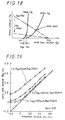
FIG. 19 shows a dependence characteristic of the
threshold voltage Vth of the gate bias voltage Vgg relative to
the gate width wg and the load resistor R81 obtained when the
power supply voltage Vdd is set to 3V, for example.
In this characteristic graph of FIG. 19, a one-dot
chain line curve (a) represents a characteristic obtained when
wg = 20 µm and R81 = 10 KΩ. A two-dot chain line curve (b)
represents a characteristic obtained when wg = 20 µm and R81 =
100 KΩ. A broken line curve (c) represents a characteristic
obtained when wg = 200 µm and R81 = 100 KΩ. Study of FIG. 19
reveals that, as the gate width wg and the load resistor are
both large, the gate bias voltage Vgg approaches the threshold
voltage Vth inasmuch as the threshold voltage Vth that is in
the enhancement mode falls within a positive range.
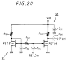
FIG. 20 shows a mixer circuit 93 which is a seventh
embodiment of the present invention.
In the mixer circuit 93 according to this
embodiment, the RF signal and the local oscillation signal are
both supplied through a capacitor C94 to the gate of an FET
93. A source of the FET 93 is grounded and the drain thereof
is applied with the power supply voltage Vdd through a resistor
R93.
Then, an IF signal that results from mixing the RF
signal and the local oscillation signal is output from the
drain the FET 93 through a capacitor C95.
A bias circuit 91 is constructed in exactly the same
manner as that in the aforesaid embodiment. Accordingly, by
setting the gate width wg of an FET 91 and a load resistor R91
to be sufficiently large, a voltage that is close to the
threshold voltage Vth can be set as the gate bias voltage Vgg
of FET 93 of the mixer circuit 93 similarly to the above-mentioned
embodiments.
While in the above embodiments the bias voltage
generated in the bias circuit is applied to the mixer circuit
as described above, the present invention is not limited
thereto and can be applied to the whole of circuits that
require the gate bias voltage near the threshold voltage Vth
in the microwave semiconductor device using the enhancement
mode GaAs FET.
As described above, according to the present
invention, since there is used the FET whose source is
grounded and whose gate and source are connected commonly, the
power supply voltage is applied through the load element to a
common connection point of the gate and the drain of this FET,
and the potential at this common connection point is supplied
to the active circuit element through a high impedance element
as the bias voltage, there can be generated a bias voltage
that is close to the threshold voltage Vth of FET by
sufficiently increasing the gate width of the FET and the load
resistor.
An eighth embodiment will
be described below.
A circuit configuration of the eighth embodiment
will be described below with reference
to FIG. 21. As shown in FIG. 21, an MMIC 100 is formed of a
plurality of FETs (N-channel FETs in this embodiment) 102,
103, ... 104 whose drains and sources are each connected in
parallel from a DC standpoint. The drains of the respective
FETs 102, 103, ... 104 are commonly connected to lead out a
drain terminal 100D, and the sources thereof are commonly
connected to lead out a source terminal 100S. The gates
thereof are commonly connected through gate resistors 105,
106, ... 107 to lead out a gate terminal 100G. Incidentally,
the FETs 102, 103, ... 104 are each formed of enhancement mode
type J-FETs.
The bias circuit will be described next. As shown
in FIG. 21, there is provided a PNP-type bipolar transistor
Q100. A series circuit of resistors R101 and R102 is
connected between the power supply +B and the ground. A
junction between the resistors R101 and R102 is connected to
the base of the transistor Q100, whereby a fixed bias voltage
is applied to the base thereof. The emitter of the transistor
Q100 is connected through a resistor R103 to the power supply
+B, and the collector thereof is grounded through a resistor
R104. The emitter of the transistor Q100 is connected to the
drain terminal 100D, and the collector thereof is connected to
the gate terminal 100G. The source terminal 100S is grounded.
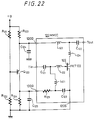
FIG. 22 shows a ninth embodiment.
As shown in FIG. 22, there is provided a signal
input terminal Tin which is connected through a matching
circuit formed of a capacitor C121 and coils (inductances)
L121, L122 to the gate of an FET 122. This matching circuit
causes an input impedance to become 50Ω as seen from the input
terminal Tin. The input terminal Tin is sequentially
connected through the capacitor C121 and the coil L122 to the
gate of the FET 122. A junction between the capacitor C121
and coil L122 is connected to one end of the coil L121, and
the other end thereof is grounded through a capacitor C123
which presents a low impedance relative to a signal. A gate
terminal 120G is grounded through a capacitor C125 that
presents a low impedance relative to the signal. A drain of
the FET 122 is connected to a drain terminal 120D through a
series circuit of coils (inductances) L123, L124. A junction
between the coils L123 and L124 is connected through a
capacitor C122 to a signal output terminal Tout. The coils
L123, L124 and the capacitor C122 constitute a matching
circuit which makes an output impedance to be 50Ω as seen from
the signal output terminal Tout.
A mechanism of the bias circuit (bias stabilizing
circuit) according to the ninth embodiment
will be described below. A collector current Ic of
the bipolar transistor Q120 is expressed as;
Ic = [{R121/(R121+R122)V+-Vbe}
- ReIdd]/{R123+R121·R122/(R121+R122)/hfe}
In the equation (1), R121 and R122 represent
resistance values of the resistors R121, R122, V+ represents
the voltage of the power supply +B, Vbe represents the base-emitter
voltage of the transistor Q120, R123 represents the
resistance value of the resistor R123, Idd represents a total
sum of drain currents flowing through the drain of each of the
FETs 122 from the drain terminal 120D, and hfe represents an
emitter ground current amplification factor of the transistor
Q120. Incidentally, a current that flows from the gate
terminal 120G to the gate of the FET 122 is very small and
therefore can be neglected.
A DC voltage Vgg at the gate terminal is expressed by
the following equation:
Vgg = R124Ic
From the above-mentioned equations (1) and (2), the
total sum of the DC drain currents that flow from the drain
terminal 120D to the drain of the FET 122 is expressed by the
following equation:
Idd = -aVgg + b
The coefficients a and b are expressed by the
following equations:
a = {R123 + R121·R122/(R121+R122)/hfe}/R124·R123 b = {R121·V+/(R121+R122) - Vbe}/R123
Incidentally, a range in which the above-mentioned
equation (3) is established is expressed by the following
equation:
0 < Vgg < Vbi
In the equation (6), Vbi represents a diffusion potential D of
the FET 122.
Also, Idd - Vgg characteristic is expressed by the
following approximation equation:
Idd = B(Vgg - Vth)2(Vgg ≥ Vth)
where Vth is the threshold voltage of the FET 122.
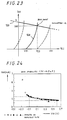
The above equation (3) is expressed by a straight
line 129 in FIG. 23, and the above-mentioned equation (7) is
expressed by a curve 128 in FIG. 23. Incidentally, the curve
128 is fluctuated as shown by a broken curve when the
threshold voltage Vth is fluctuated. Then, since the total
sum Idd of the drain currents thus obtained in actual practice
becomes a value at the intersecting point of the straight line
129 and the curve 128, an absolute value of a straight line
inclination -a must be reduced as much as possible in order to
reduce the fluctuation of the drain currents due to the
fluctuation of the threshold voltage Vth of the FET 122.
If the emitter ground current amplification factor
hfe of the transistor Q120 is selected to be several 100s of
ohms, the resistance values R121 and R122 are selected to b
several kilo ohms and the resistance value R123 is selected to
be several 100s of ohms, then the second term of the numerator
of the equation (4) is sufficiently small as compared with the
first term and therefore can be neglected. Thus, a expressed
by the equation (4) can be approximated by the following
equation (8):
a ≒ I/R124
Accordingly, if a value of several kilo ohms is
selected as the resistance value R124, then a becomes the
order of 10-4. Therefore, even if the threshold voltage Vth is
fluctuated by about 1V, then the total sum Idd of the drain
currents can be suppressed to be a small value of about zero
point and several milliamperes.
FIG. 24 shows examples of measured values of total
sum Idd of other lot of the MMIC. Study of FIG. 24 reveals
that the total sum Idd of the drain currents falls within a
range of 4mA ± 6% over a range in which the threshold voltage
Vth falls in a range of -0.1 to 0.6V, thereby obtaining a
satisfactory stability.
Since the bias stabilizing circuit according to this
embodiment is operated by the single
positive power supply, there is some different restriction
shown by the equation (6). Since the voltage that is applied
to the gate of the FET 122 in actual practice becomes such one
that results from superimposing the input signal voltage from
the input terminal Tin on the gate bias voltage Vgg, the gate
bias voltage Vgg must be set to a value that is lower than the
diffusion potential Vbi by at least about zero point and
several Volts. In this case, if it is considered that a
fluctuation relative to the threshold voltage Vth of B in the
equation (7) is small, then the application range of the gate
bias voltage Vgg can be directly replaced with the tolerance
fluctuation range of the threshold voltage Vth.
Accordingly, in the case of the GaAs MES-FET or HEMT
(high speed electron mobility transistor) in which the
diffusion potential Vbi is about 0.6 to 0.7V by using the
Schottky junction, it is considered that the tolerance range
of the threshold voltage Vth (gate bias voltage Vgg) is about
0.3V at most. Accordingly, it is to be appreciated that the
stability of the total sum Idd of the drain currents has not a
so large predominance as compared with bias stabilizing
circuits of other types. However, in the case of J-FET, the
diffusion potential Vbi is about 1.2V so that a difference of
the diffusion potential Vbi leads to the enlargement of the
tolerance range of the threshold voltage Vth as it is.
Therefore, the value thereof becomes about 0.8V and it is to
be appreciated that the J-FET has a high predominance.
The bias circuit according to the eighth embodiment
can be wholly or partly formed within
the monolithic IC as a part of the MMIC including the bipolar
transistor Q100 and the capacitors.
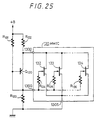
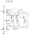
FIGS. 25 and 26 show tenth and eleventh embodiments,
respectively. In the tenth
embodiment shown in FIG. 25, a base of a transistor Q130 is
directly coupled to the collector thereof. In the eleventh
embodiment shown in FIG. 26, FETs 142, 143 and 144 within the
MMIC are each formed of P-channel type FETs and a transistor
Q140 is formed of an NPN-type transistor. Circuit
arrangements and operations of the tenth and eleventh
embodiments will not be described below.
While the FETs in the MMIC is formed of GaAs FETs as
described above, the present invention is not limited thereto
and may be formed of other compound semiconductor FETs.
Further, the FETs within the MMIC according to the present
invention is not limited to the J-FET and may be formed of
MES-FETs, HEMTs or the like. Furthermore, the FET of the MMIC
according to the present invention is not limited to the
enhancement type FET and may be formed of a depletion type
FET.
As described above,
there are provided the bias stabilizing circuit in
which one output electrode of the bipolar transistor in which
the bias voltage is applied to the base thereof is connected
to the power supply through the first resistor and the other
output electrode thereof is grounded through the second
resistor and the FET that is formed of the compound
semiconductor and which is biased by the above bias
stabilizing circuit. Further, one output electrode of the
bipolar transistor is connected to the one output electrode of
the FET and the other output electrode of the bipolar
transistor is connected to the gate of the FET. Therefore,
the bias stability is high and the tolerance fluctuation width
of the threshold voltage is wide, which is therefore
advantageous from a manufacturing technology standpoint.
Therefore, it is possible to obtain the bias stabilizing
circuit for a field effect transistor formed of a compound
semiconductor which can be driven by the single low voltage
power supply.
Furthermore, when the FET is formed of the J-FET,
the tolerance fluctuation width of the threshold voltage can
be widened more as compared with the FETs of other kinds.
Having described preferred embodiments of the
invention with reference to the accompanying drawings, it is
to be understood that the invention is not limited to those
precise embodiments and that various changes and modifications
could be effected therein by one skilled in the art without
departing from the scope of the invention as defined
in the appended claims.